


Introduction
Chipless radio frequency identification (C-RFID) technology is of increasing interest to both industry and academia due to its ability to track the object, monitor object health, and various environmental parameters at low cost. The use of RFID tags in tracking systems, industry, telecommunication, commerce, and health monitoring has significantly increased due to their low cost, simple circuitry, and data-sensing abilities [Reference Ali, Jafri, Habib, Amin and Tenhunen1, Reference Habib, Ali, Kiani, Ayub, Abbas and Butt2]. Additionally, sensors have been reported [Reference Dey, Saha and Karmakar3] for monitoring environmental parameter variations such as temperature, ambient humidity, pressure, gas, strain, and crack sensing.
C-RFID tags consist of a substrate, which provides mechanical strength, and a copper layer with a geometrical structure. This geometrical structure produces a spectral signature in the backscattered radar cross section (RCS), which is used for data encoding. These data can be either used as an identification (ID) number or for monitoring environmental parameter variation [Reference Dey, Saha and Karmakar3]. According to microstrip antenna theory, the dielectric substrate's effective permittivity affects the tag's spectral signature [Reference Sainati4]. Therefore, an ID-based tag should have a constant permittivity, irrespective of environmental variation. A 35 IDs caring C-RFID tag was reported in [Reference Khan, Tahir, Farooqui, Shamim and Cheema5], which was designed on a Taconic TLX-0 substrate with a constant relative permittivity. Closed-loop [Reference Khan, Tahir, Farooqui, Shamim and Cheema5], rectangular split ring [Reference Amin and Karmakar6], metal strip [Reference Amin, Bhuiyan, Karmakar and Winther-Jensen7], circular split ring [Reference Javed, Habib, Amin, Loo, Akram and Tenhunen8], spiral resonators [Reference Amin and Karmakar9], and circular loop [Reference Vena, Perret and Tedjini10] are commonly reported resonators used in chipless RFID tags for encoding data IDs.
To incorporate environmental parameter variations, the chipless RFID tag is covered or designed on such substrates whose relative permittivity is sensitive toward the change in the monitoring parameter [Reference Dey, Saha and Karmakar3]. This impact on relative permittivity causes a corresponding drift in the slot spectral signature. Thus, a particular parameter variation is recorded. A humidity monitoring C-RFID tag is designed on a paper substrate, whose relative permittivity changes with humidity-level variation [Reference Feng, Xie, Chen and Zheng11].
C-RFID tags were reported in [Reference Ali, Jafri, Habib, Amin and Tenhunen1, Reference Dey, Saha and Karmakar3, Reference Amin, Saha and Karmakar12–Reference Guerchouche, Herth, Calvet, Roland and Loyez15] for both ID encoding and sensing the environmental humidity variation. In these tags, the ID's slots were designed on stable dielectric substrates, while the sensing slot was coated with the polymers whose relative permittivity is sensitive toward environmental humidity variation. This leads to a constant spectral signature for ID encoding and a drifting spectral signature for the sensor slot. A humidity and temperature sensor was reported in [Reference Amin, Karmakar and Jensen16] by using phenanthrene and polyvinyl alcohol (PVA) with dielectric-sensitive nature. A temperature and carbon sensor is also designed using the substrate's dielectric sensitivity phenomena [Reference Vena, Sydänheimo, Tentzeris and Ukkonen13]. In summary, all above reported sensors are based on the impact of dielectric permittivity-sensitive nature toward a particular environmental variation. In order to harness the benefits of tags, it is essential to understand the effect of a substrate's dielectric properties on which the tags are designed. The substrate's dielectric properties are used for properly designing and simulating the tag's RCS.
This research evaluates the designing of a five-slot hexagonal shape tag in 30 × 35 mm2 area. Then a detailed simulation was performed to observe the impact of a range of different dielectric substrates on a generalized five concentric hexagonal shape tag at room temperature. The resonant spectral signatures occupied bandwidth and RQF was analyzed. The later section covers how to adjust the spectral signature in a specific bandwidth by fine-tuning of design variables such as substrate height, tag size and slot size. At the end, the proposed tag was manufactured on FR4, Roger Duroid 5880, and polyethylene naphthalate (PEN) substrates. This work is mostly focusing on the impact of different substrates having similar tag geometry, which further leads to design a novel substrate by pouring nanomaterials at a specific bar coating thickness. Before introducing the novel substrate, it is critical to observe the impact of dielectric substrate on a generalized tag's geometry. The ongoing work is focusing on a laser printed tag on these novel substrates. Some of the nanomaterials are highly sensitive toward environmental parameter variation such as humidity, temperature, CO2, and methane gas, and will be used as sensors.
Tag designing
The main objective of this article is to design a C-RFID tag whose spectral signature can be achieved with a range of different dielectric substrates as per the application requirement to improve the practical implementation. The hexagonal shape slots were selected for geometrical structure due to its space-efficient, maximum angular stability, and minimum mutual coupling [Reference Ali, Mackenzie, Lester, Williams and Greedy17, Reference Ali, Smartt, Lester, Williams and Greedy18]. CST designing and simulating software was used for designing the basic unit. A FR4 substrate with 1.6 mm height, 4.3 dielectric constant, 0.025 tangent loss, and 35 μm thick copper cladding was used for designing and producing the base unit. The tag has no ground plane, which makes it more attractive from manufacturing point of view. Equation (1) was used for calculating the radius “Rs” of hexagonal shape slot for a particular frequency “fres”. Here “C” is the speed of light and “ɛr” is the relative permittivity of the substrate used.
Equation (1) was used for calculating resonance frequencies (or slot size) for circular shape slots reported in [Reference Noor, Habib, Amin, Loo and Tenhunen19]. The obtained values from equation (1) are not in accordance with simulated and measured values of hexagonal shape tag [Reference Habib, Ali, Kiani, Ayub, Abbas and Butt2]. Probably this equation is designed only for “U-shape” tag. Therefore, the empirical equation is modified according to simulated and measured results of the hexagonal shape tag, as shown in equation (1A). The modification process increases the numerator from “2” to “3.5”, so that the empirical values could match with the simulated values. The simulated and calculated values from empirical equation (1A) are listed in Table 1. The wider slot could be easily manufactured; however, it will increase tag size and produce a spectral signature with wider span [Reference Ramos, Ali, Vena, Garbati and Perret20]. Therefore, 0.5 mm slot width is a good trade-off between tag's manufacturing and producing a reasonably narrow spectral signature, shown in Fig. 1. The plane waves were incident for exciting the tag, which is reflected back in the form of spectral signatures at a particular frequency. The RCS probe was placed 70 cm away in z + direction. Its RCS response of 33 dBsm magnitude dip was achieved after illuminating the tag with a plane wave, shown in Fig. 1, where the RCS was expressed in decibels per square meter (dBsm). Thus, it can be used as a 1-bit data encoding chipless tag. For further increasing data capacity, the same designing approach was followed by adding two and three hexagons and extended to two- and three-slot tags with 0.5 mm slot widths and gaps respectively. A disturbance can be seen in the RCS at lower frequency with addition of slots; however, the RCS signature was kept to a minimum of 5 dBsm magnitude so it could not be masked by this disturbance [Reference Ali, Smartt, Lester, Williams and Greedy18]. Additionally, in future work the disturbance reason at lower frequency will be investigated (Fig. 2).


A single hexagonal slot of radius 10 mm and its RCS response having a spectral signature at 4.272 GHz.

One-, two-, and three-slot tags with 0.2 mm slot width and gap, respectively, along with their corresponding RCS response.

Each slot radius, width, gap, guard band between them, and calculated/simulated resonating frequency are given

The units used are mm and GHz.
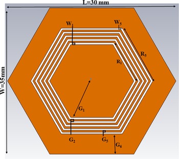
The same approach and stepwise optimization were followed to achieve a five-bit tag in a compact size of 30 mm× 35 mm, shown in Fig. 3. During the design, it has been observed that the addition of additional slot has an impact on the earlier slot's spectral signatures in terms of resonating frequencies, magnitude dips, and guard band. Therefore, a minimum spacing of 0.5 mm was used to avoid and minimize the coupling effect. Seventeen hexagonal slots were accommodated in a small patch of 5 cm2. Here we used only five slots to observe the impact of different dielectric substrate. The reason of selecting hexagonal shape slot instead of other structure (geometry) is higher code density, and higher angular readability, reported in the preceding work [Reference Ali, Smartt, Lester, Williams and Greedy18]. The detailed comparison of 18-slot tag with recent literature is also elaborated in the preceding work [Reference Ali, Smartt, Lester, Williams and Greedy18].
The slot radius is denoted by “Rx”, width by “Wx”, and gap by “Gx”. “L” and “W” are the length and width of the tag, respectively. The detailed values are given in Table 1.

The design variables in the proposed tag are the total tag size, radius, widths, gaps between slots and substrate height, and types. This leads to 10 geometric parameters that need to be optimized, which could also control the coupling effect. Figure 3 shows the design variables that effect the RCS spectral signatures, which consist of slot radius (R 1, R 2, … R 5), gaps between them (G 1, G 2, … G 6), and tag size (L × W). The calculated and optimized values of all these parameters are given in Table 1. Furthermore, the substrate thickness and change in relative permittivity also affect the RCS spectral signatures. The detailed analysis is described in the following sections.
Results and discussion
The simulated results were achieved by placing an RCS probe in the far field and capturing simulated RCS response of the tag. The tag was placed 70 cm distance (d) away from the probe in the z + direction. The distance “d” was calculated using equation (2), where “D” is the maximum dimension of tag and “λ” is the central wavelength (0.0952 m) of the used central operating frequency (3.15 GHz) [Reference Habib, Ali, Kiani, Ayub, Abbas and Butt2]. In our proposed tag each side of the tag is 1.5 cm (a = 15 mm); below calculation was used to find the maximum dimension (D) of the hexagonal shape tag [21], and distance (d) between probe and tag.


The backscattered signatures were captured with the RCS probe, as shown in Fig. 4. The captured RCS data have distinguished spectral signatures for the corresponding 5-bit tag, which means the number of slots has 1:1 correspondence to the number of encoded spectral signatures. This tag can be extended to an n-number of slots by adding more slots and increasing the total size which gives 2n different IDs [Reference Ali, Mackenzie, Lester, Williams and Greedy17].
RCS response of 5-bit tag with FR4 substrate, bit (B 1) corresponds to the resonator (R 1) and vice versa.

The reported findings in the field of C-RFID suggest that larger slot produces a spectral signature at a lower frequency. On the contrary, if the tag size is very small, it leads to smaller resonating element and produces resonating notches at a higher frequency. These small size tags also led to a lower reading range and some of them were only detected in the near-field region (up to few centimeters) [Reference Herrojo, Mata-Contreras, Paredes, Núñez, Ramon and Martín22]. These resonating notches/spectral signatures were also strongly dependent on the substrate or covering material's relative permittivity [Reference Ali, Jafri, Habib, Amin and Tenhunen1, Reference Dey, Saha and Karmakar3, Reference Amin, Saha and Karmakar12–Reference Nair, Perret, Tedjini and Baron14, Reference Amin, Karmakar and Jensen16]. This dependency can be further explained with equations (1A) and (3) [Reference Sohrab23], where the spectral signatures are strongly dependent on relative permittivity of a dielectric substrate as well as perimeter of the slot radius. In equation (3) “ɛeff” is the effective permittivity of the substrate or covering material, “ɛr” is the relative permittivity, h is the used substrate thickness, and w is the width of the patch along XY plane.

Equations (1A) and (3) suggest that the resonant frequency of a slot depends on its radius and the effective permittivity of the dielectric substrate. It also describes if the slot radius, substrate thickness, and patch width are kept to a constant value, then the spectral signature is dependent only on the substrate or covering material's effective permittivity. To validate this statement, a fix copper layer geometry was replicated over various dielectric materials and its impact was analyzed on the tag's spectral signature.
Tag response for various dielectric substrates
The dielectric substrate has an impact on the tag's spectral signatures due to effective permittivity, radiation loss, conduction loss, and dielectric loss [Reference Vena, Perret and Tedjini24]. Radiation loss is useful in our case, while conduction and dielectric losses should be as small as possible. Conduction loss can be controlled by using a thick copper layer, but careful attention is needed while choosing an appropriate substrate.
To analyze the substrate impact, the proposed tag's copper geometry was replicated over a range of dielectric substrates [Reference Ahmad and Silaghi25]. In CST, some of these material models are ideal, i.e. their tangent loss is zero, while others are lossy. In this analysis, lossy material models were used to obtain simulations near to real-time measurement.
The evaluation was performed using the time-domain method in the commercially available Electromagnetic Simulation Technology (CST) studio suite software provided by 3DS Simulia [26]. Three methodologies were used for the evaluation. In the first method, the copper geometry and dimension of the tag were kept fixed for all substrates. Then the impact on the spectral signature's occupied bandwidth, minimum resonance quality factor (Min RQF), and maximum resonance quality factor (Max RQF) was recorded from CST simulation. In the second evaluation, the tag design variables such as copper geometry, slot size, tag dimension, and substrate thickness were optimized to adjust the spectral signature's occupied bandwidth and Min/Max signature depth. In the third step, the proposed tag geometry was manufactured on Fr4, Roger Duroid 5880, and PEN substrates for experimental analysis of dielectric substrate's impact.
Simulation setup I
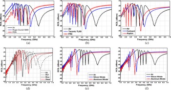
A range of dielectric substrates such as air, PEN, Roger Duroid 5880, Taconic TLX-0, polyethylene terephthalate (PET), cardboard, Kapton, FR4, glass, mica, silicon nitrate, aluminum nitrate, alumina, silicon, and gallium arsenide were used for a fixed tag's geometry, shown in Fig. 5. The electrical properties and simulated results of the first evaluation setup were recorded in Table 2 and Fig. 5. It was ensured that during simulations the spectral signatures should be at least 5 dBsm in magnitude and above the −90 dBsm level, so the spectral signatures could be detectable in real-time measurement. The tag with the air substrate was used as a reference for comparison, which occupied a 2.17 GHz bandwidth with a 14 dBsm minimum depth signature, shown in Fig. 5(a). The copper geometry was then replicated over PEN and Roger Duroid 5880 substrates, the simulated results show a 0.337 and 0.37 GHz bandwidth compression, respectively, as shown in Fig. 5(a). However, the spectral signature was quite clear and minimum signature depths are 14 and 6 dBsm, respectively. Figures 5(b)–5(d) show the relevant band compression and variation in signature depths for Taconic TLX-0, PET, cardboard, Kapton, FR4, and mica. All these dielectric substrates had an impact on the tag's resonance frequencies, minimum and maximum signature depths, and resonance quality factor (RQF). However, spectral signatures still have a 5 dBsm min depth which could be easily detectable in real-time measurements. Moreover, the resonant frequencies obtained from equation (1A) and the simulations were similar.
Impact of different dielectric substrates having different effective permittivities over a generalized five hexagonal slot tag RCS response. The air was set as reference and compared with (a) PEN and Roger Duroid 5880, (b) Taconic TLX-0 and FR4, (c) cardboard and Kapton, (d) PET, mica, and glass, (e) silicon nitrate and aluminum nitrate, and (f) alumina, silicon, and gallium arsenide.

Electrical properties of a range of dielectric substrates and its impact on tag's occupied bandwidth and resonance quality factor (RQF)

As shown in Table 2, the permittivity “ɛr” increased for silicon nitrate, aluminum nitrate, alumina, silicon, and gallium arsenide due to which the spectral signature shifted toward lower frequencies and some of them disappeared as shown in Figs 5(e) and 5(f). The poor backscattered radiation suggests that the tag structure as is does not resonate for these substrates. Altering the width, length, thickness, or slot size of the tag could improve the backscattering radiations.
Resonance quality factor
RQF plays a major role in analyzing the impact of different dielectric substrate on tag's spectral resonances. RQF defines the magnitude and compactness of a spectral signature's resonance [Reference Sajitha and Mohanan27, Reference Khanna and Garault28], these both parameters are desirable in the tag's RCS response. High magnitude RCS signature is very less effected from floor noise, therefore literature suggests that the RCS signatures should not be smaller than 5 dBsm in magnitude [Reference Ali, Jafri, Habib, Amin and Tenhunen1]. While the compactness property of RCS signature could maximize the number of encoded bits per frequency spectrum. Additionally, high RQF also leads to higher read range. The RQF could be calculated by using equation (4) [Reference Khanna and Garault28], where “fc” is the resonance central frequency, “f 1” is lower frequency than “f c” when the power of resonance is raised to 3 dB as compared to “fc” power, similarly, “f 2” is a higher frequency than “f c” when the power of resonance is raised to 3 dB as compared to “f c” power. FR4-based tag's RQF is calculated for all slots, shown in Fig. 6. Figure 6 shows that slot 4 has the highest RQF (70.04) due to its compactness and high magnitude resonance. In contrary, slot 5 has the lowest RQF (9.28) due to the wide span resonance. In the next section, the impact of different dielectric substrate will be analyzed based on the RQF values for all signatures. The average RQF (A-RQF) could be used for comparison of tag's spectral signature depth and span, such as air-based tag has 49.33 A-RQF. Before optimization glass gives highest A-RQF = 65.24, however after tags structure optimization for high dielectric substrate silicon nitrate gives the highest A-RQF = 51.33, shown in Table 2.

Slot 5 signature's 3 dB power, f 1, f 2, and f c are shown, while each resonance RQF is calculated from their corresponding values of f 1, f 2, and f c.

Simulation setup II
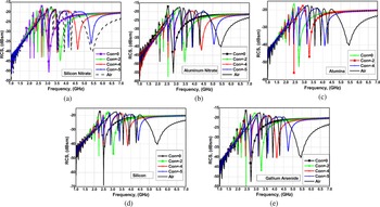
The recorded data in Table 2 and Fig. 5 show that the substrate's electrical properties had an impact on the tag's performance in terms of signatures depth, RQF, and occupied bandwidth. The evaluation was performed at the resonant frequencies occurring per configuration. The simulated data show that thick substrates of high permittivity “ɛr” lead to poor radiation, spectral signature compression, and shifting toward lower frequency band. Substrates with high permittivity “ɛr” such as silicon nitrate, aluminum nitrate, alumina, silicon, and gallium arsenide result in low radiation. Therefore, in the second simulation setup the tag design variables were adjusted for lossy substrates so that the spectral signature could become detectable. Several iterative simulations were performed on design variables such as substrate height, tag size, and slot size. These iterative simulations were performed for silicon nitrate, aluminum nitrate, alumina, silicon, and gallium arsenide substrates and compared with the tag having the air substrate. During these iterative simulations, it was necessary to achieve the Min 5 dBsm size signature to encode as data, otherwise the signal to noise ratio of the spectral signature is small and at risk to demolish with noise. In these iterative simulations, the slot size was found to be a key variable, which affects the spectral signature's occupied bandwidth and Min/Max signatures depth. The increase in slot size further reduced the signature depth. However, the iterative decrease in slot size improved the signature depth, as shown in Fig. 7. The simulated data in Fig. 7 show that tags made of lossy substrates could also resonate and give a clear spectral signature at the cost of reducing slot size. This reducing slot size also leads to a smaller size tag.
The tags having high dielectric permittivity “ɛr” substrate, their all-slot size was contracted “Con” to achieve a clear spectral signature such as (a) silicon nitrate Con = −5, (b) aluminum nitrate Con = −5, (c) alumina Con = −4, (d) silicon Con = −5, and (e) gallium arsenide Con = −5.

In Fig. 7, “Con” is the iterative contraction in slot size as compared to original slot sizes given in Fig. 3. The iterative contraction “Con” is different for different substrates, starting from Con = 0 and contracting to Con = −5 mm. The tags having substrates of silicon nitrate, aluminum nitrate, and silicon gave clear spectral signatures when all slots were contracted by Con = −5 mm. However, in the case of alumina, a clear spectral signature could be achieved by contracting all slots up to Con = −4 mm as shown in Fig. 7(c). The current work state-of-the-art comparison is given in Table 3. This work improved in achieving high A-RQF, smaller occupied bandwidth, multiple printing technique, and tag geometry replicability on 15 different substrates.
Comparison of current work with reported literature

These analyses will play a key role for picking up the right dielectric substrate at the time of designing a chipless RFID tag for an application. Some of the applications need a normal size chipless RFID tag with no sensing functionality, such as that used in shopping mall for tagging the items [Reference Amin, Saha and Karmakar12]. In such applications, thin substrates with low tangent loss and low permittivity, such as PEN, Roger Duroid, Taconic TLX-0, PET, cardboard, Kapton, FR4, and mica, are used for designing RFID tags [Reference Khan, Tahir, Farooqui, Shamim and Cheema5, Reference Amin, Bhuiyan, Karmakar and Winther-Jensen7, Reference Ali, Mackenzie, Lester, Williams and Greedy17, Reference Vena, Perret, Tedjini, GEP, Delattre, Garet and Boutant30–Reference Dey and Karmakar32]. In contrast, other application needs a smaller size tag such as 5G technology [Reference Hasan, Noordin, Karim, Rejab and Ma33], along with environmental parameter monitoring/sensing functionality. To incorporate environmental parameter variation, the dielectric substrate's electrical properties (such as dielectric permittivity and dielectric loss) sensitivity toward environmental variations; for example Kapton relative permittivity is effected by change in humidity level [Reference Ali, Jafri, Habib, Amin and Tenhunen1]. This effect had an impact on tag's spectral signatures in terms of RQF or resonating frequency. Using this spectral signature sensitivity toward variation in relative permittivity “ɛr” produces a range of C-RFID sensor tags, and more are expected to be designed in near future for sensing various environmental parameter variations such as humidity, temperature, methane, oxygen, and CO2 sensors [Reference Ali, Jafri, Habib, Amin and Tenhunen1, Reference Dey, Saha and Karmakar3, Reference Amin, Bhuiyan, Karmakar and Winther-Jensen7, Reference Feng, Xie, Chen and Zheng11, Reference Amin, Saha and Karmakar12, Reference Nair, Perret, Tedjini and Baron14, Reference Barahona, Betancourt and Ellinger34].
Additionally, this analysis also provides a pathway for designing an RFID tag on other dielectric substrates which are developed but not used in RFID tags or not developed yet. Hypothetically, the substrate's large losses could be controlled by doping with different dielectric materials at the molecular level [Reference Baklanov and Maex35]. Thus, a substrate with high dielectric constant and losses could be reduced by adding a lower dielectric constant material in a regular pattern [Reference Psychoudakis, Koh, Volakis and Halloran36], and vice versa. Based on this hypothesis, a novel substrate was produced which is elaborated in section ‘Producing a novel substrate from nanomaterials’. Furthermore, from these analyses, it is expected that in future an application-oriented chipless RFID tag could be designed on any material or substance, such as on animal tissues, plants, organic, and non-organic substances.
Measurement setup
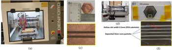
Tag manufactured by Denford milling machine
The tag was manufactured on Fr4, Roger Duroid 5880, and PEN substrates to validate the different substrate's impact on the tag's spectral signature in a real-time scenario. The Denford milling machine and FujiFilm Dimatix inkjet printer were used for tag manufacturing at the University of Nottingham. Since the available milling bit has a 0.5 mm diameter, the minimum slot width and gaps were being kept to 0.5 mm. The tag has the same geometrical parameter as described in Table 1 and Fig. 1. The simulated tag geometry was written in Computer Numerical Control (CNC) Programming and loaded to Denford milling machine [37]. The used PCB had 35 μm thick copper cladding, which is received from RS. The milling machine engraved the copper from a single-sided PCB according to the loaded code. The manufacturing process and produced hexagonal shape tags are shown in Figs 8(b) and 8(c). Using the proposed manufacturing process, tags with different slot configuration were designed such as five slots, three slots, two slots, and a plate sheet.
(a) The proposed tag manufacturing process using Denford milling machine and manufactured hexagonal shape tag with, (b) two slots on FR4 substrate, (d) silver tag manufacturing process by Dimatix Materials Printer, (e) silver printed tag on PEN substrate, (f) zoomed view of the silver tag.

Tag manufactured by inkjet printer
An inkjet printed tag with silver nanoparticles was reported in [Reference Ramos, Ali, Vena, Garbati and Perret20]. In this work a tag with five slots was manufactured using a Dimatix Materials Printer (DMP-2850, Fujifilm) and a 10 pL drop volume cartridge (DMC-11610), shown in Fig. 8(d). The silver nanoparticle (AgNP)-based conductive ink (SilverJet DGP-40LT-15C, Advanced Nano Products, Sejong, South Korea) was deposited on a PEN substrate (75 μm, GTS Flexible Materials LTD). A drop spacing distance of 30 μm and a substrate temperature of 90°C were used to achieve continuous and uniform surface morphology of the printed layer. The printed Ag tag (three layers) on the PEN substrate was then sintered in an oven at 150°C for 1 h for high conductivity, shown in Figs 8(e) and 8(f). The electrical resistivity of a single printed Ag layer was measured to be ~13 μΩ.cm [Reference GF, F, Im, He, Balogh, Scurr, Gilmore, M, E and Pervan38]. This tag (PEN-based substrate) is fully flexible as compared to Fr4 and Roger-based tag.
Manufactured tag measurement
To measure the backscattered S21 response of manufactured tags, a bi-static antenna setup was used, shown in Fig. 9. The setup consists of vector network analyzer (VNA) where both ports of VNA were connected to two double-ridged horn antennas having 0.7–18 GHz bandwidth and 12 dBi gain. One antenna was used as a transmitter (Tx) and the other was used as a receiver (Rx) for capturing the backscattered S21 from the tag. Different measures were considered for achieving good accuracy. First the antenna and tag calibration setup were set inside anechoic chamber. Second, the Tx and Rx antenna were separated by a distance of 120 cm along with installing an absorber to minimize the cross-coupling between two port signals and with environmental electromagnetic signal, as shown in Fig. 9. The manufactured tag was placed 70 cm away from two antennas. However, strong coupling still existed between antennas. Therefore, a calibration technique was used to remove these unwanted static effects. The calibration was performed by capturing three different complex S21 parameters. First, an initial calibration technique was used to remove these unwanted static effects. The calibration was performed by capturing three different complex S21 parameters. First, an initial measurement of empty anechoic chamber without tag was done and referred as NoTagS21. Then, the second measurement was performed with equal size square plate target, which is referred as a RefTagS21. The reference target, RefTagS21, RCS was calculated by CST simulation and referred in equation (5) as SimRCSPlate. Finally, the desired tag was placed in front of antennas and captured their reflections and referred as TagS21. The captured reflected data were processed in Matlab according to equation (5) [Reference Ali, Smartt, Lester, Williams and Greedy18].

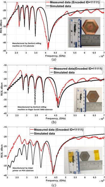
Five-slot tag printed with milling machine on (a) FR4 substrate, (b) Roger Duroid 5880 substrate, and (c) printed with FujiFilm Dimatix printer on PEN substrate (flexible tag).

Impact of substrate on tag's spectral signature
To validate the simulated data of section ‘Tag response for various dielectric substrates’, the copper geometry of Fig. 3 was manufactured on three different substrates FR4, Roger Duroid 5880, and PEN, shown in Figs 9(a)–9(c). The tags manufactured on FR4 and Roger Duroid 5880 were nonflexible, while PEN-based tag is flexible. All tags had the same geometry, which is 0.5 mm slot width and gapes between slots, except having different substrates. To observe and analyze the substrate impact on the tag's spectral signature, the designed tag's backscattered S21 response was measured using the same setup as elaborated in [Reference Habib, Ali, Kiani, Ayub, Abbas and Butt2]. The backscattered S21 response presents the impact of different substrates in terms of shifts in spectral signatures. Although, the tag has been manufactured by different mechanisms such as milling machine and inkjet printing. However, the different manufacturing has very less impact as compared to the impact of different substrates [Reference Brinker and Zoughi39]. Additionally, the simulated and measured backscattered S21 response has a strong agreement. Figure 9(c) presents that the spectral signature's QF is reduced presumably due to very thin layer (1.2 μm) of deposited silver nanoparticles. In the ongoing research, the conducting layer thickness and spectral signature's QF relation will be investigated. The detailed simulated and experimental data reveal the impact of various substrates on the tag's spectral signatures.
Producing a novel substrate from nanomaterials
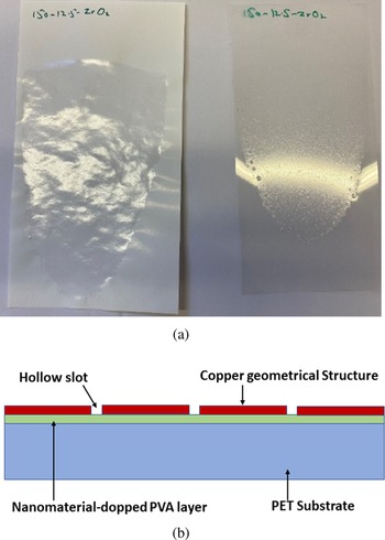
The above analysis of substrate impact on tag's spectral signature leads us to designing an application-oriented substrate, where a novel substrate was designed from nanomaterials to harness the better sensing functionality of chipless RFID tags. The method used for this new substrate designing was pouring the nanomaterials on PET and photo printing paper with specific thickness. The K-bar was used for achieving 12–500 μ thick layers of nanomaterials. The nanomaterials used are PVA, TiO2, ZnO2, ZrO2, and CeO2. PVA itself is hygroscopic and absorbs water, which can be poured on top of chipless RFID tag and can be used as a humidity sensor [Reference Dey, Saha and Karmakar3, Reference Amin, Saha and Karmakar12]. However, from these tags the PVA can be easily peeled off or go away with chemical reactions. In our proposed work the above-mentioned nanomaterials were doped with PVA with different ratios starting from 5 g PVA:50 g water:10 g nanomaterial. Then, the nanomaterials will be sandwiched between PET/paper and tag's copper structure, as show in Fig. 10. The reason of producing such a tag is accurate sensitivity toward variation in environmental parameter such as humidity, temperature, CO2, and other gases [Reference Beaulieu, Baral, Hendricks, Tang, Briseño and Watkins40]. To design such a versatile and application-oriented substrate, a 12.5 g PVA was gradually added in 50 g zirconia water solution and magnetically stirred for 2 h at 120°C. This PVA-doped zirconia-water-solution was allowed to cool down to room temperature. Then a 3 ml PVA-doped zirconia-water-solution was poured on paper and PET substrate using transparent plastic pipette. The poured nanomaterial was distributed at 150 μ thickness, in the form of film, using a handheld k-bar. The prepared modified substrate was dried for 24 h at a room temperature, shown in Fig. 10. In the ongoing research work, an inkjet printed tag will be manufactured on this novel substrate instead of PEN substrate, as shown in Fig. 9(c), and will be tested for various temperatures, as a temperature sensor.
(a) A 150 μ thick PVA-doped-zirconia layer on paper and PET substrate. (b) Nanomaterial sandwiched between substrate and copper geometrical structure.

This research provides a real-time tag which has the following advantages over to-date reported work:
• The tag geometry could be realized on a range of dielectric substrates, which makes the tag more convenient for the realization.
• Different tag's printing processes were used to print the tag on three different substrates and found that each one simulated and measured RCS resonating nulls at similar frequencies, however the magnitudes are not similar.
• The analysis of different dielectric substrate provides a pathway of designing a novel substrate by using nanomaterials for better environmental-sensing functionality.
Conclusion
The impact of a range of dielectric substrates was analyzed over a generalized five-slot hexagonal shape tag. The simulated data show that the best spectral signatures were achieved with air having dielectric permittivity of ɛr = 1. The analysis shows that the degradation occurs in RQF and occupied band width increases with ɛr. This degradation could be controlled by adjusting the design variables. The slot size was found as the key design variable to control the QF and occupied band degradation. The tag was manufactured on FR4, Roger Duroid 5880, and PEN substrates by using Denford milling Machine and inkjet printing. Bistatic antenna setup was used to capture the tag's backscattered S21 response. The impact of different dielectric substrates on tag's backscattered S21 responses was analyzed by using CST simulations and experimental data comparison. The resonating nulls of simulated RCS response were in good agreement with the measured data, however some signature magnitudes are not similar.
The analysis of different substrate effects leads us to design a novel substrate using dielectric nanomaterials. In future, the tag will be printed on the produced substrate by using inkjet printing process. The dielectric properties of this novel substrate hypothesized that the produced tag with novel substrate will be having better monitoring capability of environmental parameter variations.
The ongoing current work is focusing on tag's geometry printing on novel substrate by using different printing techniques such as laser printing, and silver nanoparticle depositions. The outcome of ongoing research will be a versatile temperature sensor tag.
Acknowledgements
The work was supported through the provision of a cooperation license for the CST Studio Suite within 3DS Simulia by Dassault Systems, and the government of Pakistan for providing support and funding in this research.
Conflict of interest
None.
 Amjad Ali is currently pursuing his Ph.D. degree in Electrical and Electronics Engineering from the Department of Electrical Engineering in the University of Nottingham, UK. His research interest is designing chipless RFID tags for tracking biomass pellets supply chain and monitoring their ambient humidity, temperature, and CO2 level. He also joined GGIEMR Research Group in 2018 at the University of Nottingham, UK.
 Dr. Christopher Smartt received the M.Eng. and Ph.D. degrees in Electrical and Electronic Engineering from the University of Nottingham in 1991 and 1995, respectively. Following 2 years working as a Research Assistant at the University of Nottingham on simulation of microwave devices, he joined BAE SYSTEMS where he worked on 2D and 3D full-field time- and frequency-domain finite-element techniques for electromagnetic field simulation in aerospace applications. In 2007, he re-joined the George Green Institute for Electromagnetics Research at the University of Nottingham as a Research Fellow where his research interests include the development and application of computational electromagnetics methods and the development of electromagnetic field measurement techniques including time-domain and near-field methods, with applications to EMC and EMI studies.
 Dr. Jisun Im is a research fellow at the Centre for Additive Manufacturing at the University of Nottingham (UK). She completed her B.S. and M.S. in Polymer Science and Engineering at the Pusan National University (South Korea) and Ph.D. in Polymer Science at the University of Massachusetts Lowell (USA). She has a postdoctoral experience at the Massachusetts Institute of Technology (USA) and 5 years of industry experience at Samsung SDI. Her expertise and research interest are the design and synthesis of multifunctional materials for sensors and functional electronics application.
 Dr. Orla Williams is an Anne McLaren Research Fellow at the University of Nottingham investigating sustainable biomass-based processing techniques to produce critical raw materials for the circular economy. She graduated from the University of Bath with an M.Eng. in Mechanical Engineering and has an Engineering Doctorate (EngD) in Chemical and Environmental Engineering from the University of Nottingham. She is also a chartered engineer (CEng) with the Institution of Mechanical Engineers (IMechE) with several years of experience in the transport, construction, and power generation sectors.
 Professor Ed Lester has expertise in fuel combustion, thermal and microscopic techniques (petrography) for the characterization and identification of renewables and coal for combustion, image analysis of particulates, characterization of biomass particularly with regards to energy conversion and the power sector. Professor Lester also has expertise in nanotechnology and sustainable production of nanomaterials using hydrothermal and solvothermal techniques. He is also Technical Director of Promethean Particles.
 Ass. Prof. Steve Greedy was born in Cardiff, UK. He received the M.Eng. and Ph.D. degrees in 1998 and 2002 from the University of Nottingham. He is an Associate Professor within George Green Institute for Electromagnetics Research. His interests are in the area of experimental and computational electromagnetics with a focus on techniques used in the study of electromagnetic compatibility and signal integrity, specifically mechanisms that impact performance and coexistence of wired and wireless communication system.


 Open access