


Introduction
Gallium nitride (GaN) technology has started dominating high power applications, especially in phased-array radars, wireless communication systems, and transmitters at millimeter-wave frequencies. GaN transistors are preferable in terms of high output power thanks to the high breakdown field, high saturation velocity, and superior thermal properties of the material. AlGaN/GaN structures can be grown on SiC substrates, having low lattice mismatch and low thermal expansion mismatch, which are ideal conditions for high power applications. Owing to these properties, AlGaN/GaN HEMTs are being used in many applications, such as high power and high gain amplifiers, as well as robust low noise amplifiers and highly survivable switches. Moreover, usage of GaN processes for transceiver modules is now in demand for a highly compact single aperture for phased array antennas.
The performance of GaN HEMTs for Ka-band has been developed over the years, and many monolithic microwave integrated circuits (MMICs) are designed with AlGaN/GaN and InAlGaN/GaN HEMT structures [Reference Darwish, Boutros, Luo, Huebschman, Viveiros and Hung1–Reference Nakatani, Yamaguchi, Hangai and Shinjo12]. At 35 GHz, a saturated power density of 4 W/mm is achieved for an AlGaN/GaN device with 0.18 $\rm\mu$ m gate length in [Reference Darwish, Boutros, Luo, Huebschman, Viveiros and Hung1]. Another AlGaN/GaN device is reported in [Reference Yu, Tao and Hong2] with a 5 W/mm power density at 35 GHz. In [Reference Din, Wojtowicz and Siddiqui4], a 40 W MMIC is realized using a process with 4 W/mm output power density at 30 GHz with 28 V operating voltage. Another high power example is given in [Reference Litchfield and Dugas5], showing an output power density of 3.2 W/mm and 24% power-added efficiency (PAE) with 24 V operating voltage. The 0.1 $\rm\mu$
 m AlGaN/GaN HEMT on SiC technology is demonstrated in [Reference Chéron, Campovecchio, Quéré, Schwantuschke, Quay and Ambacher6] with 4 W output power and 27% PAE from 29 to 31 GHz, where the saturated drain current density is higher than 1600 mA/mm. GaN on Si technology with 0.1 $\rm\mu$
 m gate length is also used for a high frequency MMIC design in [Reference Leblanc, Ibeas, Gasmi, Auvray, Poulain, Lecourt, Dagher and Frijlink7], showing 5.6 W output power and 30% PAE at 32 GHz with 12 V supply voltage. Using an InAlGaN/GaN structure, a power density of 2.7 W/mm at 30 GHz is achieved in [Reference Potier, Piotrowicz, Chang, Patard, Trinh-Xuan, Gruenenpuett, Gamarra, Altuntas, Chartier, Jacquet, Lacam, Michel, Dua, Oualli and Delage8]. Another InAlGaN/GaN HEMT work with AlGaN back-barrier introduces an improved epitaxial structure for the reduced recovery time of drain current, which would be favorable, especially for low noise amplifiers in transceivers for radar applications [Reference Piotrowicz, Jacquet, Gamarra, Patard, Dua, Chartier, Michel, Oualli, Lacam, Potier, Altuntas and Delage10]. The limitations of design for large bandwidths at Ka-band frequencies are discussed in [Reference Neininger, John, Thome, Friesicke, Brückner, Quay and Zwick11] which shows a design example with 26% PAE using 15 V operating voltage and 50 W/mm drain current. A large bandwidth is obtained in [Reference Nakatani, Yamaguchi, Hangai and Shinjo12] with 15.5 W output power and 16% PAE over 15.6% bandwidth from 26.5 to 31 GHz.
NANOTAM has been developing in-house AlGaN/GaN processes for millimeter-wave applications, with 0.2 $\rm\mu$ m gate length, using the epitaxial structure grown in the same facility. The fabricated transistor with $4\times 50\, \rm\mu {\rm m}$
 periphery has a maximum available gain (MAG) of 9 dB at 35 GHz. The average output power density of the fabricated devices is 2.9 W/mm with 34.5% PAE at the same frequency. Two standalone MMICs are designed to achieve high efficiency results at Ka-band using the HEMTs fabricated with this process. A three-stage MMIC is designed and realized, which shows a gain higher than 19.3 dB, an output power of 31.9 dB, and a PAE of 26.5% at 35 GHz. Also, measurement results show that a two-stage MMIC designed for higher output power exhibits 35.9 dB output power with 26.3% PAE at 35 GHz. These high efficiency values are achieved using 20 V drain voltage with 30% duty cycle in the measurements, which is challenging considering that other works around the same frequency range operate with 10% duty cycle [Reference Yu, Tao and Hong2, Reference Ng, Takagi, Senju, Matsushita, Sakurai, Onodera, Nakanishi, Kuroda and Soejima3, Reference Chen, Nayak, Campbell and Reese9]. To compare with the other published work and to show the large-signal performance dependency on duty cycle, PA MMIC is also characterized with 10% duty cycle and continuous wave (CW) conditions at 35 GHz, showing 28.1% and 25.8% PAE, respectively. NANOTAM's 0.2 $\rm\mu$
 m gate length technology capabilities are proven with the presented MMIC designs and measurement results.
In this paper, in-house fabrication technology is detailed in section “GaN fabrication technology”. HEMT characterization is discussed in section “HEMT characterization”, while MMIC design considerations are explained in section “MMIC design considerations”. Measurement results and comparisons with other published work are given in section “Measurement results”, and the paper is concluded in section “Conclusion”.
GaN fabrication technology
NANOTAM's in-house 0.2 $\rm\mu$ m AlGaN/GaN fabrication technology is used for Ka-band applications. The active and passive devices are fabricated on the epitaxial structure grown by metal-organic chemical vapor deposition (MOCVD) method on a 3-inch SiC substrate. The epitaxial structure is optimized to achieve high performance for Ka-band transistors. AlGaN barrier layer is grown with a thickness of 22 nm and an Al concentration of 28.4% to increase 2DEG density as much as possible without any relaxation [Reference Medjdoub13]. The buffer layer is grown with Fe-doping in the structure, with prior knowledge of the effects of the buffer layer's doping properties on the buffer leakages and the trapping mechanism. The existence of deep-acceptor traps in the C-doped buffer results in a high voltage-dependent current collapse, whereas Fe-doping only causes mild current collapse thanks to the lack of these deep-acceptor traps [Reference Uttam, Towhidur and Yuewei14]. Moreover, buffer leakage current is smaller in the Fe-doped structures due to the higher energy barrier between the channel and the buffer layer [Reference Kawada, Hanawa and Horio15].
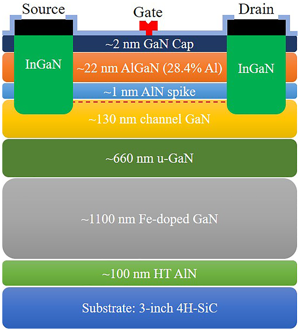
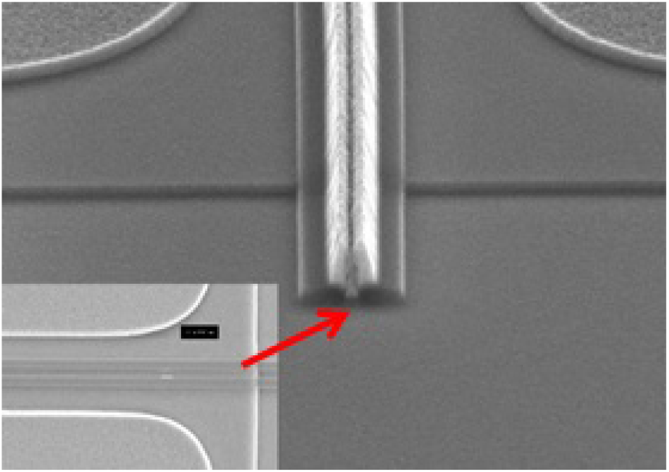
For active devices, ohmic contacts are formed as non-alloyed by growing InGaN into the AlGaN layer using the MOCVD method to define conducting sources and drains with Cr/Au metal stack. The ohmic contact resistance of the process is around 0.3 ${\rm \Omega}$ mm. The device structure showing the epitaxial layers and regrown ohmic contacts is shown in Fig. 1. The most critical step in the fabrication for higher frequencies is the gate formation, which is performed by an e-beam lithography system. A gate foot length of 200 nm with 500 nm head length is determined for this process, ensuring its uniformity and durability. After patterning the foot and head of T-gates, the foots are formed by a dose of $2000\, \rm\mu {\rm C}/{\rm cm}^{2}$
 in the e-beam lithography system. The gate formation is finalized by metallization using Ni/Au metals, followed by lift-off operation. The completed gate structure can be seen in Fig. 2. After gate metallization, a Si$_3$
 N$_4$
N$_4$ passivation layer is deposited by plasma-enhanced chemical vapor deposition. Two metal layers of Au metal are used in the process, forming the active device connections and passive structures as metal-insulator-metal (MIM) capacitors and interconnections using air-bridges in between when necessary. MIM capacitors have a capacitance density of 180 pF/mm$^{2}$
 . The fabrication also has a thin film resistor process with a sheet resistance of 30 Ω/□. To have a microstrip structure for transistors and passive elements, via holes of 85 $\rm\mu$
 m diameter are etched and filled with Au metal after thinning the wafers to 100 $\rm\mu$
 m.
m.
Device structure showing the epitaxial layers grown by MOCVD and InGaN regrowth for ohmic contacts.
SEM image of T-gate of a Ka-band HEMT, showing its 200 nm gate foot.
HEMT characterization
HEMTs, fabricated using NANOTAM's 0.2 $\rm\mu$ m GaN on SiC technology, show an average maximum drain current of 1.05 A/mm with an average transconductance of 280 mS/mm. The gate and drain leakages of such transistors are measured to be 21 μA/mm and 40 ${\rm\mu}$
 A/mm, respectively, at 20 V drain voltage. Transistors of 4, 6, and 8 fingers with 50 and 75 $\rm\mu$
 m peripheries exhibit MAGs ranging from 6 to 9 dB at 35 GHz, measured under CW operation with 20 V drain voltage and 100 mA/mm drain current. Cut-off frequency ($f_T$
 ) and maximum oscillation frequency ($f_{max}$
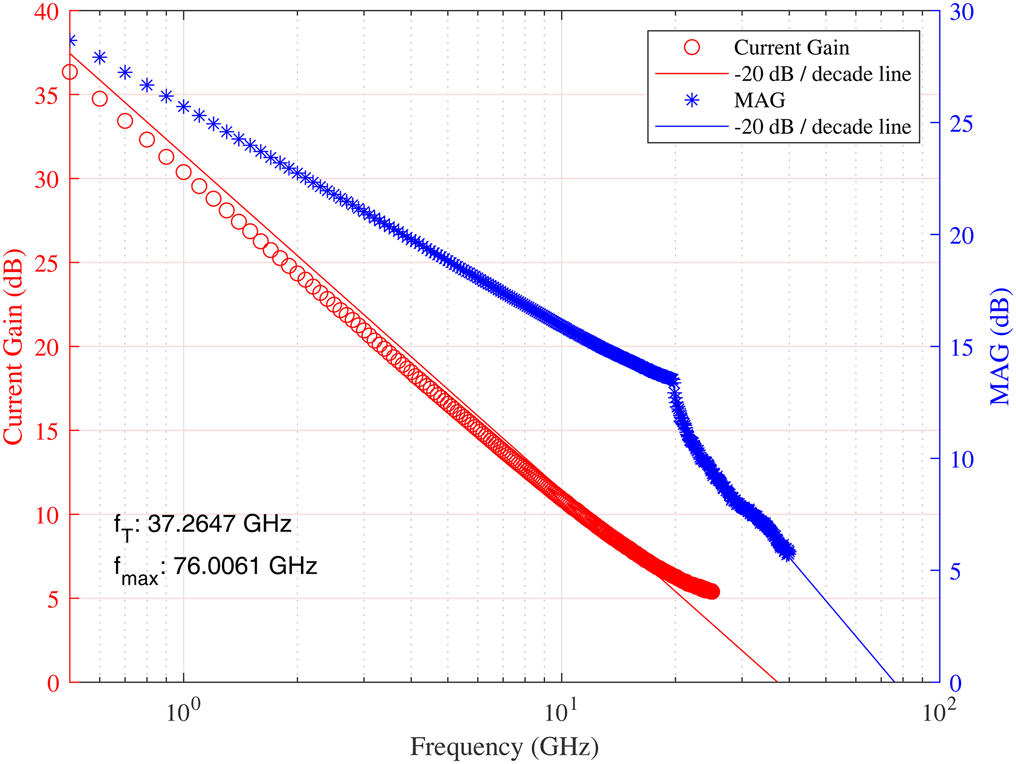
 ) of transistors are also characterized using small-signal measurement data by extrapolating the current gain and MAG curves. Figure 3 shows the results for a $6\times 75\, \rm\mu {\rm m}$
 HEMT, where $f_T$
 is calculated as 37.3 GHz and $f_{\max }$
 is calculated as 76 GHz.
Current gain and MAG graphs and extrapolated fits for $f_T$ and $f_{max}$
 calculations of a $6\times 75\, \rm\mu {\rm m}$
 HEMT.
HEMT.
Schematic of the hybrid vector-based load-pull measurement setup.
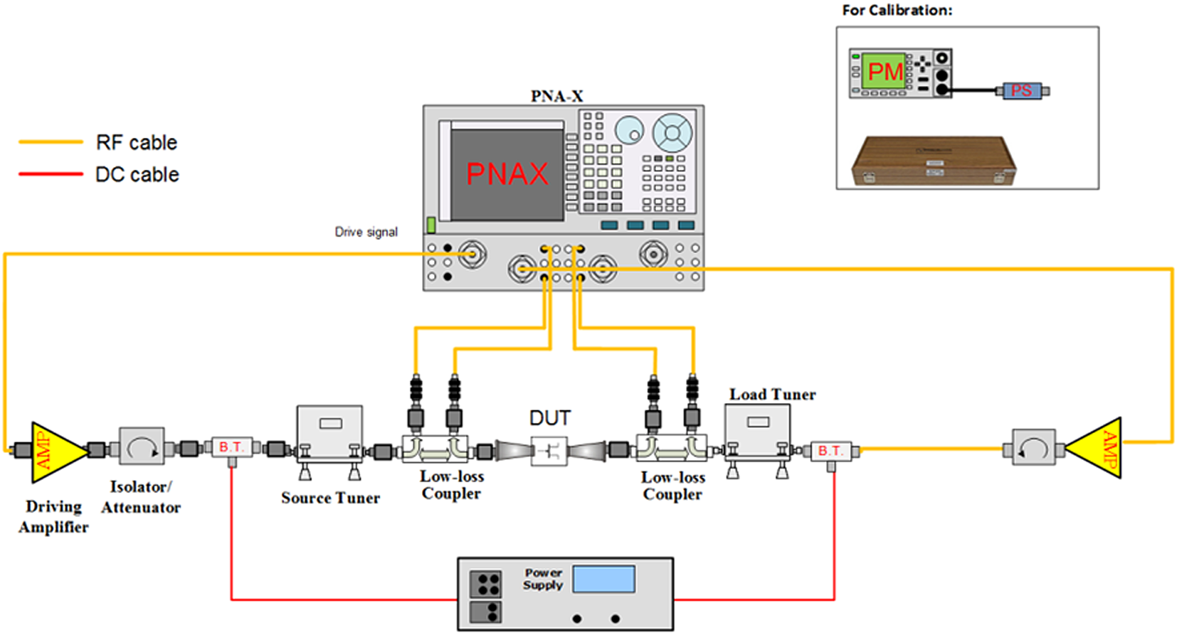
The large-signal measurements of the devices are performed using a hybrid vector-based load-pull setup with a pulse width of 33 $\mu$ s and 30% duty cycle at 35 GHz. The load impedance seen by the device under test (DUT), that is the ratio of the reflected wave by the forward-traveling wave, is limited by the losses in the system. Moreover, the optimum load impedance of the transistor changes according to the bias condition and the parasitic components, which makes it also dependent on the frequency of interest. For higher frequencies, it becomes impossible to determine the optimum load impedances of transistors using passive load-pull systems for small devices. To overcome this issue, a hybrid load-pull system is used to determine the optimum load and source impedances. The reflected wave at the output side of the device is boosted by injecting an external signal to overcome the losses of the setup in a hybrid load-pull measurement system. Therefore, impedance points that are not achievable using a conventional passive vector-based load-pull setup can be presented to the DUT to obtain optimum impedance points for maximum output power, efficiency, and gain. The schematic of the hybrid vector-based load-pull measurement setup is shown in Fig. 4. The setup utilizes PNA-X from Keysight TechnologiesFootnote 1, tuners from Maury Microwave TechnologiesFootnote 2, driving amplifiers from Exodus Advanced CommunicationsFootnote 3, and IVCAD software of AMCAD EngineeringFootnote 4.
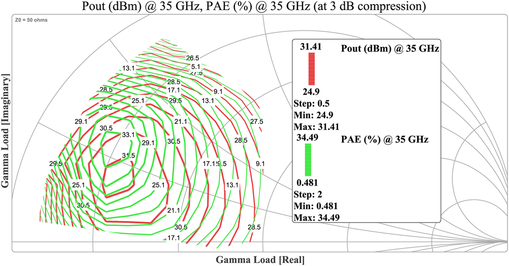
Figure 5 shows the output power and PAE contours of a $6\times 75\, \rm\mu {\rm m}$ transistor at 35 GHz at room temperature. The maximum output power of 31.4 dB is achieved at 3 dB gain compression at (12+j9) ${\rm \Omega}$
 load impedance, while the maximum PAE is 34.5% at (10+j14) ${\rm \Omega}$
 load impedance, which is close enough to the optimum impedance for the maximum output power. Large-signal measurements of various HEMTs from the same tape-out show an average output power density of 2.9 W/mm.
Output power and PAE contours of a $6\times 75\, \rm\mu {\rm m}$ HEMT at 35 GHz at 3 dB gain compression.
MMIC design considerations
Two MMIC designs, a driver amplifier (DA) and a power amplifier (PA), are completed using the GaN HEMT process to benchmark the technology at Ka-band frequencies. The designs are based on CW small-signal and pulsed large-signal characteristics of the unit transistors.
Driver amplifier MMIC design
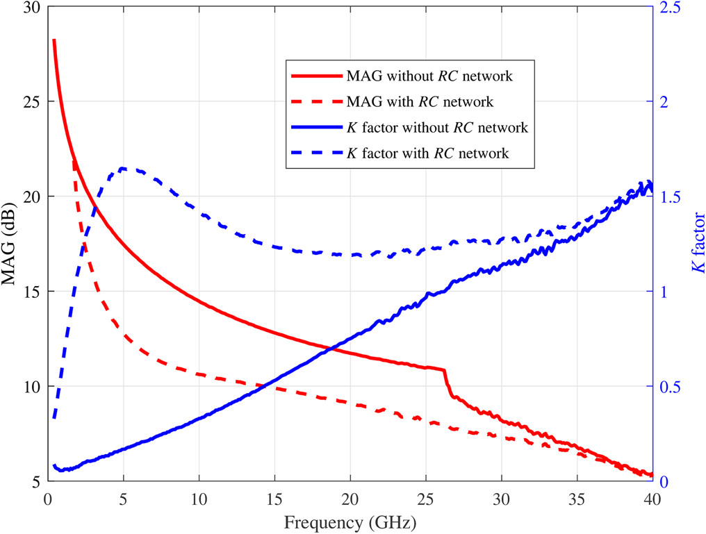
A three-stage MMIC is designed to achieve high gain with moderate output power to drive the power amplifier in an amplifier chain. Transistors with sizes of $4\times 75\, \rm\mu {\rm m}$ are used in each stage, showing a MAG of 7.9 dB at 35 GHz with 20 V drain voltage and 30 mA drain current. Transistors are stabilized unconditionally down to 1.7 GHz in even-mode using parallel RC networks with values of 120 ${\rm \Omega}$
 and 0.25 pF at their gates. The stability ($K$
 ) factor and the MAG of the transistor with and without this RC network is given in Fig. 6. Low-frequency stability is achieved with the series resistors (values of 14 ${\rm \Omega}$
 , 10 ${\rm \Omega}$
 , and 15 ${\rm \Omega}$
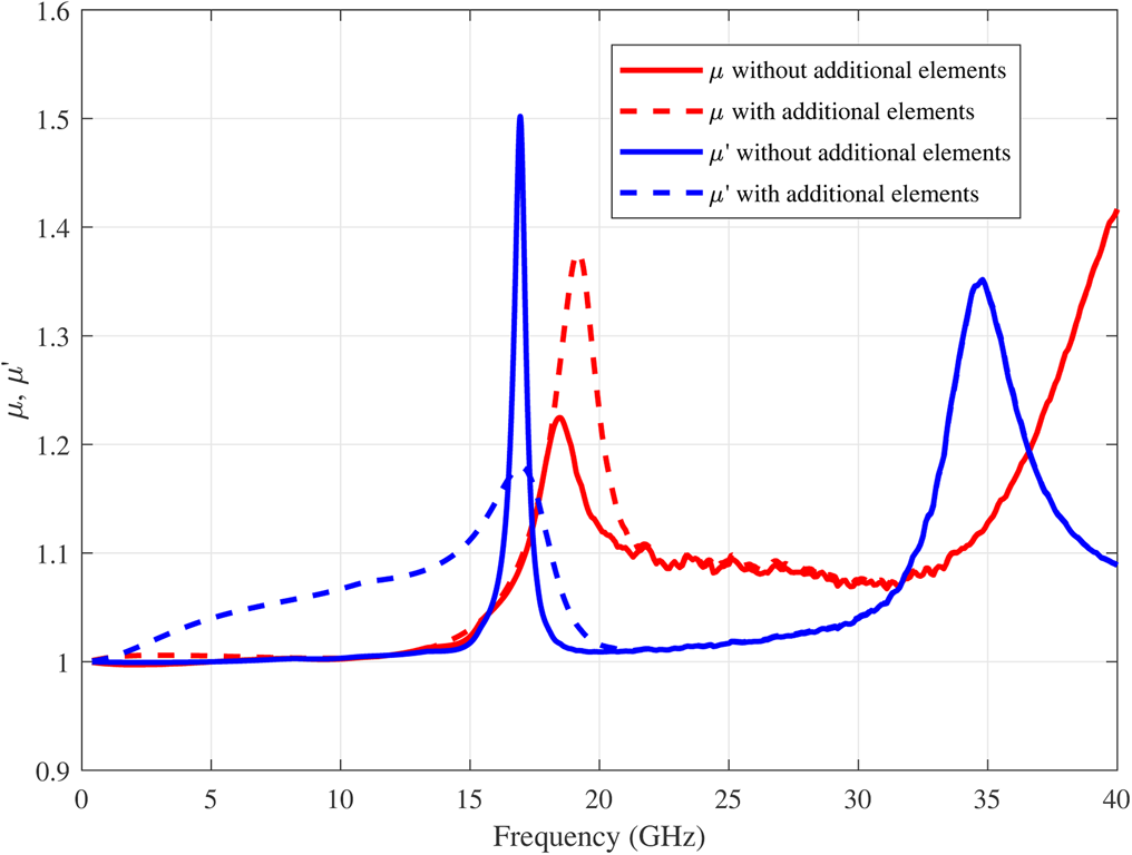
 ) and shunt RC networks at gate bias lines which are included after designing the matching networks and analyzing the stability parameters ($\mu$
 and ${\mu }'$
 ) of each stage [Reference Akoglu16]. The stability parameters are increased from below 1 to above 1 using the resistive components in the gate bias lines for all three stages. The simulation results for the second stage of MMIC are shown in Fig. 7.
MAG and $K$ factor of the $4\times 75$ $\rm\mu$
 m HEMT with and without the stability network.
Simulated even-mode stability parameters ($\mu$ and ${\mu }'$
 ) of the second stage of DA MMIC with and without additional elements on the gate bias line.
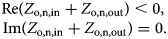
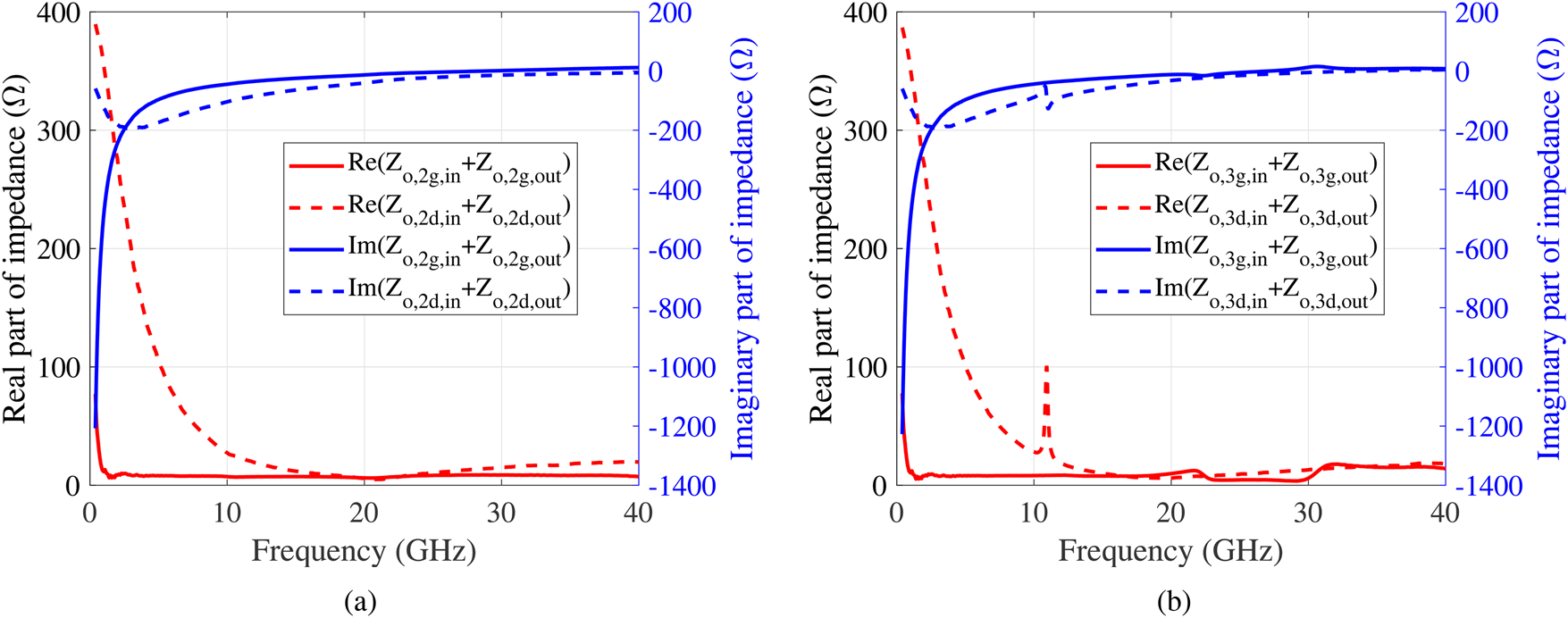
Two transistors are paralleled at the output stage, and the output matching network is optimized to get the maximum output power from these transistors. The input and interstage matching networks are designed for maximum gain from the three stages. Odd-mode stability analysis is performed by checking the oscillation conditions for each possible odd-mode excitation, as described in [Reference Freitag17] and detailed in [Reference Jankowski, Limiti and Longhi18]. The conditions considered to avoid odd-mode instability are given in (1), where the input and output impedances are calculated by splitting them into two from the parallel transistors’ gate or drain sides.
Checking the odd-mode oscillation mode of $[ + ,\; \, -]$ for the second and third stages, the odd-mode suppression resistors are placed between the second and third stage transistors to ensure odd-mode stability. The optimized values are 10 ${\rm \Omega}$
 and 5 ${\rm \Omega}$
 for the gate and drain sides of the second stage, respectively, and 12 ${\rm \Omega}$
 and 5 ${\rm \Omega}$
 for the gate and drain sides of the third stage. As shown in Fig. 8, real part of the sum of impedance values seen from the gate and drain sides of the transistors for the second and third stages are above zero for the entire simulation band, which ensures the odd-mode stability. Simulations and analysis are performed using PathWave Advanced Design System (ADS) from Keysight Technologies$^{1}$
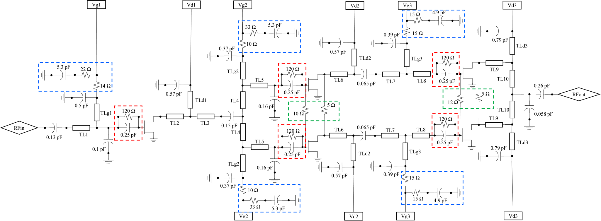
 . The chip design is finalized by adding odd-mode resistors. Figure 9 shows the schematic of the designed DA MMIC.
Stability check for $[ + ,\; \, -]$ odd excitation mode: (a) at the gate side (2g) and at the drain side (2d) of the second stage and (b) at the gate side (3g) and at the drain side (3d) of the third stage of DA MMIC.
Schematic of the designed DA MMIC, showing even-mode stability circuits at the gate (red) and at the biasing (blue) with odd-mode stability resistors (green).
Power amplifier MMIC design
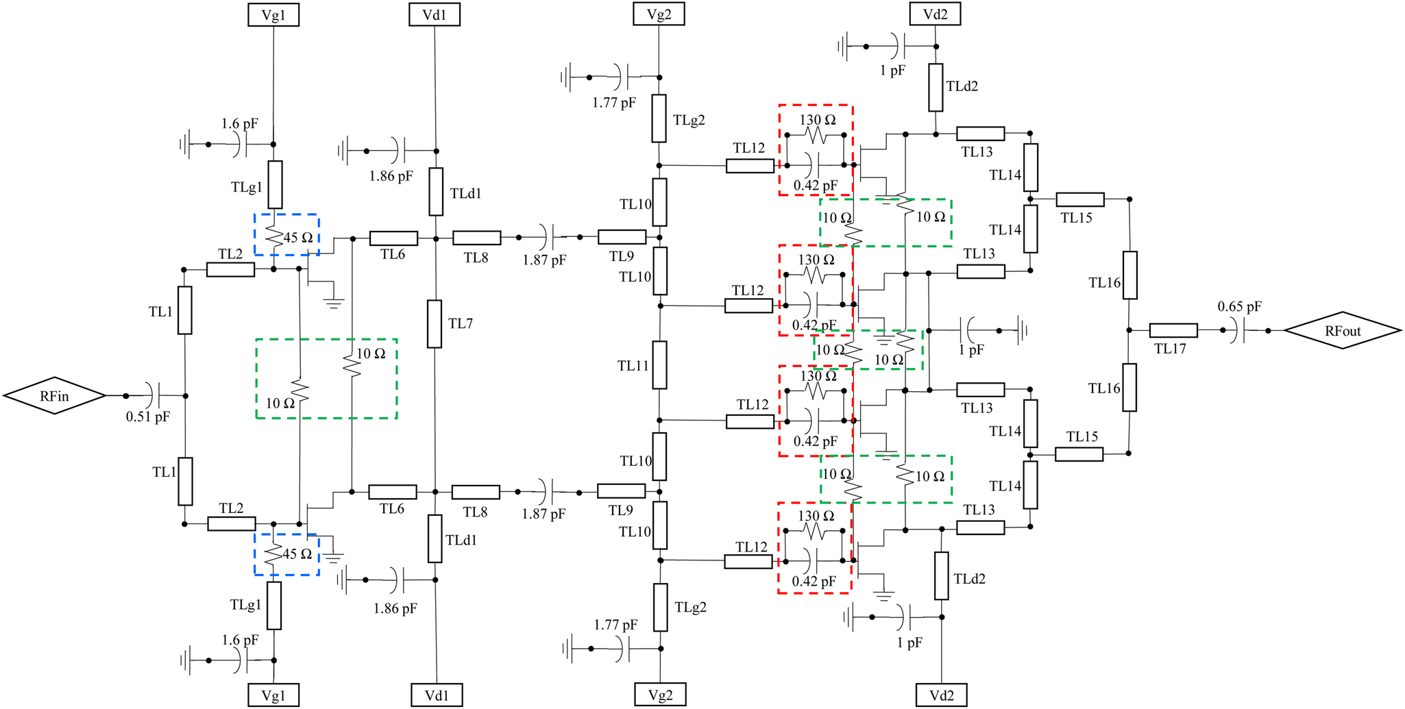
PA MMIC is designed as two-stage with a larger periphery device compared to DA MMIC to obtain a higher output power performance. The output stage of PA MMIC consists of four parallel transistors of $6\times 75\, \rm\mu {\rm m}$ . MAG of the unit transistor is 7.1 dB at 35 GHz when it is biased with 20 V drain voltage and 45 mA drain current. The drive ratio is chosen as 2:1. The load impedances of the transistors are matched for optimum efficiency together with output power at each stage. Second stage transistors are used with parallel RC networks with values of 130 ${\rm \Omega}$
 and 0.42 pF for even-mode stability, while the first stage transistors are stabilized using resistors of 45 ${\rm \Omega}$
 at the gate bias lines. Odd-mode stability is also analyzed for this MMIC considering all odd oscillation modes for both stages, e.g., $[ + ,\; \, -\; \,, - ,\; \, +]$
 , $[ + ,\; \, +\; \,, - ,\; \, -]$
 , and $[ + ,\; \, -\; \,, + ,\; \, -]$
 modes for the second stage. In the analysis, the variation of transistors throughout the MMIC is also checked by introducing phase disturbances. The odd-mode stability of the MMIC is achieved by utilizing small odd-mode resistors, approximately 10 ${\rm \Omega}$
 , between gates and drains of the parallel transistors. The schematic of the designed PA MMIC is given in Fig. 10.
Schematic of the designed PA MMIC, showing even-mode stability circuits at the gate (red) and at the biasing (blue) with odd-mode stability resistors (green).
Measurement results
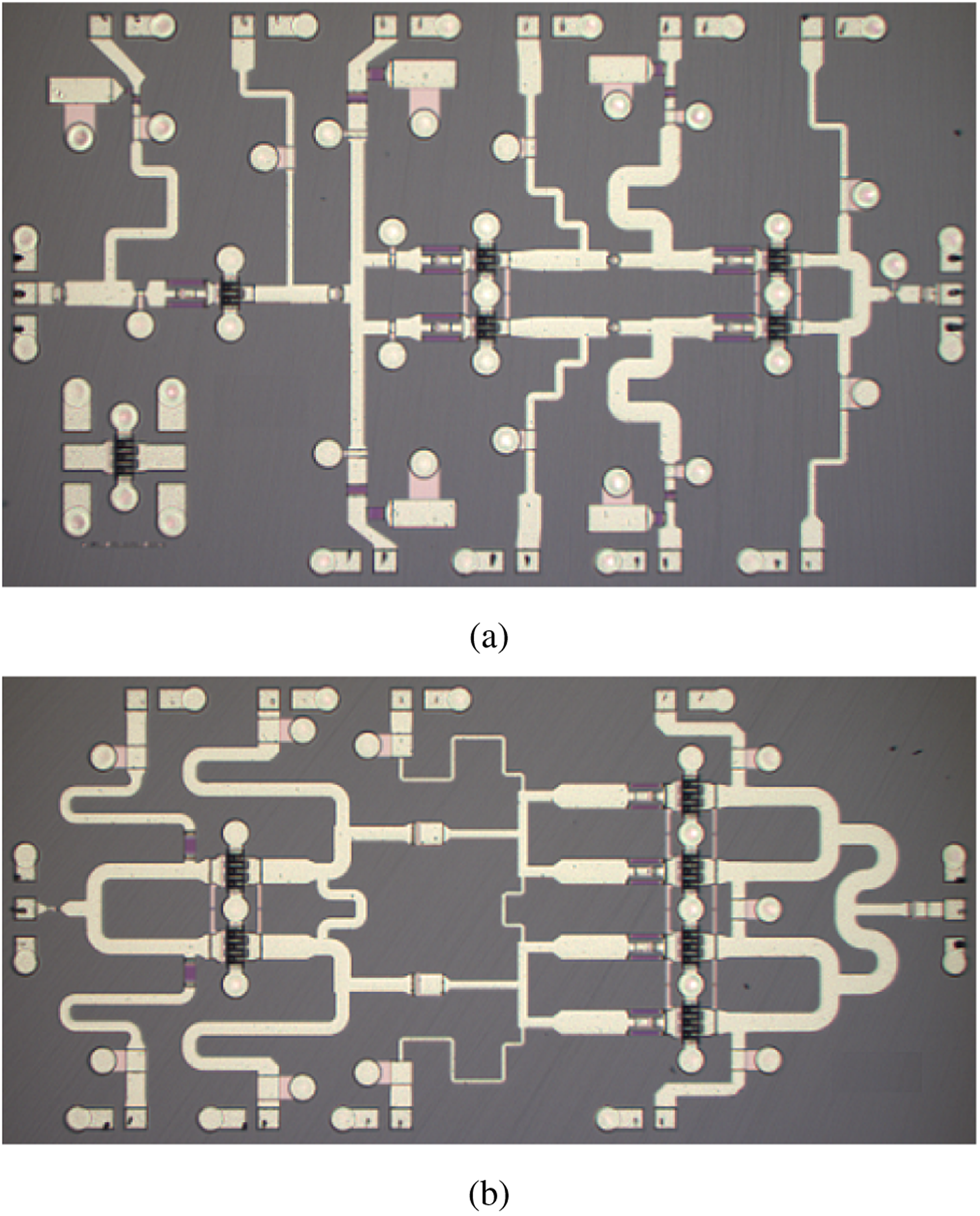
The designed MMICs are fabricated using the process described in section “GaN fabrication technology” on a 3-inch SiC wafer. The microscope images of the fabricated MMICs are given in Fig. 11. The chip size of the designed DA MMIC is $4\, {\rm mm}\times 2.4\, {\rm mm}$ , and the size of PA MMIC is smaller than $4.4\, {\rm mm}\times 2.1\, {\rm mm}$
 . Small-signal measurements are performed on-wafer under CW operation at room temperature. On the other hand, large-signal responses of MMICs are measured with a pulse width of $33\, \rm\mu {\rm m}$
 and 30% duty cycle at room temperature, again on-wafer.
Microscope images of fabricated MMICs: (a) DA MMIC (size of $4\, {\rm mm}\times 2.4\, {\rm mm}$ ) and (b) PA MMIC (size of $4.4\, {\rm mm}\times 2.1\, {\rm mm}$
 ).
).
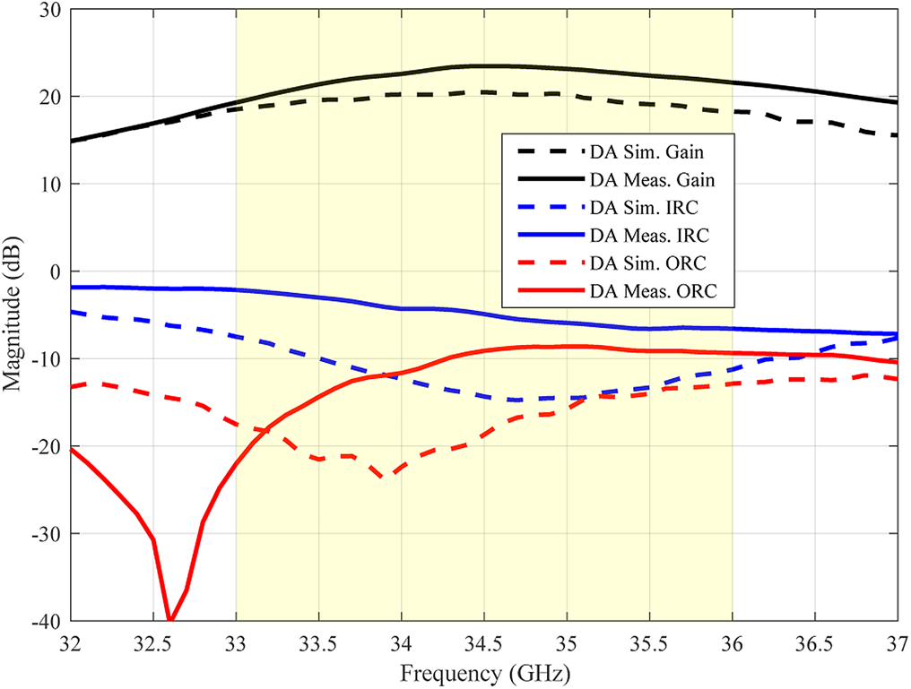
For the DA MMIC, the bias point of its each transistor is set to 20 V drain voltage with 30 mA drain current. The small-signal measurement results are shown in Fig. 12, together with the electromagnetic (EM) simulations. In the measurements, the achieved gain is between 19.3 and 23.4 dB for the desired frequency band of 33–36 GHz. Measured gain of MMIC is better than the simulated one, which is between 18.2 and 20.4 dB, while their peaks are at the same frequency. Measured input return loss (IRL) and output return loss (ORL) are better than 6 and 8.5 dB at 35 GHz, respectively. In the MMIC design, a via-hole is shared between the paralleled transistors of the output stage, while the unit transistors are characterized as single cells. This may be the reason for the difference between the simulated and measured gain, where the measured gain is higher.
Small-signal simulation and measurement results of the DA MMIC.
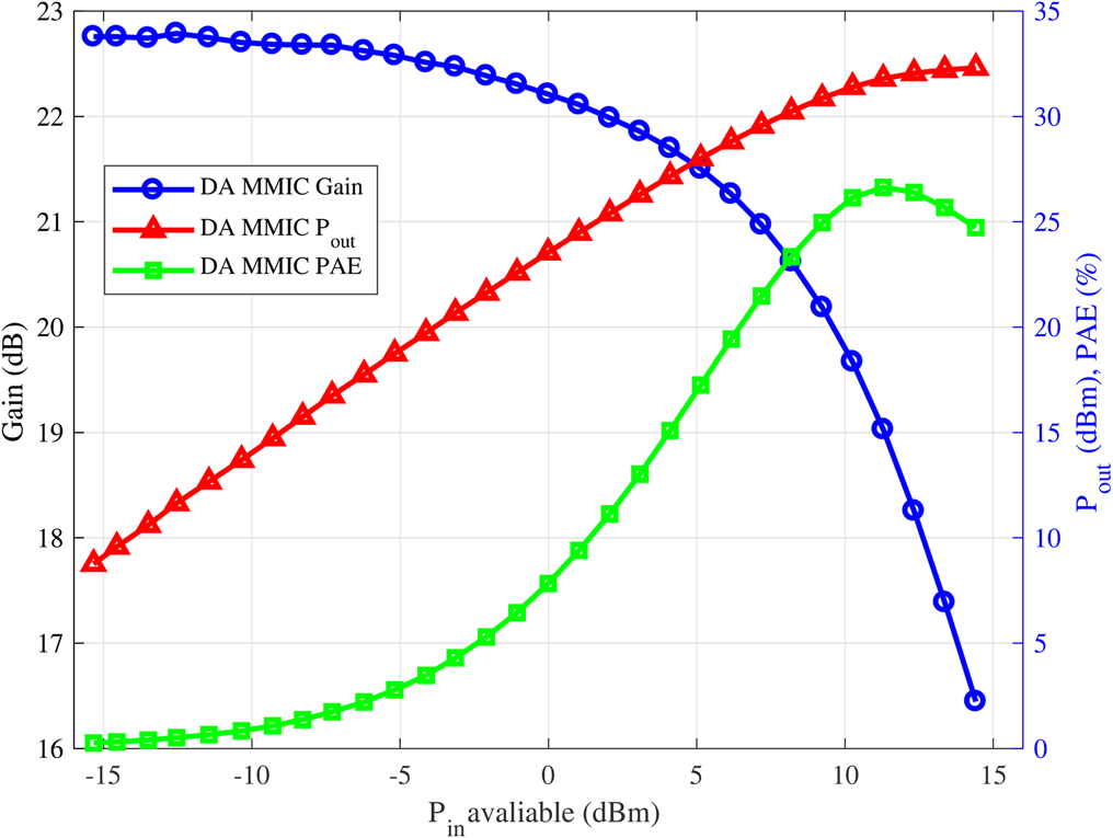
Large-signal measurement of DA MMIC is performed at 35 GHz, and the measurement results are given in Fig. 13. The DA MMIC achieves 31.9 dB output power and 26.5% PAE at 5 dB gain compression, with a large-signal gain higher than 18.8 dB. Moreover, P1 dB of the DA is measured as 26.5 dB.
Measured gain, output power, and PAE of the DA MMIC versus available input power at 35 GHz.
PA MMIC is characterized with 20 V drain voltage and 45 mA drain current for all transistors. As a two-stage circuit, the measured gain is higher than 9.9 dB for the frequency range of 33–36 GHz, with a peak of 12.9 dB. IRL and ORL are measured as better than 10 and 7 dB at 35 GHz, respectively. The reason for the lower gain in the simulations may also be the shared via-holes at the second stage, while the difference is larger compared to DA MMIC results due to the four parallel transistors of PA MMIC. Small-signal measurement and simulation results are given in Fig. 14 for the PA MMIC.
Small-signal simulation and measurement results of the PA MMIC.

Load-pull measurement of PA MMIC is also performed with a pulsed signal of 30% duty cycle at 35 GHz at room temperature. Figure 15 shows the large-signal measurement results of the PA MMIC versus available input power. The saturated output power of 35.93 dB is achieved when the gain is compressed by 7.4 dB, which is 3.91 W at 35 GHz. The maximum PAE is 26.3% at 3 dB gain compression.
Measured gain, output power, and PAE of the PA MMIC versus available input power at 35 GHz for 30% duty cycle.

The power measurements of PA MMIC are also performed with a duty cycle of 10% and under CW conditions. The output power and PAE results are compared for the three measurement conditions in Fig. 16. The output power results are 3.95 W, 3.91 W, and 3.54 W for 10% duty cycle, 30% duty cycle, and CW condition, respectively, while peak PAE values are 28.1%, 26.3%, and 25.8%, respectively. As the duty ratios of RF signal and DC supply increase, all transistors heat up more, causing a decrease in the efficiency and output power values. The efficiency improvement from 30% to 10% duty cycle is 2% at the peak, while CW condition causes only 0.5% degradation of PAE.
Measured output power and PAE of the PA MMIC for 10% duty cycle, 30% duty cycle, and CW conditions at 35 GHz.
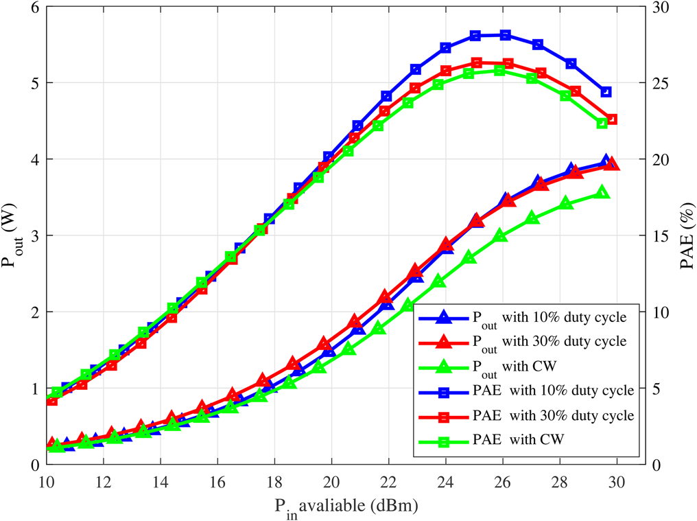
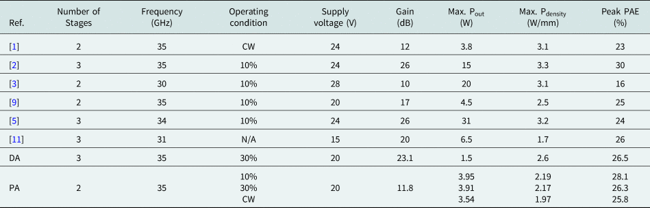
Table 1 shows the comparison to some recent MMICs based on AlGaN/GaN HEMTs at similar frequencies. The power density of each MMIC is calculated taking the total gate periphery of the output stages into account. Two MMICs of this work exhibit high PAE values, higher than 26%, with a 20 V supply voltage of 30% duty cycle. PA MMIC also shows high PAE of 28.1% with 10% duty cycle and PAE of 25.8% with CW condition. MMIC of [Reference Neininger, John, Thome, Friesicke, Brückner, Quay and Zwick11] shows a comparable PAE of 26% with the proposed MMICs, however the operating condition is not mentioned. Besides, the efficiencies of the proposed MMICs are highest after [Reference Yu, Tao and Hong2], which has a unit device with 40% PAE, while our unit device shows a maximum PAE of 34.5% at the optimum load impedance at 35 GHz. The presented MMICs also show high power densities as 2.6 W/mm and 2.2 W/mm, considering the maximum power density available from the unit devices.
A comparison of designed MMICs with other GaN-based amplifiers at Ka-band
Conclusion
Aiming Ka-band applications, two MMICs are designed and realized using NANOTAM's 0.2 $\rm\mu$ m AlGaN/GaN on SiC technology. DA and PA MMICs are optimized for 35 GHz frequency for maximum output power and efficiency, while having a bandwidth from 33 to 36 GHz in the small-signal operation. Three-stage DA MMIC has a gain higher than 19.3 dB with a variation of $\pm 2$
 dB. It exhibits 31.9 dB output power with a PAE of 26.5% at 5 dB gain compression at 35 GHz. Having an output periphery of 0.6 mm, the output power density is 2.6 W/mm for the DA MMIC. Two-stage PA MMIC shows a minimum small-signal gain of 9.9 dB for the desired frequency band, having a ripple of 3 dB. The output power and PAE of this MMIC are measured as 3.91 W and 26.3%, respectively, at 35 GHz under pulsed operation with 30% duty cycle. The total output periphery of the PA MMIC is 1.8 mm, yielding an output power density of 2.2 W/mm which is lower than that of DA MMIC because of the increasing combining loss of the output matching network while the number of devices in parallel increases. The designed and realized MMICs exhibit the capabilities of NANOTAM's 0.2 $\rm\mu$
 m AlGaN/GaN on SiC technology with high power-added efficiency values while maintaining comparable output power with recent works.
Acknowledgements
The authors would like to thank RF Design Group of NANOTAM for their help in the measurements. The authors would also like to thank the fabrication team of NANOTAM for fabricating the devices.
Conflict of interest
None.
 Busra Cankaya Akoglu received the B.S. and M.S. degrees in electrical and electronics engineering from Bilkent University, Ankara, Turkey, in 2017 and 2020, respectively. Since 2017, she has been working as a Design Engineer in the Nanotechnology Research Center (NANOTAM), Bilkent University, Ankara, and in AB-MicroNano Inc., Ankara. Her current research interests include the design and characterization of amplifiers for RF and millimeter-wave frequencies and the development of AlGaN/GaN on SiC transistors.
 Batuhan Sutbas received the B.S. and M.S. degrees in electrical and electronics engineering from Bilkent University, Ankara, Turkey, in 2016 and 2019, respectively. He is currently pursuing the Ph.D. degree at the Brandenburg University of Technology, Cottbus, Germany. From 2016 to 2019, he was a Design Engineer with the Nanotechnology Research Center (NANOTAM), Bilkent University, Ankara, and AB-MicroNano Inc., Ankara, where he was involved in the design and development of GaN-based high-power amplifier MMICs. Since 2019, he has been a Scientist with Innovations for High Performance Microelectronics (IHP), Frankfurt (Oder), Germany. His current research interests include the design of millimeter-wave radar sensors and biosensors in SiGe BiCMOS technology.
 Ekmel Ozbay received M.S. and Ph.D. degrees from Stanford University, Stanford, CA, USA, in electrical engineering, in 1989 and 1992. He worked as a postdoc at Stanford University and later as a scientist at Iowa State University, Ames, IA, USA. He joined Bilkent University, Ankara, Turkey, in 1995, where he is currently a full professor in Physics and Electrical and Electronics Engineering Departments. In 2003, he founded Nanotechnology Research Center (NANOTAM), Bilkent University, Ankara, where he leads a research group working on nanophotonics, nanoelectronics, nanometamaterials, and GaN-based devices. He is the 1997 recipient of the Adolph Lomb Medal of OSA and 2005 European Union Descartes Science award. He worked as an editor for Optics Letters, PNFA, SPIE JNP, and IEEE JQE journals. He has published 575+ articles in SCI journals. His papers have received 19500+ SCI citations with an h-index of 64. He is also the CEO of a spin-off company: AB-MicroNano Inc., which is founded to commercialize the technologies developed in NANOTAM.


 Open access