


Introduction
From multiferroics to two-dimensional electron gases (2DEGs) to strongly correlated and topological systems, much of complex oxide thin film research has been driven by interfacial phenomena for the past 20 years. Groups have demonstrated emergent oxide 2DEGs—also referred to as 2D electron systems and 2D electron liquids—due to polar/non-polar interfaces [Reference Ohtomo and Hwang1], multiferroic behavior with magnetoelectric control from interfaces between oxide ferroelectrics and ferromagnets [Reference Mundy, Brooks, Holtz, Moyer, Das, Rébola, Heron, Clarkson, Disseler, Liu, Farhan, Held, Hovden, Padgett, Mao, Paik, Misra, Kourkoutis, Arenholz, Scholl, Borchers, Ratcliff, Ramesh, Fennie, Schiffer, Muller and Schlom2, Reference Yi, Yu, Chen, Lee, He, Chu and Ramesh3], and emergent ferromagnetism [Reference Hoffman, Tung, Nelson-Cheeseman, Liu, Freeland and Bhattacharya4] as well as orbital polarization [Reference Disa, Kumah, Malashevich, Chen, Arena, Specht, Ismail-Beigi, Walker and Ahn5] due to interfacial charge transfer. Numerous groups have reviewed the novel properties that have been predicted and reported at oxide interfaces, and readers are referred to several recent review articles summarizing the state-of-the-art research in oxide thin films [Reference Coll, Fontcuberta, Althammer, Bibes, Boschker, Calleja, Cheng, Cuoco, Dittmann, Dkhil, El Baggari, Fanciulli, Fina, Fortunato, Frontera, Fujita, Garcia, Goennenwein, Granqvist, Grollier, Gross, Hagfeldt, Herranz, Hono, Houwman, Huijben, Kalaboukhov, Keeble, Koster, Kourkoutis, Levy, Lira-Cantu, MacManus-Driscoll, Mannhart, Martins, Menzel, Mikolajick, Napari, Nguyen, Niklasson, Paillard, Panigrahi, Rijnders, Sánchez, Sanchis, Sanna, Schlom, Schroeder, Shen, Siemon, Spreitzer, Sukegawa, Tamayo, van den Brink, Pryds and Granozio6, Reference Uchida and Kawasaki7, Reference Huang, Ariando, Wang, Rusydi, Chen, Yang and Venkatesan8]. Advances in thin film synthesis continue to drive the field as well. New approaches to molecular beam epitaxy (MBE) [Reference Brahlek, Gupta, Lapano, Roth, Zhang, Zhang, Haislmaier and Engel-Herbert9, Reference Suyolcu, Christiani, van Aken and Logvenov10, Reference Schlom11] and pulsed laser deposition (PLD) [Reference Groenen, Smit, Orsel, Vailionis, Bastiaens, Huijben, Boller, Rijnders and Koster12, Reference Lee, Ambrose Seo, Choi and Rouleau13] enable more precise control of cation stoichiometry than previously possible. Such approaches are highly complementary with materials characterization techniques that help to explain the physical origins of emergent phenomena in oxide thin films and interfaces.
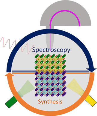
In this review, we will discuss how the reported interfacial phenomena can be examined using surface science tools—particularly in situ X-ray photoelectron spectroscopy (XPS)—in concert with film synthesis and other ex situ techniques to best understand the properties of oxide thin films, surfaces, and interfaces. This is illustrated conceptually in Fig. 1, with synthesis and spectroscopy integrated in a single vacuum system to produce a feedback loop for the study of films and interfaces. Our goal here is to introduce XPS to a synthesis-focused audience by showing how the technique can be applied to improve film growth and accelerate experimental studies of interfacial phenomena. We also demonstrate the importance of considering post-growth spectroscopy measurements during the experimental planning process, which is vital to the success of both in situ and ex situ spectroscopy measurements. Finally, a recurring theme throughout this review is that researchers must be aware of chemical effects that occur on the film surface after growth, beginning with sample cooldown all the way to atmospheric exposure and subsequent ex situ measurements. These chemical changes are often observable in XPS measurements, but it is easy to ignore their impacts on other experimental results.
Feedback loop of film synthesis and in situ XPS for the study of oxide thin films and interfaces, highlighting how interfacing in situ X-ray spectroscopy capabilities can feedback to improve the synthesis process while also providing critical information about interfacial phenomena.

Beginning with several recent examples from the literature that motivate the importance of in situ characterization, we present a brief overview of the physics of XPS and how to design experiments that best integrate thin film synthesis and in situ XPS to achieve high-quality thin films and high impact scientific results. We then present several examples of how XPS has been used in concert with film synthesis to better understand surface properties, interfacial charge transfer, electronic band alignment across a heterojunction, and non-idealities such as intermixing and off-stoichiometry. Finally, we present an overview of future opportunities that can leverage user facilities and the lessons learned from lab-based in situ studies for further breakthroughs.
Overview of complex oxide thin films and interfaces
The pursuit of a high-mobility 2DEG at complex oxide interfaces has driven research in a wide variety of materials for more than a decade. Such 2DEGs offer the promise of higher carrier concentrations than can be achieved with other materials systems, making them exciting candidates for high-speed electronics. Oxide 2DEGs also offer additional benefits over their semiconductor counterparts in that they can exhibit strong spin-orbit coupling when comprised of 5d electrons, such as those in KTaO3 [Reference Nakamura and Kimura14]. Spin-orbit coupling in a 2DEG offers an additional opportunity not available in conventional semiconductor devices. Beginning with the LaAlO3/SrTiO3 interface [Reference Ohtomo and Hwang1], many candidate materials systems have been explored. The LaAlO3/SrTiO3 system was proposed for transistors with high mobility and high carrier concentrations [Reference Herranz, Basletić, Bibes, Carrétéro, Tafra, Jacquet, Bouzehouane, Deranlot, Hamzić, Broto, Barthélémy and Fert15, Reference Hosoda, Hikita, Hwang and Bell16], spin-orbit coupled heterostructures with Rashba splitting [Reference Liang, Cheng, Wei, Luo, Yu, Zeng and Zhang17, Reference Lesne, Fu, Oyarzun, Rojas-Sánchez, Vaz, Naganuma, Sicoli, Attané, Jamet, Jacquet, George, Barthélémy, Jaffrès, Fert, Bibes and Vila18], and numerous other applications. However, controversy regarding the role of defects in the LaAlO3/SrTiO3 system [Reference Chambers, Engelhard, Shutthanandan, Zhu, Droubay, Qiao, Sushko, Feng, Lee, Gustafsson, Garfunkel, Shah, Zuo and Ramasse19, Reference Warusawithana, Richter, Mundy, Roy, Ludwig, Paetel, Heeg, Pawlicki, Kourkoutis, Zheng, Lee, Mulcahy, Zander, Zhu, Schubert, Eckstein, Muller, Hellberg, Mannhart and Schlom20, Reference Breckenfeld, Bronn, Karthik, Damodaran, Lee, Mason and Martin21] has been present for many years. As we will discuss later, XPS along with a variety of other complementary characterization techniques helped to explain the physical origin of the 2DEG in these materials [Reference Chambers, Engelhard, Shutthanandan, Zhu, Droubay, Qiao, Sushko, Feng, Lee, Gustafsson, Garfunkel, Shah, Zuo and Ramasse19, Reference Segal, Ngai, Reiner, Walker and Ahn22, Reference Chambers23].
Subsequent materials research has focused on alternative structures, including interfaces between SrTiO3 and rare-earth titanates containing a Ti3+ cation, such as in NdTiO3/SrTiO3 [Reference Xu, Droubay, Jeong, Andre Mkhoyan, Sushko, Chambers and Jalan24, Reference Xu, Ayino, Cheng, Pribiag, Comes, Sushko, Chambers and Jalan25], GdTiO3/SrTiO3 [Reference Moetakef, Cain, Ouellette, Zhang, Klenov, Janotti, Van de Walle, Rajan, Allen and Stemmer26], and LaTiO3/SrTiO3 [Reference Kim, Seo, Chisholm, Kremer, Habermeier, Keimer and Lee27, Reference Biscaras, Bergeal, Hurand, Grossetête, Rastogi, Budhani, LeBoeuf, Proust and Lesueur28]. Here, delta-doping of electrons produces the 2DEG, with the rare-earth A-site ion providing an additional electron for the system. Emergent phenomena have also been reported in these interfacial materials, including superconductivity [Reference Biscaras, Bergeal, Hurand, Grossetête, Rastogi, Budhani, LeBoeuf, Proust and Lesueur28] and ferromagnetism [Reference Moetakef, Zhang, Kozhanov, Jalan, Seshadri, Allen and Stemmer29, Reference Ayino, Xu, Tigre-Lazo, Yue, Jalan and Pribiag30]. As with the LaAlO3/SrTiO3 system, however, defects can still play a significant role, albeit in a different fashion. Various groups have reported excess oxygen content in rare-earth titanates [Reference Xu, Ayino, Cheng, Pribiag, Comes, Sushko, Chambers and Jalan25, Reference Scheiderer, Schmitt, Gabel, Zapf, Stübinger, Schütz, Dudy, Schlueter, Lee, Sing and Claessen31, Reference Aeschlimann, Preziosi, Scheiderer, Sing, Valencia, Santamaria, Luo, Ryll, Radu, Claessen, Piamonteze and Bibes32] due to either imperfect tuning of oxygen composition during growth or atmospheric exposure after growth, which has been confirmed through ex situ XPS in each case. These changes in oxygen stoichiometry can have profound impacts on material properties, changing conductivity [Reference Xu, Ayino, Cheng, Pribiag, Comes, Sushko, Chambers and Jalan25], and magnetic response [Reference Aeschlimann, Preziosi, Scheiderer, Sing, Valencia, Santamaria, Luo, Ryll, Radu, Claessen, Piamonteze and Bibes32]. When such properties are observed, it is often difficult to decouple surface chemistry and defects from emergent physical phenomena, making in situ spectroscopy valuable.
With the emerging emphasis on materials for quantum computation, materials that exhibit strong spin-orbit coupling have generated an increased interest in the oxide community as well. Work has focused on 5d transition metal oxides materials such as KTaO3 [Reference Nakamura and Kimura14, Reference King, He, Eknapakul, Buaphet, Mo, Kaneko, Harashima, Hikita, Bahramy, Bell, Hussain, Tokura, Shen, Hwang, Baumberger and Meevasana33], which exhibits the Rashba effect, and SrIrO3, which possesses stronger spin-orbit coupling. In the case of KTaO3, surface 2DEGs have been reported in ultra-high vacuum conditions from oxygen vacancies [Reference King, He, Eknapakul, Buaphet, Mo, Kaneko, Harashima, Hikita, Bahramy, Bell, Hussain, Tokura, Shen, Hwang, Baumberger and Meevasana33, Reference Santander-Syro, Bareille, Fortuna, Copie, Gabay, Bertran, Taleb-Ibrahimi, Le Fèvre, Herranz, Reyren, Bibes, Barthélémy, Lecoeur, Guevara and Rozenberg34]. Since these reports, a variety of means have been developed to produce interfacial 2DEGs in KTaO3, primarily through the introduction of polar/non-polar interfaces [Reference Thompson, Hwang, Nichols, Connell, Stemmer and Seo35, Reference Zhang, Yan, Zhang, Wang, Xiong, Zhang, Qi, Zhang, Han, Wu, Liu, Chen, Shen and Sun36, Reference Zhang, Zhang, Yan, Zhang, Zhang, Zhang, Han, Gu, Liu, Chen, Shen and Sun37]. These interfaces have exhibited such interesting properties as optically tunable Rashba effect and greater Hall mobility than analogous LaAlO3/SrTiO3 interfaces. Greater Hall mobility is due to the wider bandwidth of 5d electrons than 3d electrons [Reference Zhang, Yan, Zhang, Wang, Xiong, Zhang, Qi, Zhang, Han, Wu, Liu, Chen, Shen and Sun36]. As in previous examples, however, a more complete understanding of KTaO3 properties was gleaned from an in situ-cleaved single crystal through a combination of scanning tunneling microscopy (STM), ion scattering spectroscopy, and XPS [Reference Setvin, Reticcioli, Poelzleitner, Hulva, Schmid, Boatner, Franchini and Diebold38]. In this work, the authors showed that to compensate for the polar KTaO3 surface, a series of physical and chemical distortions occur and that the most stable surface is passivated by water adsorption, as one would expect in samples exposed to atmosphere.
Perovskite iridates are another class of 5d oxides that have generated excitement for their potential in materials systems by taking advantage of topological phenomena [Reference Kim, Jin, Moon, Kim, Park, Leem, Yu, Noh, Kim, Oh, Park, Durairaj, Cao and Rotenberg39, Reference Kim, Chen and Kee40]. SrIrO3 is a semimetallic oxide that exhibits strong spin-orbit coupling with evidence of a dimensionality driven cross-over between metallic and semiconducting behavior in ultra-thin films [Reference Nie, King, Kim, Uchida, Wei, Faeth, Ruf, Ruff, Xie, Pan, Fennie, Schlom and Shen41, Reference Schütz, Di Sante, Dudy, Gabel, Stübinger, Kamp, Huang, Capone, Husanu, Strocov, Sangiovanni, Sing and Claessen42]. In oxide heterostructures, SrIrO3 interfaces have been studied extensively for magnetic and electronic phenomena that occur due to charge transfer and electron correlations. In STO/SrIrO3 superlattices, others have shown the emergence of an energy gap at the Fermi level as the thickness of the iridate layers is reduced to ~4 u.c. [Reference Groenendijk, Autieri, Girovsky, Martinez-Velarte, Manca, Mattoni, Monteiro, Gauquelin, Verbeeck, Otte, Gabay, Picozzi and Caviglia43]. They also observed the formation of electronic energy features resembling a Dirac-cone, suggesting that topological effects occur in the ultra-thin limit. (111)-oriented SrIrO3/SrTiO3 heterostructures have also been synthesized and proposed as topological materials that exhibit the desirable honeycomb lattice for topological quantum information systems [Reference Anderson, Ryu, Zhou, Xie, Podkaminer, Ma, Irwin, Pan, Rzchowski and Eom44]. Similar (100)-oriented SrIrO3/SrTiO3 superlattices have also been shown to behave like layered Ruddelsden–Popper iridates by reducing the iridate layer to 2 unit cells (UCs) [Reference Meyers, Cao, Fabbris, Robinson, Hao, Frederick, Traynor, Yang, Lin, Upton, Casa, Kim, Gog, Karapetrova, Choi, Haskel, Ryan, Horak, Liu, Liu and Dean45]. The SrMnO3/SrIrO3 interface has also been studied through superlattice synthesis and shown to exhibit ferromagnetism due to electron transfer from Ir to Mn across the interface, leading to the anomalous Hall effect in these structures [Reference Nichols, Gao, Lee, Meyer, Freeland, Lauter, Yi, Liu, Haskel, Petrie, Guo, Herklotz, Lee, Ward, Eres, Fitzsimmons and Lee46, Reference Okamoto, Nichols, Sohn, Kim, Noh and Lee47]. LaMnO3/SrIrO3 interfaces have also demonstrated the Rashba effect, with XPS and X-ray absorption measurements confirming electron transfer from Ir to Mn [Reference Suraj, Omar, Jani, Juvaid, Hooda, Chaudhuri, Rusydi, Sethupathi, Venkatesan, Ariando and Rao48].
Strongly correlated oxides such as nickelates have been a long-standing area of interest within the oxide community, due to their potential to exhibit superconductivity that is analogous to the layered cuprates. Efforts have broadly focused on methods to induce orbital polarization in these materials to create a quasi-two-dimensional plane of nickel ions that resembles the planar cuprate structure. Groups have shown that by heterostructuring LaNiO3 into a superlattice with LaTiO3, orbital polarization can be induced to break the symmetry of the Ni e g energy levels [Reference Disa, Kumah, Malashevich, Chen, Arena, Specht, Ismail-Beigi, Walker and Ahn5, Reference Cao, Liu, Kareev, Choudhury, Middey, Meyers, Kim, Ryan, Freeland and Chakhalian49]. We will discuss ways to examine this type of charge transfer by in situ XPS later in this article. Nickelate thin films have also been shown to exhibit conductivity that is dependent on film thickness and surface termination [Reference Kumah, Disa, Ngai, Chen, Malashevich, Reiner, Ismail-Beigi, Walker and Ahn50, Reference Kumah, Malashevich, Disa, Arena, Walker, Ismail-Beigi and Ahn51, Reference Scherwitzl, Gariglio, Gabay, Zubko, Gibert and Triscone52, Reference Gray, Janotti, Son, LeBeau, Ueda, Yamashita, Kobayashi, Kaiser, Sutarto, Wadati, Sawatzky, Van de Walle, Stemmer and Fadley53, Reference Fowlie, Gibert, Tieri, Gloter, Íñiguez, Filippetti, Catalano, Gariglio, Schober, Guennou, Kreisel, Stéphan and Triscone54]. Theoretical predictions have suggested that this phenomenon is due to structural distortions in the surface layer [Reference Kumah, Malashevich, Disa, Arena, Walker, Ismail-Beigi and Ahn51], but recent work employing XPS and X-ray absorption spectroscopy (XAS) has suggested that surface oxygen vacancies could also be the cause [Reference Golalikhani, Lei, Chandrasena, Kasaei, Park, Bai, Orgiani, Ciston, Sterbinsky, Arena, Shafer, Arenholz, Davidson, Millis, Gray and Xi55]. In fact, transport models have explicitly treated the surface of LaNiO3 as having a different conductivity from the bulk of the film [Reference Fowlie, Gibert, Tieri, Gloter, Íñiguez, Filippetti, Catalano, Gariglio, Schober, Guennou, Kreisel, Stéphan and Triscone54], which would agree with the model put forward from spectroscopy. This provides a good example of the importance of considering chemical differences between the film surface and bulk when interpreting results of other physical property measurements. Recently, an infinite-layer (Nd,Sr)NiO2 nickelate heterostructure has demonstrated superconductivity for the first time [Reference Li, Lee, Wang, Osada, Crossley, Lee, Cui, Hikita and Hwang56, Reference Lee, Goodge, Li, Osada, Wang, Cui, Kourkoutis and Hwang57, Reference Hepting, Li, Jia, Lu, Paris, Tseng, Feng, Osada, Been, Hikita, Chuang, Hussain, Zhou, Nag, Garcia-Fernandez, Rossi, Huang, Huang, Shen, Schmitt, Hwang, Moritz, Zaanen, Devereaux and Lee58, Reference Zeng, Tang, Yin, Li, Huang, Hu, Liu, Omar, Jani, Lim, Han, Wan, Yang, Wee and Ariando59]. Future studies of superconducting nickelates using X-ray spectroscopy will hopefully provide further insights into the very exciting initial results.
In summary, epitaxial complex oxide thin films continue to be a fruitful area of exploration in the condensed matter physics and fundamental materials science communities. However, the complexity of the perovskite oxide materials system in terms of bulk defect tolerance and non-idealities at film surfaces and interfaces makes careful materials characterization vital to best explain the wide range of emergent properties that have been reported in oxide heterostructures. Our goal in this review is to show how XPS measurements have been used in the past to answer many of these questions such that the reader may better be able to employ the versatile technique in future studies. We also aim to provide further insights and interpretations of the current oxide interface literature, which is awash in exciting breakthroughs but also is prone to misinterpretation of XPS and complementary spectroscopy data.
Physics of XPS
The photoelectric effect is the phenomenon at the core of XPS measurements. It is so called because photons propagating through a material are absorbed by core-level and valence electrons in atoms and the resulting energy of the excited electrons is enough to overcome the electrostatic potential of the material and escape into vacuum. The photoelectric effect was first discovered in 1887 by Heinrich Hertz [Reference Hertz60], but it was not until 1905 when Albert Einstein integrated the quantization of the light into the photoelectric effect that it was fully understood [Reference Einstein61]. Einstein's discovery that the energy is E photon = hν, where h is Plank's constant and ν is the frequency of light, subsequently proved the wave-particle duality of light. Kai Siegbahn later won the Nobel Prize for his invention of XPS (then referred to as “electron spectroscopy for chemical analysis”) using hard X-rays generated by a Mo Kα1 and Kα2 source with photon energies of 17.48 and 17.37 keV, respectively [Reference Nordling, Sokolowski and Siegbahn62].
Assuming we precisely control the wavelength of light using a Rowland circle monochromator, we may determine the binding energy of an electron via the equation:
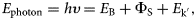 $$E_{{\rm photon}} = h\upsilon = E_{\rm B} + {\rm \Phi }_{\rm S} + E_{{\rm k}^{\prime}},$$
where the binding energy, E B, is the energy needed to bring it to the Fermi level, the material's work function, ΦS, is the energy needed to free an electron at the Fermi level and get it to vacuum, and the vacuum kinetic energy is E k’. The historical three-step model is popular to understand the physics of photoemission qualitatively, with the steps defined as: (a) optical absorption of the incoming X-ray by an atom, (b) electron transport to the surface of the material, and (c) transmission through the surface [Reference Mahan63]. We attempt to address this process briefly here and refer to the reader to texts on the physics of XPS for greater detail [Reference Briggs and Grant64, Reference Fadley and Woicik65].
XPS works by directing an X-ray beam generated by a monochromatic X-ray source onto a sample as shown in Fig. 2. The photoelectric effect causes bound electrons to be ejected out of the sample where they pass through an analyzer. This analyzer uses electron optics to select only electrons with a certain kinetic energy. By varying the settings of the optics, the XPS can sweep a range of energies. Modern XPS systems employ analyzers that allow for several electron energies to be detected simultaneously, thus making data collection more efficient [Reference Matsuda, Tóth and Daimon66, Reference Niedermaier, Kolbeck, Steinrück and Maier67, Reference Karkare, Feng, Maxson and Padmore68]. To connect the photon energy and the kinetic energy of the electrons measured by the XPS, it is best to think about the electronic band alignment diagram of XPS in Fig. 2.
(a) Energy schematic for photoemission from a thin film heterostructure. The sample stage shares a ground with the analyzer causing the Fermi levels of the sample and stage to be equal. The photoelectrons are excited by the incoming X-rays and causing them to escape from the valence and core levels of the substrate and film (left). They are collected by the electron energy analyzer (right) and the binding energy is calculated. (b) Schematic of XPS vacuum chamber configuration, showing non-monochromatic X-ray source, Rowland circle monochromator, hemispherical electron energy analyzer with lens and detector, and neutralizing electron flood gun.
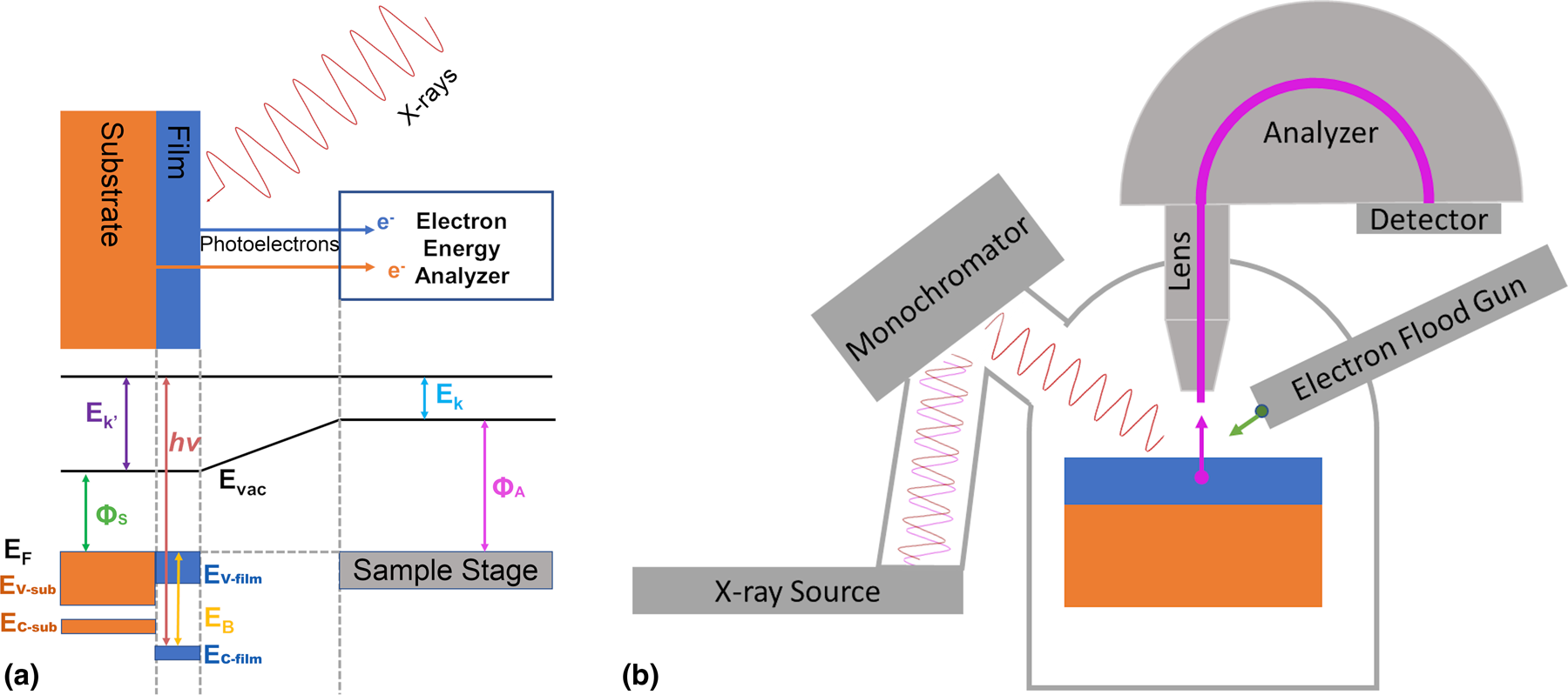
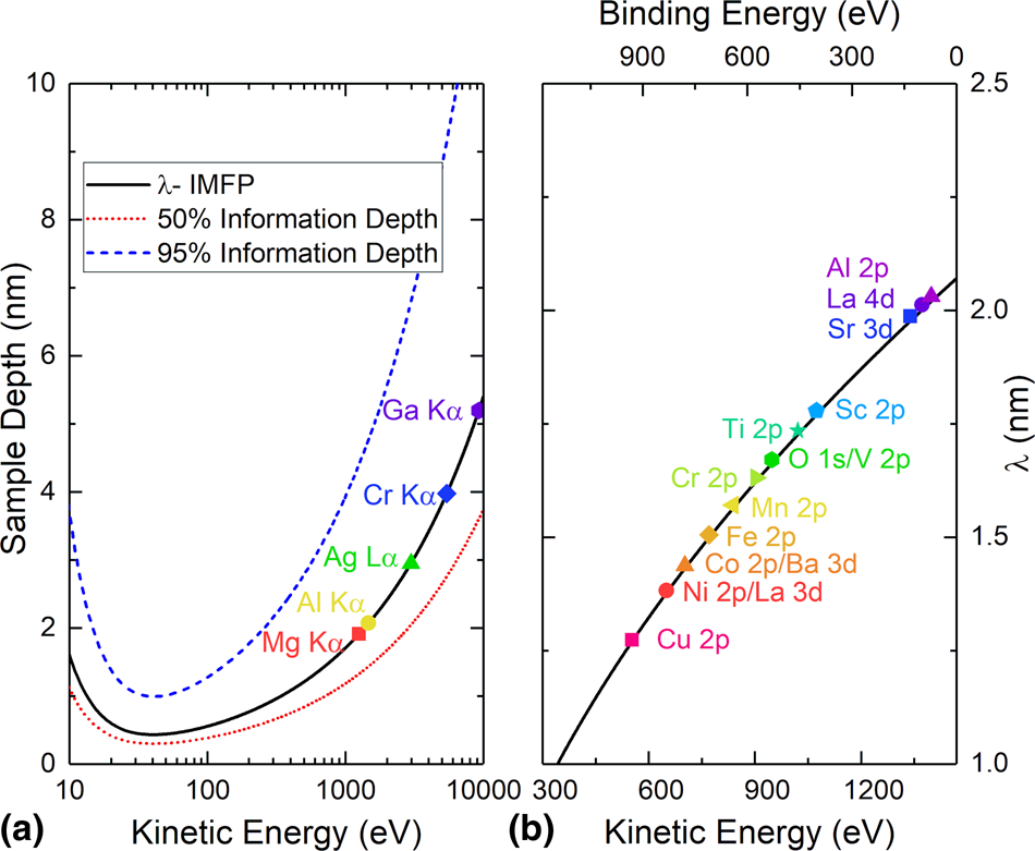
There are techniques to determine the sample's work function, but there is an immediate problem in that the kinetic energy measured by the detector, E K, is not the same kinetic energy of the emitted electrons, E K’. Due to biasing of the optics and electron energy analyzer, there is a work function of each XPS, ΦA, that relates E K to E K′. However, if the sample is mounted on a stage that shares a common ground with the XPS analyzer, then we can equate the Fermi levels of the sample and XPS. Now by looking at the band diagram, we can see that E K′ = E K + ΦA − ΦS. Substituting this into Eq. (1), we get hν = E B + E K +ΦA or E B = hν−E K−ΦA. So, by using the optics of an XPS to select and count only electrons with E K and by controlling the X-ray source frequency, we are able to calculate the binding energy of each electron excited by the photoelectric effect without knowing the sample work function, ΦS. The probability of photoelectrons escaping from the material is also sensitive to the angle of emission from a planar surface and the kinetic energy of the electron. These features are governed by the inelastic mean free path (IMFP), λ, of an electron within the material [Reference Seah and Dench69], which can be modeled by the equation:
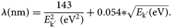 $$\lambda \lpar {{\rm nm}} \rpar = \displaystyle{{143} \over {E_{{\rm k}^{\prime}}^2 \;\lpar {{\rm e}{\rm V}^2} \rpar }} + 0.054\ast \sqrt {E_{{\rm k}^{\prime}}\lpar {{\rm eV}} \rpar }.$$
Figure 3 shows a graph of the IMFP for different X-ray sources (Fig. 3(a)) and different elemental core levels for Al Kα radiation (Fig. 3(b)). While Eqs. (1) and (2) describe the measurement of electron binding energy via XPS, separate physical phenomena govern the observation of peaks at various binding energies. Of these phenomena, the spin-orbit coupling of core-level electrons, multiplet splitting, and satellite peaks are some of the most commonly observed. However, when it comes to understanding XPS data, these are not always accurately interpreted [Reference Baer, Artyushkova, Richard Brundle, Castle, Engelhard, Gaskell, Grant, Haasch, Linford, Powell, Shard, Sherwood and Smentkowski70]. Each of these will be covered briefly in this section. Auger electrons are also detected during an XPS measurement and can be beneficial for elemental identification but are also a source of frustration if the kinetic energy of the Auger electron is close to that of an elemental core level (Fig. 3).
(a) Universal curve of the photoelectron mean free path, λ, as a function of electron kinetic energy. Dotted and dashed lines show the 50% (red, dotted) and 95% (blue, dashed) information depths in the sample for a given kinetic energy. Various lab X-ray source photon energies are labeled on the curve to show the maximum value of λ that can be achieved from that source. (b) IMFP for an Al Kα (photon energy = 1487 eV) source based on Eq. (2) for 3d transition metal 2p peaks as well as relevant peaks for Al, La, Ba, and Sr.
Because of the nature of photoelectron scattering within the crystal prior to escape, XPS measurements are inherently surface sensitive. For a given atomic species with volume density ρ, the measured intensity as a function of emission angle θ relative to the surface normal is given by:
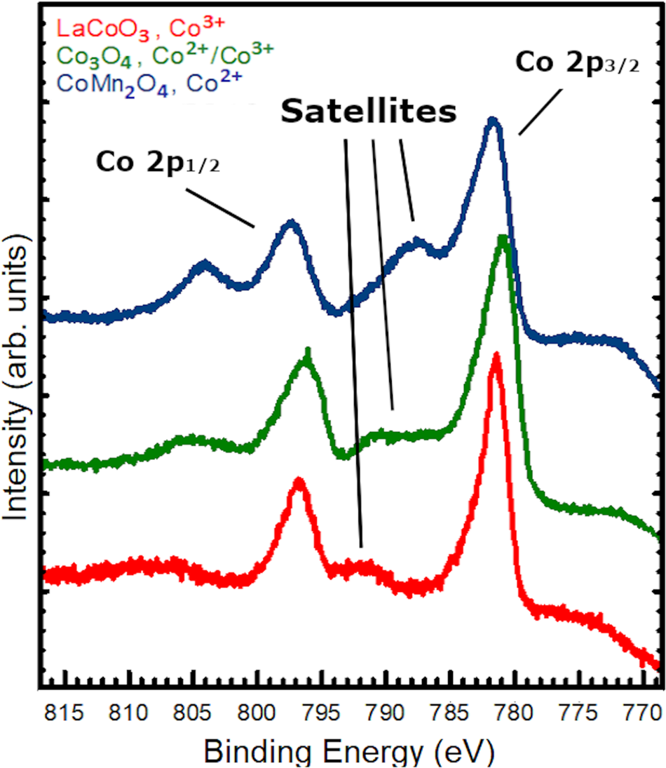
 $$I\lpar {\rm \theta} \rpar = I_0{\rm \sigma} _{{\rm n}\comma {\rm l}}T\lpar {E_{\rm k}\comma \;{\rm \theta} } \rpar A\int_0^{\rm \infty} {\rho \lpar z \rpar e^{-{z \over {{\rm \lambda} {\rm cos}\lpar {\rm \theta} \rpar }}}{\rm d}z},$$
where I 0 is the intensity for θ = 0°, σn,l is the absorption cross section for a given energy level with principal quantum number n and orbital angular momentum l, A is the measured area on the sample, z is the depth within the material, T(E k, θ) is the analyzer transmission function, and λ is the IMFP. This equation is generally simplified by assuming that the transmission function is constant over the energy values of interest and by using ratios between core-level intensities to eliminate the role of I 0 and A. For more detailed descriptions of the physics of depth sensitivity in XPS, the reader is referred to the work of Powell and Tanuma [Reference Powell, Tanuma and Woicik71]. Angle-resolved XPS measurements make clever use of the angular and depth dependence of the intensity to extract depth profiles for chemical concentrations and electronic states, which we will detail in “Combining Growth and XPS to Measure Film Quality.”
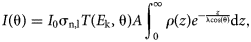
The first additional effect to consider is that of spin-orbit coupling, which is referred to as an initial state effect because it is governed by the energetic configuration of the system prior to photon absorption. Electrons with the same non-zero orbital angular momentum quantum number (i.e., p, d, f) do not all have the same binding energy. This is because spin-up and spin-down electrons have different total angular momenta. The energy shift caused by this spin-orbit coupling goes as L ∗ S, where L and S are the orbital and spin angular momentum operators, respectively. Thus, for all orbitals where l ≠ 0, there will be a splitting of the binding energy for spin-up and spin-down electrons. The two peaks correspond to the two possible values of the total angular moment of the photoelectrons, j = l ± s. For a 2p electron, the total angular momentum can take either a value of j = 1+½ = 3/2 or j = 1−1/2 = 1/2. This phenomenon can be seen in the splitting of the Co 2p into the two largest peaks of Fig. 4. Additionally, the ratio of the intensities of the peaks are seen not to be 1:1 but is instead 2:1. This is because the relative intensities are determined by the number of magnetic sub-state configurations, 2j + 1, that correspond to each j value. Knowing the expected branching ratio of the peak intensities is important when fitting XPS spectra as it allows for other effects to be distinguished from the spin-orbit coupling.
Co 2p XPS data for LaCoO3, Co3O4, and CoMn2O4 with varying Co valences.
Multiplet splitting arises from the coupling of the angular momentum of two electrons in different orbits [Reference Fadley and Shirley72]. If an atom has an unpaired core electron and an unpaired valence electron, the two electrons’ momenta can couple and result in multiple peaks. This coupling follows the L-S or Russell–Saunders coupling scheme. The peaks are separated based on the total angular momentum, j, of the coupled electrons. Spin-orbit coupling depends only on the single photoelectron emitted and thus is consistent and easily predictable effect. In the case of multiplet splitting, however, the splitting depends on both the core electron and valence electrons in the same atom. Additionally, given the presence of multiple unpaired valence electrons, the core electron can pair with any of them and each could yield a different energy shift. Multiplet splitting is commonly observed in transition metal ions that have partially filled d orbitals. For example, the valence of Mn can be determined from the multiplet splitting of the Mn 3s core level [Reference Ilton, Post, Heaney, Ling and Kerisit73], while different valences and atomic coordinations of Cr exhibit differing multiplet features [Reference Qiao, Xiao, Heald, Bowden, Varga, Exarhos, Biegalski, Ivanov, Weber, Droubay and Chambers74]. The variety of final-state coupling energies can make for highly complex spectra with several distinct energy features summing together to produce, for example, a Cr 2p 3/2 peak. In general, multiplet splitting will occur for any transition metal ion that has non-zero spin in the d band and care must be taken not to inaccurately attribute multiplet-split peaks to chemical shifts from differing formal charge.
In addition to multiplet splitting, shake-up satellite peaks occur when an atom is photo-ionized, which results in core-level hole and subsequent electronic rearrangement [Reference Brisk and Baker75]. In a shake-up shift, an electron in the valence level transitions to an unoccupied non-degenerate energy level after photoionization alters the electrostatic potential of the atom. This leaves the atom in an excited state that can be modeled using the sudden approximation and simultaneously reduces the kinetic energy of the photoemitted electron. In this way, shake-up is referred to as a final-state effect because the satellite originates from the quantum state formed in the system after the electron has been excited. This reduced kinetic energy of the photoelectron results in a satellite peak that appears to have a greater binding energy than the primary elemental core-level peak. For example, Co2+ ions exhibit a large shake-up satellite peak at higher binding energy [Reference Kim76], as can be seen in Fig. 4. The peak shape and difference in binding energy between the primary peak and the satellite can be a valuable tool for the identification of cation valence, as in the case of Co where the peak shift is fairly small between Co2+ and Co3+ but the satellite structure is markedly different. Furthermore, chemical coordination changes the selection rules for electronic energy level transitions, making shake-up satellites sensitive to ionic coordination as well as formal charge [Reference Brisk and Baker75].
A related type of final-state satellite peaks come from charge transfer between atoms. When an atom is photo-ionized, it may result in a change of the electrical structure of itself and an adjacent atom. This change in ionization and electron configuration causes a change in the potential photoelectrons feel and is again measured as a decrease in kinetic energy of the photoelectrons on an XPS spectrum. Additional satellites created by charge transfer can appear as shoulders on primary peaks or as completely distinct peaks a few eV away from the primary peak. An important thing to note is that both the j = 1/2 and j = 3/2 each have a corresponding satellite and that the ratio of intensity of 2:1 is still maintained for the satellites. Charge transfer satellites are observed in Ti 2p and O 1s spectra for materials such as SrTiO3 [Reference Kim and Winograd77].
Shake-up and charge transfer satellite peeks should not be confused with the different valence peaks. In ionic systems such as oxides, changes of the valence state of ions are expected. When ions lose or gain valence electrons, the effective nuclear charge is changed as well and can be intuitively understood using a charged-shell model introduced by Fadley et al. [Reference Fadley, Hagstrom, Klein and Shirley78]. For positively charged cations, this change is typically on the order of a few eV to higher binding energies though in some cases small enough to be difficult to resolve (~0.5 eV or less). This can be a very powerful tool to identify the bonding environment of atoms in a material, but also makes data analysis significantly more complicated and is often incorrectly presented in the literature. As an example, we show three distinct spectra for different Co valences acquired in our lab in Fig. 4. Co is an example of an ion that does not exhibit significant differences in chemical shift between the 2+ and 3+ charge state. Naïve fits to the data will generally not be sufficient to accurately determine the ratio of Co2+ to Co3+ in a mixed-valence material. Instead, readers are encouraged to refer to literature guides for rigorous fitting procedures [Reference Baer, Artyushkova, Richard Brundle, Castle, Engelhard, Gaskell, Grant, Haasch, Linford, Powell, Shard, Sherwood and Smentkowski70]. The Co L3M23M45 Auger electron also generates peak intensity at ~777 eV, accounting for the shoulder at low binding energy below the Co 2p 3/2 peak, which can complicate quantification and peak fitting.
Combining growth and XPS to measure film quality
Measuring contaminants
Epitaxial thin film research has a very low tolerance for elemental contamination. Despite engineering controls, contaminants from unknown sources sometimes make their way into samples and can either hinder data acquisition in experiments or change the physical properties of the material entirely. Surface-sensitive XPS is an excellent way to detect any unwanted element contamination, with an elemental sensitivity of <1 atomic percent. The most efficient way to measure contamination is by acquiring wide-range surveys of samples from maximum binding energy to zero. In general, it is good practice to perform surveys on every sample before performing a longer-duration, high-resolution measurement over core level and valence band regions. XPS surveys allow for a quick qualitative depiction of a sample's surface stoichiometry in addition to indicating any unexpected elemental contaminants.
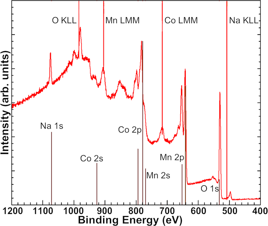
As an example, Fig. 5 is a survey of a CoMn2O4 spinel thin film sample grown in our MBE system. There are many peak features in the survey representing cobalt, manganese, and oxygen signals, but additional peaks indicate a contaminating element. Based on the position and shape of these extra features, we determined the presence of sodium on the sample surface. By inspecting surveys of samples grown at different conditions, we pinpointed the source of the sodium to the radio-frequency oxygen plasma source. After discussions with the manufacturer, the Na-contaminated quartz discharge tube was replaced with an alumina discharge tube, which has eliminated contamination. We are aware of at least one other plasma source that has also been a source of Na contamination and suggest that groups should be careful to test new plasma sources upon purchase. Given that the design employed by the manufacturer (Mantis Deposition) has been ubiquitous in the field for many years, we suspect that other groups without access to in situ XPS may have Na contamination in films without realizing. Other contaminants can be detected by XPS, such as F due to surface treatments performed on SrTiO3 with a buffered oxide etchant [Reference Chambers, Droubay, Capan and Sun79]. In this sense, the availability of in situ XPS can accelerate the calibration process for ideal growth conditions and pristine materials, making it valuable as a day-to-day diagnostic tool even when the data will not be used for publishable research.
XPS survey of CoMn2O4 thin film showing Na contamination from oxygen plasma source.
Film stoichiometry and surface termination
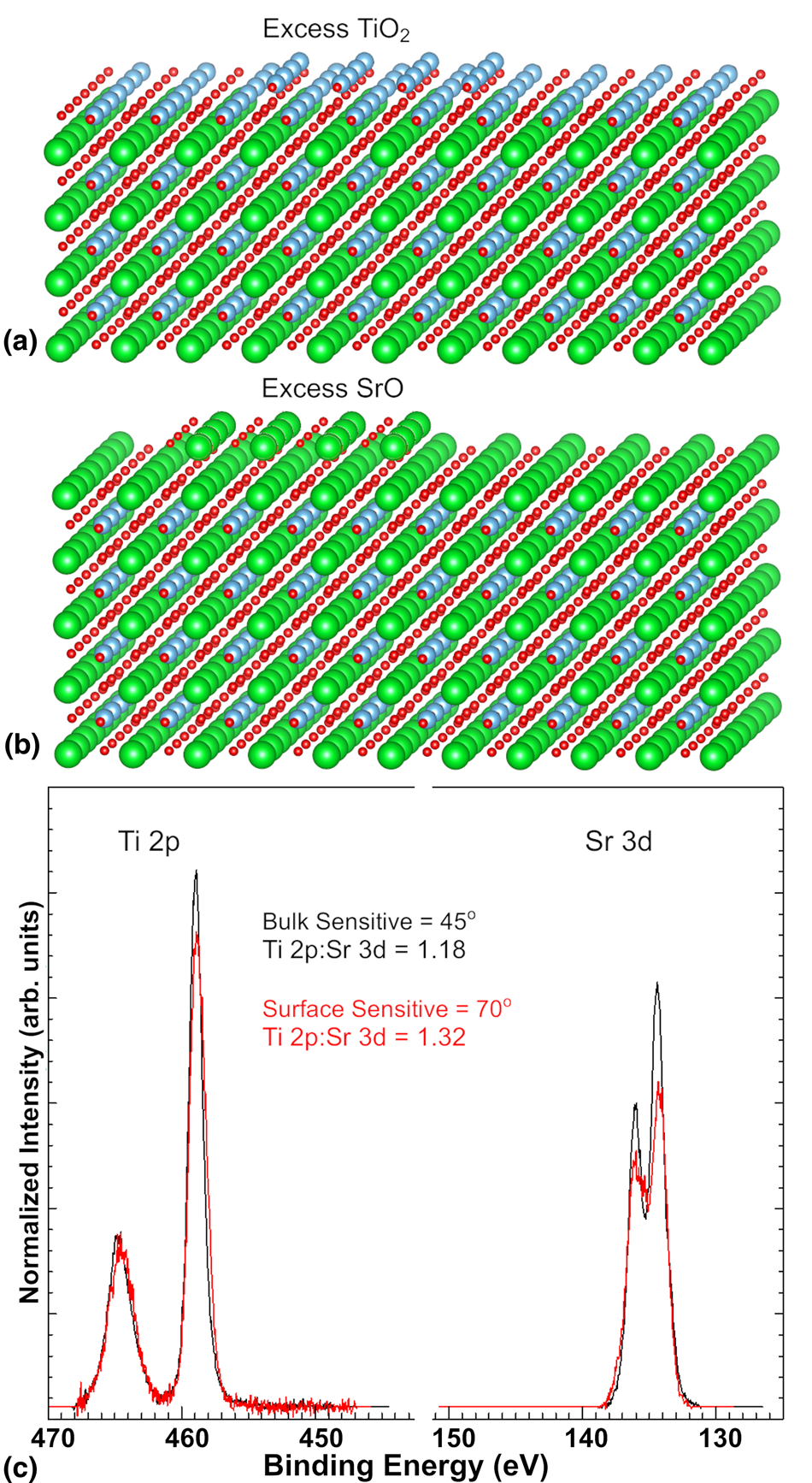
In practice, the depth sensitivity of XPS can be both a blessing and a curse. The angle-resolved XPS technique can be used to measure the surface termination of a sample, cation intermixing across an interface, and determine a depth profile of specific chemical features, providing rapid new depth-resolved insights into synthesized materials without destroying the sample through sputter etching or focused ion beam liftout for electron microscopy measurements. Conversely, the surface sensitivity of XPS means that a change as small as flipping the surface termination from TiO2 to SrO on a SrTiO3 single crystal can reduce the measured Ti:Sr peak area ratios by ~10%. This makes stoichiometry quantification for epitaxial thin films by XPS very difficult, with conventional sensitivity factors such as those used in XPS data analysis software providing very little value. Further consideration must be given to the effects of X-ray photoelectron diffraction, which can change relative peak intensities due to forward scattering of photoemitted electrons from the single crystal surface. It is generally best to benchmark the peak area ratios with a bulk-sensitive technique such as Rutherford back scattering on a film grown to produce a known surface termination. Alternatively, one can measure a single crystal reference with a known surface termination such as a treated SrTiO3 substrate [Reference Kawasaki, Takahashi, Maeda, Tsuchiya, Shinohara, Ishiyama, Yonezawa, Yoshimoto and Koinuma80]. After these initial tests, is it then possible to accurately compare peak area ratios for subsequent films to the measured area ratios from the calibrated reference sample while taking care to only compare samples with the same surface terminations.
However, despite the challenges of absolute stoichiometry quantification via XPS, we have found a convenient trick that employs in situ capabilities to accelerate the calibration process for oxide MBE growth. Given the layered nature of the perovskite crystal structure and the propensity for excess cations to reside on the film surface [Reference Lee, Luo, Tung, Chang, Luo, Malshe, Gadre, Bhattacharya, Nakhmanson, Eastman, Hong, Jellinek, Morgan, Fong and Freeland81, Reference Nie, Zhu, Lee, Kourkoutis, Mundy, Junquera, Ghosez, Baek, Sung, Xi, Shen, Muller and Schlom82], using angle-resolved XPS to determine the surface termination is generally an effective means to determine whether a perovskite oxide film has excess A-site or B-site cations even without an RBS or single crystal reference standard. The segregation is shown schematically in Figs. 6(a) and 6(b), with excess TiO2 and SrO residing on the film surface. Note that this figure is meant to schematically portray clustering of excess atoms on the film surface and not a particular surface reconstruction that might occur in such a case. The angle-resolved XPS measurement process involves comparing peak area ratios for the A-site ion to the B-site ion in a bulk-sensitive configuration near-normal emission (θ < 45°) and in a surface-sensitive configuration (θ > 70°). Such measurements can generally be completed in under an hour, making it possible to estimate whether a sample is A-site or B-site rich and recalibrate prior to additional depositions. For example, in the case of SrTiO3 films, we have seen that the ratio of the Ti 2p to the Sr 3d peak areas increases for larger values of θ if the sample is Ti-rich [Reference Thapa, Provence, Jin, Lapano, Sadowski, Brahlek and Comes83]. A comparison of one such sample is shown in Fig. 6(c). In this case, the bulk and surface-sensitive Sr 3d and Ti 2p peaks have been normalized so that the Ti 2p peaks show the same total peak area, which highlights the smaller peak area for the surface-sensitive Sr 3d peak relative to its bulk counterpart. An additional source of information is the presence of surface core-level shifts that can be measured due to incomplete coordination or OH adsorption of surface A-site ions, as has been shown for Ba-terminated BaTiO3, which shows a distinct peak at higher binding energy for the Ba 3d peak [Reference Berlich, Strauss, Langheinrich, Chassé and Morgner84]. Using these approaches while understanding the kinetics of the growth process can make in situ XPS particularly valuable for quick tuning of growth parameters sample-to-sample.
(a) Model of excess TiO2 on the film surface of TiO2-terminated SrTiO3, (b) model of excess SrO on the film surface of SrO-terminated SrTiO3, and (c) angle-resolved XPS measurement of off-stoichiometric SrTiO3 film with excess Ti cations at the film surface.
Beyond the convenience of angle-resolved XPS in the synthesis process, it has helped to explain surface-dependent phenomena in a variety of systems. We have employed angle-resolved XPS to determine for the first time that an SrO termination is more stable for stoichiometric SrTiO3 films grown by hybrid MBE [Reference Thapa, Provence, Jin, Lapano, Sadowski, Brahlek and Comes83]. Furthermore, in the case of a LaAlO3/SrTiO3 heterostructure grown on SrO-terminated SrTiO3, an unexpected AlO2 termination was observed by angle-resolved XPS, which helped to explain the absence of conductivity at the interface [Reference Singh-Bhalla, Rossen, Pálsson, Mecklenburg, Orvis, Das, Tang, Suresha, Yi, Dasgupta, Doenning, Ruiz, Yadav, Trassin, Heron, Fadley, Pentcheva, Ravichandran and Ramesh85]. Angle-resolved measurements of LaFeO3 film surfaces have also helped to explain the role of surface termination on chemical reactivity for catalytic water splitting [Reference Stoerzinger, Comes, Spurgeon, Thevuthasan, Ihm, Crumlin and Chambers86]. Despite the simplicity of angle-resolved XPS and the relatively mundane knowledge gleaned from knowing the surface termination of a thin film, there is a great deal of new physical understanding that can arise from such day-to-day measurements through in situ XPS.
Oxide surface chemistry
While understanding of the surface termination regarding perovskite AO or BO2 layers is valuable for film synthesis, it only begins to address the subtleties of surface chemistry that occur in complex oxides. The measurement of the O 1s peak can also provide valuable information to understand how the surface is passivated, a process that occurs in different ways depending on the surface polarity. It is known that water will adsorb differently depending on the AO or BO2 termination of a (001)-oriented surface [Reference Thapa, Provence, Jin, Lapano, Sadowski, Brahlek and Comes83, Reference Stoerzinger, Comes, Spurgeon, Thevuthasan, Ihm, Crumlin and Chambers86]. However, even in UHV after in situ growth, the adsorption of water on the surface can impact the electronic properties of the material. Studies that integrate XPS with atomically resolved STM are incredibly valuable in this regard to demystify some of the surface phenomena that drive emergent behavior.
As discussed above, the KTaO3 surface 2DEG is of significant interest for the Rashba splitting that is observed [Reference King, He, Eknapakul, Buaphet, Mo, Kaneko, Harashima, Hikita, Bahramy, Bell, Hussain, Tokura, Shen, Hwang, Baumberger and Meevasana33]. Through STM and XPS studies, Setvin et al. demonstrated a 2 × 1 surface reconstruction of the surface with uniform K(OH)2 coverage after water exposure [Reference Setvin, Reticcioli, Poelzleitner, Hulva, Schmid, Boatner, Franchini and Diebold38]. An OH peak on the O 1s core level at higher binding energy was reported for this case to confirm their results. Similar experiments have also been performed on layered ruthenates (Ca3Ru2O7 [Reference Halwidl, Mayr-Schmölzer, Fobes, Peng, Mao, Schmid, Mittendorfer, Redinger and Diebold87] and Sr2RuO4 [Reference Halwidl, Stöger, Mayr-Schmölzer, Pavelec, Fobes, Peng, Mao, Parkinson, Schmid, Mittendorfer, Redinger and Diebold88]) and show that water can adsorb onto the surfaces of oxides in a variety of different configurations with different binding energies relative to the metal oxide O 1s peak that is typically at ~530.0 eV. It is generally observed that films with AO termination will more readily adsorb water [Reference Setvin, Reticcioli, Poelzleitner, Hulva, Schmid, Boatner, Franchini and Diebold38, Reference Thapa, Provence, Jin, Lapano, Sadowski, Brahlek and Comes83, Reference Stoerzinger, Comes, Spurgeon, Thevuthasan, Ihm, Crumlin and Chambers86, Reference Halwidl, Stöger, Mayr-Schmölzer, Pavelec, Fobes, Peng, Mao, Parkinson, Schmid, Mittendorfer, Redinger and Diebold88], though the exact surface structure is very difficult to decipher. The effect of the adsorbed water—even after in situ growth—should not be discounted when analyzing the observed properties. For example, it is common in the literature to associate a higher binding energy peak 2.3 eV above the metal oxide binding energy with oxygen vacancies, but the origin of this peak is the subject of some controversy and it can easily be due to other surface chemistry effects that will complicate the analysis [Reference Stoerzinger, Comes, Spurgeon, Thevuthasan, Ihm, Crumlin and Chambers86].
Probing interfacial phenomena in oxide heterostructures with XPS
Interfacial chemistry and intermixing
The surface sensitivity of XPS through angle-resolved measurements can be extremely useful for the purposes of determining depth-dependent phenomena in oxide heterostructures. We have already showed the effects of surface variations and how they can be used to understand oxide film growth. However, the same techniques can be taken a step further to understand such behavior as interfacial intermixing in heterostructures and growth-induced defects such as oxygen vacancies. By varying the photoelectron emission angle to the detector and modeling the angular dependence of the relative peak areas based on the IMFP for the sample, one can construct a quantitative model of the cation or defect profile as a function of depth within a material.
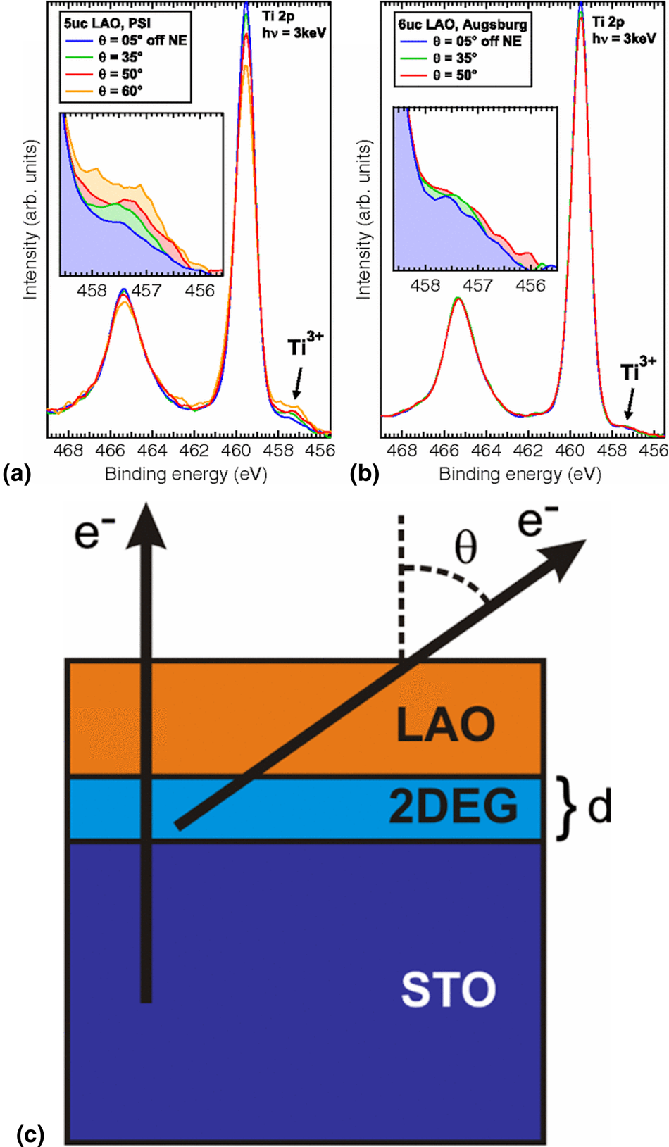
For a buried interface, angle-resolved measurements can be used to model the depth of defects or dopants. The approach has been particularly valuable in studies of polar/non-polar interfaces, where differences between the idealized physical model of an interface and the actual synthesized heterostructure have led to confusion as to the physical origin of emergent behavior. In the case of LaAlO3/SrTiO3 interfaces, angle-resolved measurements have shown that cations from the underlying SrTiO3 substrate will readily out-diffuse into the LaAlO3 film, with the degree of diffusion dependent on the cation stoichiometry of the LaAlO3 film [Reference Chambers, Engelhard, Shutthanandan, Zhu, Droubay, Qiao, Sushko, Feng, Lee, Gustafsson, Garfunkel, Shah, Zuo and Ramasse19, Reference Qiao, Droubay, Varga, Bowden, Shutthanandan, Zhu, Kaspar and Chambers89]. Through rigorous Monte Carlo modeling of the angle-resolved data, one can even estimate the cation concentration profile across the interface in a heterostructure, as Salvinelli and colleagues have demonstrated [Reference Salvinelli, Drera, Giampietri and Sangaletti90]. These measurements set the stage for further studies that confirmed that the 2DEG at these interfaces is dependent on the film stoichiometry [Reference Warusawithana, Richter, Mundy, Roy, Ludwig, Paetel, Heeg, Pawlicki, Kourkoutis, Zheng, Lee, Mulcahy, Zander, Zhu, Schubert, Eckstein, Muller, Hellberg, Mannhart and Schlom20, Reference Breckenfeld, Bronn, Karthik, Damodaran, Lee, Mason and Martin21] and thus driven in part by the formation of interfacial defects such as oxygen vacancies. Angle-resolved measurements can also be used to model the depth of distinct chemical and electronic states, such as the Ti3+ states at the LaAlO3/SrTiO3 interface. By probing the Ti 2p core level of samples using ex situ hard X-ray photoemission, Sing et al. developed a model of the thickness of the 2DEG in UCs to show that it was confined to a single UC at the surface of the SrTiO3 substrate [Reference Sing, Berner, Goß, Müller, Ruff, Wetscherek, Thiel, Mannhart, Pauli, Schneider, Willmott, Gorgoi, Schäfers and Claessen91]. The results from this work are shown in Fig. 7. Other angle-resolved studies have shown that oxygen vacancies in SrTiO3-based heterostructures are localized at the interface [Reference Chen, Bovet, Trier, Christensen, Qu, Andersen, Kasama, Zhang, Giraud, Dufouleur, Jespersen, Sun, Smith, Nygård, Lu, Büchner, Shen, Linderoth and Pryds92, Reference Saghayezhian, Wang, Guo, Zhu, Plummer and Zhang93].
Ti 2p core-level data showing Ti3+ intensity at the LaAlO3/SrTiO3 interface for two different samples (a and b). Variation with angle in (a) shows that Ti3+ is non-uniformly distributed in comparison to the uniform distribution in (b). (c) Schematic of angle-resolved XPS measurement of 2DEG location. Reprinted figure with permission from Sing et al. [Reference Sing, Berner, Goß, Müller, Ruff, Wetscherek, Thiel, Mannhart, Pauli, Schneider, Willmott, Gorgoi, Schäfers and Claessen91]. Copyright 2009 by the American Physical Society.
In the case of a 6 UC SrTiO3–3 UC LaCrO3 superlattice, in situ angle-resolved XPS measurements were used to determine the degree of Cr out-diffusion into the topmost SrTiO3 layer [Reference Comes, Spurgeon, Kepaptsoglou, Engelhard, Perea, Kaspar, Ramasse, Sushko and Chambers94]. The resulting data were compared with a model with differing degrees of Cr intermixing to estimate the Ti–Cr concentration profile across the B-site of the superlattice. Interfacial models were constructed to represent differing percentages of B-site cation intermixing and contributions to the overall Cr 2p and Ti 2p peak intensities were estimated by accounting for the IMFP in the material for each layer. The resulting estimates showed that there is significant intermixing of Ti across the interface, with approximately 25% of the middle B-site ions in the LaCrO3 layer occupied by Ti ions. Critically, the model agreed very well with extracted concentration profiles from STEM-EELS measurements, as shown in Fig. 8 [Reference Comes, Spurgeon, Kepaptsoglou, Engelhard, Perea, Kaspar, Ramasse, Sushko and Chambers94].
(a) Angle-resolved XPS Cr 2p:Ti 2p peak ratio with models assuming various degrees of intermixing (0° is normal to the film surface), (b) concentration profile for the 35%-intermixing model, and (c) STEM-EELS integrated signal profile throughout superlattice determined using MLLS fitting of the Cr L23 edge and the background-subtracted peak area of the Ti L23 edge. The signal has been normalized to the substrate. Reprinted with permission from Comes et al. [Reference Comes, Spurgeon, Kepaptsoglou, Engelhard, Perea, Kaspar, Ramasse, Sushko and Chambers94]. Copyright 2017 American Chemical Society.

Band alignment and potential gradients
Semiconductor heterostructures are key to modern-day electronics, and numerous oxide heterojunctions have been pursued for their potential applications. The performance of these heterostructures can be engineered by manipulating valence and conduction band offset at the interface. It is crucial to understand this band offset to accurately predict and manipulate the behavior of thin film heterostructures.
There are different schemes to determine the band offset experimentally such as ultra-violet spectroscopy, internal photoemission spectroscopy, and XPS. Band offset determination via XPS has been used extensively. Unlike other methods, XPS is sensitive to details at the interface such as changes in valence and chemical intermixing and thus is often preferred over other methods. The XPS approach to valence band alignment determination was first introduced by Kraut et al. [Reference Kraut, Grant, Waldrop and Kowalczyk95]. It is based on the premise that the energy difference between a core level and valence band maximum (VBM) is an intrinsic property and remains constant independent of any formation of a heterostructure. Any change in the binding energy of the VBM will change the core level equally, making the energy of the core-level peak a good proxy for the VBM. This becomes important when measuring a thin film heterostructure, as the valence band region will now be the convolution of two or more distinct materials, while appropriately chosen core levels can still be measured easily and fit repeatably. The precision of this method lies in the measurement of core level and valence band maxima binding energies from reference samples for each material in a heterojunction. This can be accomplished using a single crystal reference or carefully grown film that is sufficiently thick such that the underlying substrate does not contribute any signal to the data. With the two reference samples and one more heterojunctions under examination, at least three samples are needed to apply this approach.
Using their data, Kraut et al. [Reference Kraut, Grant, Waldrop and Kowalczyk95] determined the VBM by fitting valence band spectra with the theoretical valence band density of states. However, fits involving a linear extrapolation of the leading edge of the valence band spectra to the zero-level backgrounds have been found to be as accurate and require much less effort. Various refinements to this approach over the years for oxide heterostructures have been proposed [Reference Chambers, Du, Comes, Spurgeon and Sushko96, Reference Chambers, Droubay, Kaspar and Gutowski97]. A diagram illustrating Kraut's method is shown in Fig. 9. The valence band and conduction band offset are calculated as
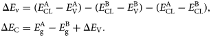 $$\eqalign{\Delta E_{\rm v} &= \lpar {E_{{\rm CL}}^{\rm A} -E_{\rm V}^{\rm A} } \rpar -\lpar {E_{{\rm CL}}^{\rm B} -E_{\rm V}^{\rm B} } \rpar -\lpar {E_{{\rm CL}}^{\rm A} -E_{{\rm CL}}^{\rm B}} \rpar, \cr \Delta E_{\rm C} &= E_{\rm g}^{\rm A} -E_{\rm g}^{\rm B} + \Delta E_{\rm V}.}$$
Schematic rendering of method to measure band alignment in XPS via core-level binding energies. E CL refers to core-level binding energy, E V refers to the VBM, and E C refers to the conduction band minimum for materials A and B. By measuring these values for thick films or single crystal references, one can then determine the value of ΔE V for a heterostructure by measuring the difference E CLA – E CLB.
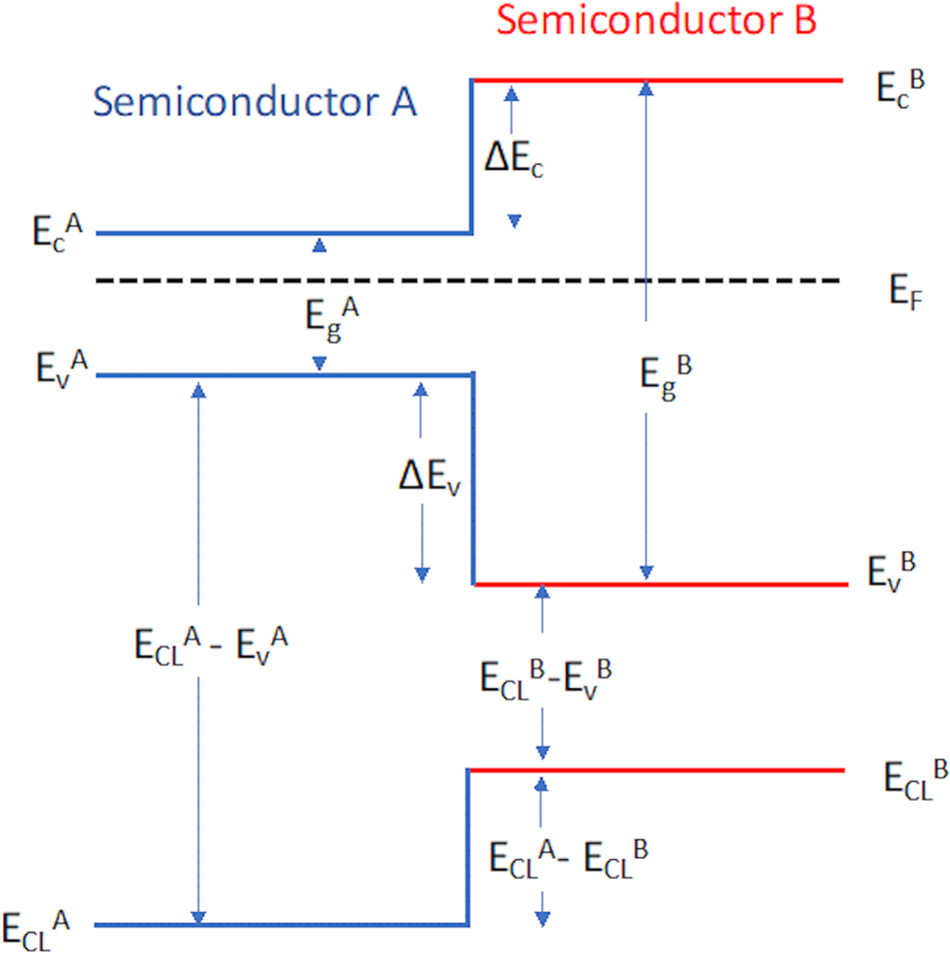
The core-level peaks and valence band reference spectra should be acquired with high energy resolution, as the uncertainty of the measurement of the core-level peak position will propagate into the band offset calculation. The choice of peaks that have a narrow intrinsic width and are easier to fit repeatably is thus very important.
The LaAlO3/SrTiO3 interface has been widely studied for its unusual transport properties. The properties can be attributed to an effective 2DEG at the interface. The origin of this 2DEG has been the source of great controversy, with some attributing it to the polar discontinuity [Reference Ohtomo and Hwang1, Reference Sing, Berner, Goß, Müller, Ruff, Wetscherek, Thiel, Mannhart, Pauli, Schneider, Willmott, Gorgoi, Schäfers and Claessen91] and others to defect-driven phenomena [Reference Chambers, Engelhard, Shutthanandan, Zhu, Droubay, Qiao, Sushko, Feng, Lee, Gustafsson, Garfunkel, Shah, Zuo and Ramasse19, Reference Warusawithana, Richter, Mundy, Roy, Ludwig, Paetel, Heeg, Pawlicki, Kourkoutis, Zheng, Lee, Mulcahy, Zander, Zhu, Schubert, Eckstein, Muller, Hellberg, Mannhart and Schlom20, Reference Breckenfeld, Bronn, Karthik, Damodaran, Lee, Mason and Martin21, Reference Chambers23]. Owing to its high precision in measuring core levels and VBMs, and subsequently the valence band and conduction band offsets, XPS has been a powerful tool in studying this heterostructure interface. Additionally, XPS data can be modeled to estimate the potential gradient across the film.
Multiple groups have used XPS to study the LaAlO3/SrTiO3 interface grown by both MBE [Reference Segal, Ngai, Reiner, Walker and Ahn22] and PLD [Reference Chambers, Engelhard, Shutthanandan, Zhu, Droubay, Qiao, Sushko, Feng, Lee, Gustafsson, Garfunkel, Shah, Zuo and Ramasse19, Reference Qiao, Droubay, Shutthanandan, Zhu, Sushko and Chambers98, Reference Drera, Salvinelli, Brinkman, Huijben, Koster, Hilgenkamp, Rijnders, Visentin and Sangaletti99] with different film thicknesses and terminations for possible explanations for the origin of the interface's 2DEG. In one such work, Segal et al. confirmed the metal–insulator interface transition with 4 UC-thick LaAlO3 on a TiO2-terminated surface [Reference Segal, Ngai, Reiner, Walker and Ahn22]. Many studies suggest that the 2DEG at the interface stems from an electronic reconstruction due to polar discontinuity (LAO has alternating positive and negative atomic layers), known as the “polar catastrophe” [Reference Sing, Berner, Goß, Müller, Ruff, Wetscherek, Thiel, Mannhart, Pauli, Schneider, Willmott, Gorgoi, Schäfers and Claessen91]. From the experimental band offset and band gap, Segal et al. calculated that a potential gradient of 1.15 ± 0.06 at a 4 UC thickness is required for the polar catastrophe to occur, whereas the measured potential gradient at 4 UCs was much less than the required value. This means that other phenomena such as oxygen defects, lattice distortion, and cation mixing at the interface must be investigated to explain this unique behavior at the interface. In this way, XPS has helped to further elucidate the origin of 2DEG at the LAO-STO interface, which was later shown to be strongly dependent on LaAlO3 cation off-stoichiometry [Reference Warusawithana, Richter, Mundy, Roy, Ludwig, Paetel, Heeg, Pawlicki, Kourkoutis, Zheng, Lee, Mulcahy, Zander, Zhu, Schubert, Eckstein, Muller, Hellberg, Mannhart and Schlom20, Reference Breckenfeld, Bronn, Karthik, Damodaran, Lee, Mason and Martin21].
Other studies of interfaces where both sides of the heterojunction are comprised of band insulators with the VBM comprised of O 2p-derived electronic states, have generally shown small valence band offsets of ~0.5 eV or less [Reference Giampietri, Drera and Sangaletti100]. This includes the SrTiO3/(La,Sr)(Al,Ta)O3 interface [Reference Comes, Xu, Jalan and Chambers101], the SrZrO3/SrTiO3 interface [Reference Schafranek, Baniecki, Ishii, Kotaka, Yamanka and Kurihara102], and the BaSnO3 interface with both SrTiO3 and LaAlO3 [Reference Chambers, Kaspar, Prakash, Haugstad and Jalan103]. The small valence band offset can generally be attributed to the condition that the O 2p energy level is continuous across the heterojunction [Reference Zhong and Hansmann104], which will be discussed in more detail shortly.
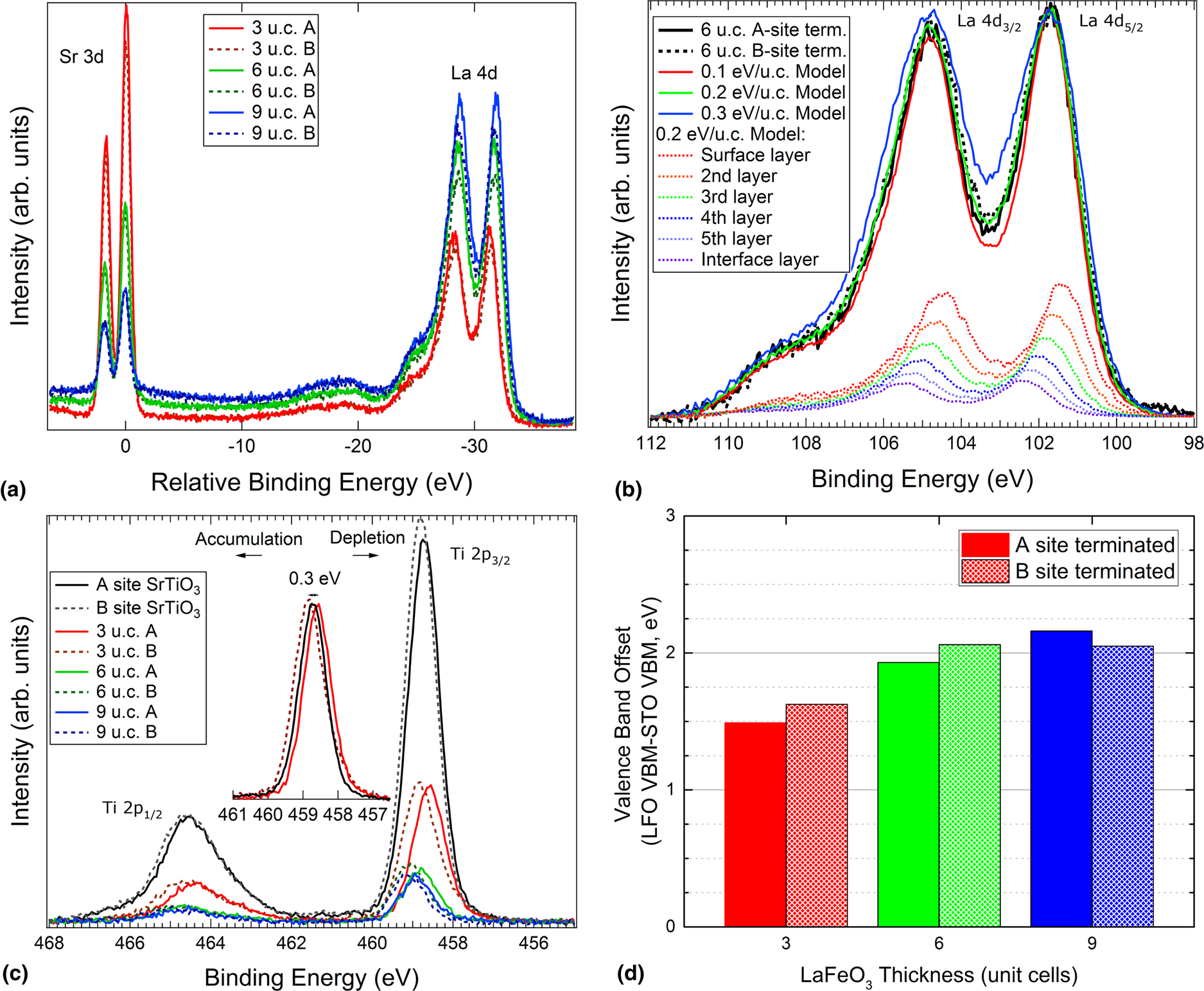
Unlike the isoelectronic interfaces where O 2p states form the top of the valence band on both sides of the heterojunction, interfaces between Mott–Hubbard and band insulators offer additional degrees of freedom. For example, the LaFeO3/n-SrTiO3 system also creates a polar non-polar interface and is studied for its photocatalytic applications [Reference Nakamura, Kagawa, Tanigaki, Park, Matsuda, Shindo, Tokura and Kawasaki105, Reference Nakamura, Mashiko, Yoshimatsu and Ohtomo106, Reference Comes and Chambers107, Reference Xu, Han, Rice, Jeong, Samant, Mohseni, Meyerheim, Ostanin, Maznichenko, Mertig, Gross, Ernst and Parkin108]. Nakamura et al. [Reference Nakamura, Kagawa, Tanigaki, Park, Matsuda, Shindo, Tokura and Kawasaki105] studied the interface-induced polarization of LaFeO3/Nb-doped SrTiO3 heterostructures and observed novel shift current that suggested the polarization direction switches for different substrate terminations (SrO and TiO2). This would mean that potential gradients took on opposite signs for different terminations and suggested that changes in polarization are responsible for observed photoconductivity. Subsequent studies of LaFeO3/Nb-doped SrTiO3 junctions with varying LaFeO3 film thicknesses (3,6 and 9 UCs) and different substrate terminations (SrO and TiO2) grown using MBE and characterized by in situ XPS helped to address these questions [Reference Comes and Chambers107]. These studies found an increase in separation between core levels (La 4d and Sr 3d) with increases in film thickness, clearly indicating that band offset and built-in potential change with thickness. In addition, by modeling the broadening of the La 4d peaks with different film thicknesses and terminations, it was possible to estimate the potential gradient across the film. Contrary to the reported interface-induced polarization [Reference Nakamura, Kagawa, Tanigaki, Park, Matsuda, Shindo, Tokura and Kawasaki105, Reference Nakamura, Mashiko, Yoshimatsu and Ohtomo106], the results indicated that the interface termination had only a small impact on the band alignment and the built-in potential gradient [Reference Comes and Chambers107]. The models are shown in Fig. 10. The chemical instability of the SrO/FeO2 interface has been proposed as a likely explanation for these results [Reference Spurgeon, Sushko, Chambers and Comes109]. These results were subsequently matched by first-principles band alignment models of the interface [Reference Xu, Han, Rice, Jeong, Samant, Mohseni, Meyerheim, Ostanin, Maznichenko, Mertig, Gross, Ernst and Parkin108].
(a) Sr 3d and La 4d core-level spectra for the family of heterostructures, shifted to align the Sr 3d peaks; (b) model of La 4d peak broadening in the 6 u.c. films; (c) Ti 2p core-level spectra for each film and substrate, with the inset showing the peak shifts; (d) valence band offsets determined from the core-level spectra for each heterojunction. Reprinted figure with permission from Comes and Chambers (2016) [Reference Comes and Chambers107]. Copyright 2016 by the American Physical Society.
Interfacial charge transfer
As in modulation-doped semiconductor heterostructures, interfacial charge transfer is an important tool in complex oxides to induce novel magnetic and electronic functionalities that do not occur in equilibrium. One of the crucial parameters to determine the charge transfer probability is the charge transfer gap. In most of the cases, the charge transfer gap is determined by band splitting of B-site cations or the band gap between B-site cations and fully occupied O 2p bands, while A-site cations have a less significant role. Predicting charge transfer is not straight forward in oxide heterostructures since the classic band alignment principle is not strictly followed as in the case of semiconductors. A modified rule is based on the continuity of states of the O 2p band across the interface and allows for a qualitative prediction of band alignments and charge transfer in complex oxide heterostructures [Reference Zhong and Hansmann104]. In cubic oxides, the local energy of O 2p states relative to the Fermi level, ɛ p−E F, has been proposed to be the deterministic factor to tune the direction of charge transfer from one complex oxide to another. Generally, electron transfer favors electron flow from lower (more negative) ɛ p−E F to higher. The classic semiconductor rule is shown in Fig. 11(a), while the modified rule for oxides is shown in Figs. 11(b)–11(e). This rule led to the development of alternative computational methods to predict charge transfer that have been shown to be effective in recent years.
(a) Conventional model for semiconductor band alignment based on aligning the vacuum level for constituent materials; (b) preliminary band alignment based on the alignment of O 2p states prior to charge transfer; (c) reconstructed band alignment after charge transfer equilibration of the Fermi energy level; (d) schematic model of ABO3/AB'O3 interface emphasizing continuity of O 2p electronic states; (e) summary of bulk ɛp (filled symbols) and ɛd (empty symbols) with respect to the Fermi level (E F = 0) for different SrBO3 (solid line) materials, with 3d (black), 4d (red), and 5d (blue) elements. The simple criterion for the direction of the charge transfer at the ABO3/AB′O3 interface is that the component with lower (more negative) ɛp−E F will donate electrons across the interface to the opposite material. Also plotted is LaBO3 (dashed line) for B=3d, for estimates for ABO3/A′BO3 interfaces. Adapted under Creative Commons Attribution 3.0 License from Zhong and Hansmann [Reference Zhong and Hansmann104].
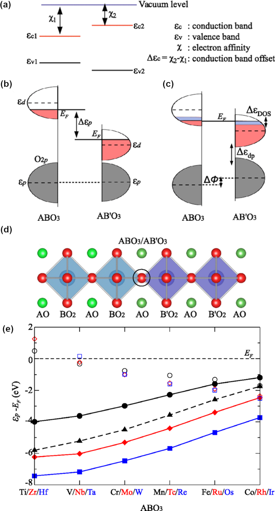
Density functional theory (DFT) is one of the most widely used theoretical modeling techniques to predict the charge transfer mechanism in the metal oxides interface. Different metal oxides interfaces follow different charge transfer mechanisms. Particularly in Mott–Hubbard insulators, the O 2p band alignment and the competition between crystal field and correlation energy of d electrons are crucial to determine the electronic rearrangement [Reference Zhong and Hansmann104]. Generally, the apical oxygen atom at the interface [see Fig. 11(d)] is shared by the materials at the heterostructure interface. This results in the alignment of O 2p bands at the interface. However, considering the O 2p band alignment alone disregards the creation of the internal electric field that balances the electrochemical potential between two B-sites and prevents further charge transfer. Hence, interfacial charge transfer between two materials transfer cannot completely be understood relying only on O 2p band alignment. An extra factor that comes into play is the rearrangement of the d- bands on B-site cations. Specifically, the density of states of B-site cations of each material reflects a clear picture of possible electronic rearrangement.
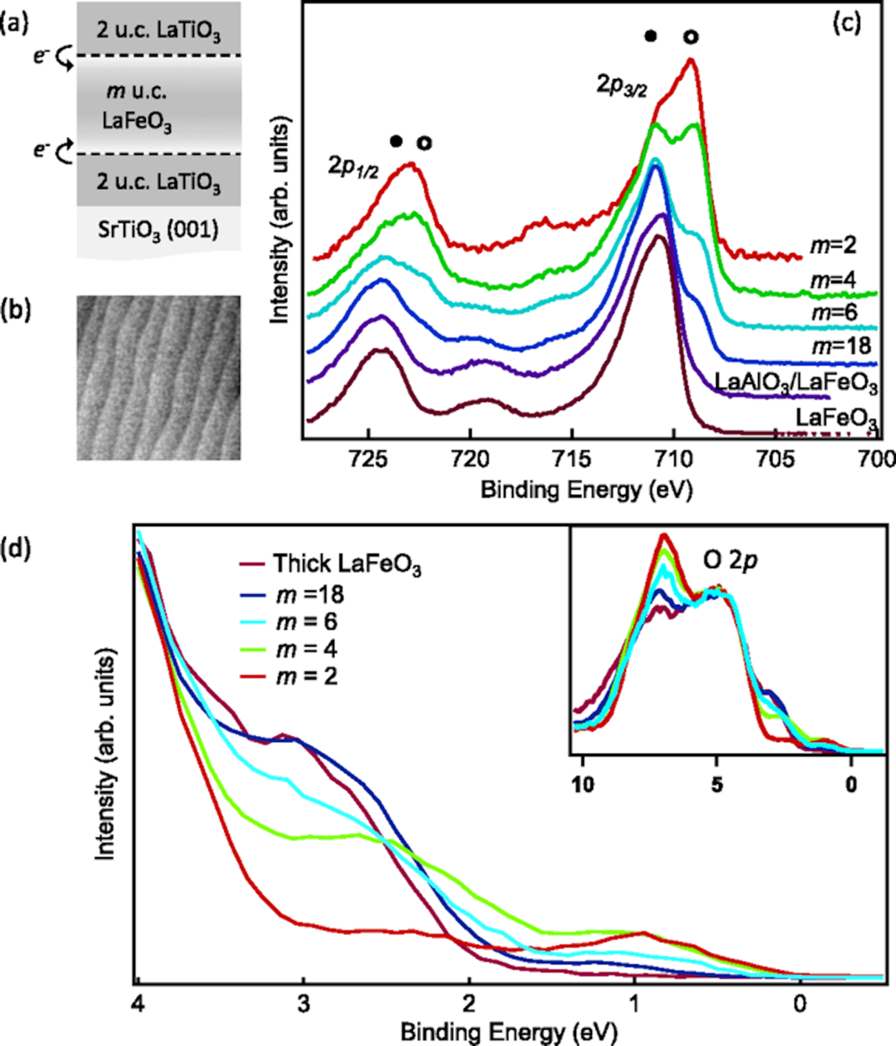
As an example, the Ti atom would be expected to donate electrons to the Fe atom at the LaTiO3/LaFeO3 interface, implying a formal charge of 4+ for the interfacial Ti ion and the shifting of Fe from a 3+ state to a 2+ state near the interface [Reference Zhong and Hansmann104]. A theoretical prediction of charge transfer in the metal oxides interface is supported by XPS analysis both qualitatively and quantitatively to resolve the valence band structure. XPS is well known for its high sensitivity to the variations in valence states of transition metal ions. Kleibuker et al. [Reference Kleibeuker, Zhong, Nishikawa, Gabel, Müller, Pfaff, Sing, Held, Claessen, Koster and Rijnders110] showed an extra peak at ~2 eV lower binding energy is observed for the LaFeO3/LaTiO3 heterointerface in reference to the bulk LaFeO3 for Fe 2p XPS spectra, as shown in Fig. 12. This extra peak in Fig. 12(c) at slightly lower binding energy, denoted by an open circle, represents the presence of the Fe2+ state along with the typical Fe3+ state at higher binding energy, denoted by a solid circle. Interestingly, the extra peak gets more pronounced with the decrease in thickness of the LaFeO3 layer which indicates that the charge transfer occurs near or at the interface. To understand the rearrangement mechanism for transfer of charge, a valence band spectrum in XPS is analyzed experimentally. The evolution of an extra peak around 1 eV in valence band spectra represents the completely filled t 2g band of Fe2+ in a low-spin configuration. Separate measurements of the Ti 2p spectrum confirmed 4+ formal charge of Ti, indicative of charge transfer from Ti to Fe of 1 e−/UC at the interface.
(a) Sketch of the LaTiO3/LaFeO3 sample geometry. (b) A typical 1 × 1 μm AFM height image of a LaTiO3/LaFeO3 heterostructure. (c) Fe 2p XPS spectra of LaTiO3/LaFeO3 heterostructures for various thicknesses of LaFeO3, as well as of a 30 u.c. LaFeO3 film and a (2/2) LaAlO3/LaFeO3 heterostructure. The solid and open circles mark the Fe3+ and Fe2+ peaks, respectively. (d) Valence band XPS spectra of LaTiO3/LaFeO3 heterostructures for various thicknesses of LaFeO3. All spectra were taken near normal emission (θ = 3°). Reprinted figure with permission from J.E. Kleibeuker et al. [Reference Kleibeuker, Zhong, Nishikawa, Gabel, Müller, Pfaff, Sing, Held, Claessen, Koster and Rijnders110]. Copyright 2014 by the American Physical Society.
For other instances, the preparation of complex superlattices that are different from regular heterojunctions helps to enlighten the process of charge transfer. One such example is charge transfer in LaTiO3/LaNiO3/LaAlO3 heterostructures [Reference Disa, Kumah, Malashevich, Chen, Arena, Specht, Ismail-Beigi, Walker and Ahn5]. In the bulk structure, B-site cations of each material have 3+ oxidation states. However, because the d 0 Ti4+ is the more stable oxidation state, one electron can move from the Ti t 2g band to Ni e g band resulting in Ni transitioning to a 2+ state from a 3+ state that is also more energetically favorable [Reference Disa, Kumah, Malashevich, Chen, Arena, Specht, Ismail-Beigi, Walker and Ahn5]. Interestingly, XAS confirmed this charge transfer and showed a preferential orbital occupation of the Ni 3d z2 e g orbital, producing the orbital occupation that makes LaNiO3 resemble the superconducting cuprates. This type of approach to interface-engineered symmetry breaking is an alternative approach to the reduced (Nd,Sr)NiO2 films that have recently demonstrated superconductivity [Reference Li, Lee, Wang, Osada, Crossley, Lee, Cui, Hikita and Hwang56]. Similar measurements for a LaNiO3/LaMnO3 heterostructure indicated electron transfer from Mn to Ni at the interface [Reference Hoffman, Tung, Nelson-Cheeseman, Liu, Freeland and Bhattacharya4]. A combined XPS and XAS study of LaCoO3/LaTiO3 heterostructures also indicated charge transfer to produce Co2+ and Ti4+ valences at the interface [Reference Araizi-Kanoutas, Geessinck, Gauquelin, Smit, Verbeek, Mishra, Bencok, Schlueter, Lee, Krishnan, Fatermans, Verbeeck, Rijnders, Koster and Golden111]. Charge transfer in SrMnO3/SrIrO3 to produce Mn3+ and Ir5+ [Reference Nichols, Gao, Lee, Meyer, Freeland, Lauter, Yi, Liu, Haskel, Petrie, Guo, Herklotz, Lee, Ward, Eres, Fitzsimmons and Lee46, Reference Okamoto, Nichols, Sohn, Kim, Noh and Lee47] and LaMnO3/SrIrO3 to produce Mn2+ and Ir5+ [Reference Suraj, Omar, Jani, Juvaid, Hooda, Chaudhuri, Rusydi, Sethupathi, Venkatesan, Ariando and Rao48] heterostructures has also been demonstrated. Each of these examples agrees with the model put forward by Zhong and Hansmann [Reference Zhong and Hansmann104], indicating the value of their approach in predicting interfacial charge transfer and band alignment based on initially aligning the O 2p energy bands. Future studies are likely to benefit from moving beyond 3d transition metal systems into the 4d and 5d blocks of the periodic table to generate novel interfacial phenomena.
Experimental design considerations
We have shown above several examples of the use of in situ XPS studies to probe interfacial phenomena in oxide heterostructures. The availability of an XPS appended to a growth chamber makes these studies very convenient and generates important physical insights as soon as the synthesis is complete. However, the knowledge gleaned from such studies is constrained by both the physical limitations of XPS and by the researcher's chosen design for the synthesized heterostructure. We have already discussed the information depth within the sample for an Al Kα source, which is limited to ~5 nm for photoemission normal to the film surface. Thus, band alignment and charge transfer studies are impractical for interfaces that are more than 5 nm below the surface.
One must also consider which interfaces in a multilayer will exhibit emergent properties, the chemical stability of the surface in vacuum and in atmosphere, and potential interference due to overlapping core-level peak energies. In the latter case, LaNiO3 is a good example of a material that cannot be easily examined via XPS due to the overlap of the La 3d 3/2 and the Ni 2p 3/2. The LaNiO3/LaTiO3 charge transfer described above would be very difficult to study in XPS, though the use of the Ni 3p peak does provide one way to probe changes in Ni valence [Reference Qiao and Bi112]. Furthermore, the depth sensitivity of XPS means that if two interfaces are present in a multilayer, as in the case of the LaTiO3/LaFeO3/LaTiO3 trilayer in Fig. 12(a), then the top interface will generate a majority of the signal and any phenomena at the bottom interface may be difficult or impossible to measure. Finally, while in situ measurements protect against changes due to atmospheric exposure, some surfaces may be modified even during the sample cooldown process [Reference Aeschlimann, Preziosi, Scheiderer, Sing, Valencia, Santamaria, Luo, Ryll, Radu, Claessen, Piamonteze and Bibes32] or will have intrinsic oxygen vacancies [Reference Golalikhani, Lei, Chandrasena, Kasaei, Park, Bai, Orgiani, Ciston, Sterbinsky, Arena, Shafer, Arenholz, Davidson, Millis, Gray and Xi55]. The deposition of a protective capping layer during the growth process that will not induce any chemical changes in the underlying materials is thus valuable even for in situ studies if a surface is unstable.
Future directions for in situ and related studies
Hard X-ray photoelectron spectroscopy
Advances in spectroscopy over the past decade have largely been driven by the development of new techniques from synchrotron light sources. These have included the emergence of hard X-ray photoelectron spectroscopy (HAXPES). A variety of new HAXPES beamlines [Reference Reininger, Woicik, Hulbert and Fischer113, Reference Rueff, Rault, Ablett, Utsumi and Céolin114, Reference Schlueter, Gloskovskii, Ederer, Schostak, Piec, Sarkar, Matveyev, Lömker, Sing, Claessen, Wiemann, Schneider, Medjanik, Schönhense, Amann, Nilsson and Drube115, Reference Yasuno, Oji, Koganezawa and Watanabe116] have been constructed as new light sources are brought online, enabling XPS studies that are not limited by the surface sensitivity of lab sources. Performing XPS studies with X-ray photon energies >2 keV provides more bulk sensitivity and enables access to transition metal 1s core levels that cannot be examined in a conventional Al Kα laboratory source. As discussed previously, the IMFP for photoelectrons, λ, scales with the square root of electron kinetic energy for high kinetic energies. This means that electrons with kinetic energies ~10 keV will have IMFP approaching 10 nm. An IMFP of 10 nm produces depth sensitivities such that only half of the escaping photoelectrons will be from the top 6.5 nm of the sample and only 10% of the signal comes from the surface (top 1.0 nm). Conversely, for an IMFP of 1.5 nm that would be typical for a lab source, half of the signal is generated from the top 1.0 nm and only 3% of the signal comes from 5.0 nm below the surface. Thus, HAXPES measurements enable studies of deeply buried interfaces more than 5 nm below the film surface that would be impossible with a lab source. Numerous synchrotron studies have made great use of HAXPES to probe oxide interfaces, including the LaAlO3/SrTiO3 interface [Reference Sing, Berner, Goß, Müller, Ruff, Wetscherek, Thiel, Mannhart, Pauli, Schneider, Willmott, Gorgoi, Schäfers and Claessen91, Reference Gabel, Zapf, Scheiderer, Schütz, Dudy, Stübinger, Schlueter, Lee, Sing and Claessen117] and the LaNiO3 surface [Reference Gray, Janotti, Son, LeBeau, Ueda, Yamashita, Kobayashi, Kaiser, Sutarto, Wadati, Sawatzky, Van de Walle, Stemmer and Fadley53] that we have already discussed. We refer the reader to several good reviews and examples of HAXPES studies, [Reference Fadley and Nemšák118, Reference Chambers and Woicik119, Reference Sing, Claessen, Cancellieri and Strocov120, Reference Gariglio, Cancellieri, Cancellieri and Strocov121] and will focus our attention in this section on the use of the technique to probe BaSnO3.
BaSnO3 is an exciting wide band gap oxide that has been shown to exhibit extremely high electron mobilities at room temperature (150–200 cm2/V-s) when grown by molecular beam epitaxy [Reference Paik, Chen, Lochocki, Seidner H, Verma, Tanen, Park, Uchida, Shang, Zhou, Brützam, Uecker, Liu, Jena, Shen, Muller and Schlom122, Reference Prakash, Xu, Faghaninia, Shukla, Ager Iii, Lo and Jalan123, Reference Raghavan, Schumann, Kim, Zhang, Cain and Stemmer124]. Unlike other perovskite oxides, the conduction band of BaSnO3 is derived from Sn 5s orbitals, [Reference Sallis, Scanlon, Chae, Quackenbush, Fischer, Woicik, Guo, Cheong and Piper125, Reference Lebens-Higgins, Scanlon, Paik, Sallis, Nie, Uchida, Quackenbush, Wahila, Sterbinsky, Arena, Woicik, Schlom and Piper126] which enable a much greater degree of electronic dispersion and carrier mobility than, i.e., 3d orbitals in SrTiO3. While this dramatic enhancement of mobility is of great benefit for potential future device applications, such as field-effect transistors [Reference Park, Kim, Ju, Park, Kim and Char127, Reference Park, Paik, Nomoto, Lee, Park, Grisafe, Wang, Salahuddin, Datta, Kim, Jena, Xing and Schlom128, Reference Krishnaswamy, Bjaalie, Himmetoglu, Janotti, Gordon and Van de Walle129], it also poses challenges to effective doping, both through the use of n-type donors [Reference Weston, Bjaalie, Krishnaswamy and Van de Walle130] and across interfaces through modulation doping and charge transfer [Reference Chambers, Kaspar, Prakash, Haugstad and Jalan103]. HAXPES has been particularly useful to elucidate the nature of the electronic transport in BaSnO3 and in examining interfacial carrier profiles in stannate heterostructures.
Initial studies of La-doped BaSnO3 via HAXPES focused on understanding the nature of the conduction band profile in the material, by probing electronic states near the Fermi level [Reference Sallis, Scanlon, Chae, Quackenbush, Fischer, Woicik, Guo, Cheong and Piper125, Reference Lebens-Higgins, Scanlon, Paik, Sallis, Nie, Uchida, Quackenbush, Wahila, Sterbinsky, Arena, Woicik, Schlom and Piper126]. Through ex situ synchrotron HAXPES studies with 4 keV photon energy, the first evidence of mobile Sn 5s electrons near the Fermi level was reported [Reference Sallis, Scanlon, Chae, Quackenbush, Fischer, Woicik, Guo, Cheong and Piper125]. Laboratory-source Al Kα studies of the same samples could not confirm the presence of carriers at the Fermi edge. The authors attributed this observation to the greater photoelectron cross section for Sn 5s with 4 keV photons in comparison to the 1487 eV lab source. However, given continued studies of the stability of dopants in BaSnO3 [Reference Weston, Bjaalie, Krishnaswamy and Van de Walle130], it also seems possible that atmospheric exposure led to the depletion of the surface carriers, which would explain the absence of observed carriers in the lab-source experiments. Carriers in identically doped BaSnO3 were later observed in a lab-source experiment [Reference Zhang, Han, Luo, Xiang, Zou, Oropeza, Gu and Zhang131], lending further credence to this possibility. It is also possible that the HAXPES experiments [Reference Sallis, Scanlon, Chae, Quackenbush, Fischer, Woicik, Guo, Cheong and Piper125] were successful due to the greater probe depth for hard X-rays, which overcomes the surface depletion. This explanation would provide another example of the effects of atmospheric exposure on metastable electronic states near the Fermi level. Further HAXPES studies of BaSnO3 doped with differing La concentrations helped to explain the nature of the conduction band filling and band gap renormalization due to the Burstein–Moss effect [Reference Lebens-Higgins, Scanlon, Paik, Sallis, Nie, Uchida, Quackenbush, Wahila, Sterbinsky, Arena, Woicik, Schlom and Piper126]. These studies have paved the way for the development of stannate thin films and heterostructures, as research moves from understanding the nature of electronic conduction to confinement of carriers in a high-mobility 2DEG for device applications.
Modulation doping of BaSnO3 through engineering of band alignment and charge transfer is a key requirement for a 2DEG structure. Impurity scattering from La donor ions is a key limitation to the further enhancements of mobility in electron-doped BaSnO3 [Reference Prakash, Xu, Faghaninia, Shukla, Ager Iii, Lo and Jalan123]. To overcome this, engineering of a heterostructure with conduction band electrons at greater energies than the BaSnO3 conduction band is necessary. In one such heterostructure, a 14 nm La-doped SrSnO3 top layer was engineered such that free carriers in that layer could flow “downhill” to an undoped BaSnO3 below the SrSnO3 layer to form a 2DEG [Reference Prakash, Quackenbush, Yun, Held, Wang, Truttmann, Ablett, Weiland, Lee, Woicik, Mkhoyan and Jalan132]. Given the thickness of the SrSnO3 top layer, synchrotron HAXPES studies were needed to probe the buried interface. Using a photon energy of 5.93 keV, the group was able to extract the interfacial band alignment and estimate the degree of charge transfer into the underlying BaSnO3. These results are shown in Fig. 13. Interestingly, the extracted band profile in Fig. 13(d) could be explained by surface carrier depletion from atmospheric exposure, as discussed above regarding La-doped BaSnO3 [Reference Sallis, Scanlon, Chae, Quackenbush, Fischer, Woicik, Guo, Cheong and Piper125]. These results show that the band alignment techniques that have been used for in situ studies for many years can be applied to more challenging structures using hard X-ray sources that probe more deeply into materials. Continued development of HAXPES will dramatically improve the ability to measure interfacial phenomena in heterostructures that are not limited to a few nm in thickness due to the lab-based X-ray energies.
Band alignment at La-doped SrSnO3 (LSSO)/SrSnO3(SSO)/BaSnO3 (BSO) interface. (a) VB spectra of the reference BSO (green) (56 nm BSO/SrTiO3 (001)) and LSSO (blue) (41 nm LSSO/8 nm SSO/GdScO3 (110)) films. Electronic states near the Fermi states are magnified. Inset shows the La 3d 5/2 core-level X-ray photoelectron spectra, (b) VB spectra of the SSO/BSO heterostructure (red) along with the fit (black) using linear combination of the reference VB spectra (dotted green and blue lines) to determine the VB offset. (c) An energy level flat-band diagram showing the measured band offsets between LSSO and BSO, and (d) conduction band minima (red) referenced to the Fermi level (top panel) and 3D carrier density, n 3D (blue) as a function of depth for the SSO/BSO (bottom panel). The shaded regions indicate 2D density in LSSO and BSO layers after the charge transfer. Reprinted with permission from A. Prakash et al. [Reference Prakash, Quackenbush, Yun, Held, Wang, Truttmann, Ablett, Weiland, Lee, Woicik, Mkhoyan and Jalan132]. Copyright 2019 American Chemical Society.
Standing-wave XPS
While HAXPES measurements are one approach to probe more deeply within a material and examine both bulk electronic structure and buried interfaces, the underlying physics of the photoemission process is unchanged. As we showed above, HAXPES measurements can still be affected by surface chemistry of the films. The standing-wave XPS (SW-XPS) approach has emerged over the past decade, specifically focusing on studies of superlattice structures that exhibit regularly repeating interfaces. By varying the incoming X-ray angle such that the Bragg diffraction condition is satisfied for the superlattice, the intensity of the electric field is modulated across the interface. A stronger Bragg reflection produces a greater standing-wave intensity and greater modulation of the electric field strength across the repeating superlattice formula unit. The physics of SW-XPS has been described in more detail in various references [Reference Fadley and Nemšák118, Reference Gray133, Reference Gray, Nemšák and Fadley134, Reference Nemšák, Gray, Fadley, Cancellieri and Strocov135]. Here, we aim to discuss the applications of SW-XPS to understanding interfacial phenomena and present opportunities to expand on this unique approach by designing interfacial materials that will be well suited for SW-XPS studies.
As an initial example, we present a study of layer-resolved band alignment in a superlattice achieved through careful design of a superlattice structure. The structure and electric field strength modulation is shown schematically in Fig. 14 for a study of a LaCrO3–SrTiO3 superlattice using ~830 eV photon energy near the La M 5 resonance. [Reference Lin, Kuo, Comes, Rault, Rueff, Nemšák, Taleb, Kortright, Meyer-Ilse, Gullikson, Sushko, Spurgeon, Gehlmann, Bowden, Plucinski, Chambers and Fadley136] In this case, the formula of 10 UCs of SrTiO3 followed by 5 UCs of LaCrO3 over 10 repeating layers in the superlattice was chosen to maximize the Bragg reflection and thus the sensitivity to individual interfaces. By choosing the superlattice periodicity prior to growth and considering the subsequent SW-XPS experiment, the largest standing-wave response ever achieved was reported, with individual core-level intensities varying by ~50% as the X-ray angle was varied across the Bragg peak. This enabled the extraction of the band alignment across the entire 15-unit-cell structure through careful modeling of the core-level peak positions as a function of incoming angle, producing good agreement with DFT models [Reference Lin, Kuo, Comes, Rault, Rueff, Nemšák, Taleb, Kortright, Meyer-Ilse, Gullikson, Sushko, Spurgeon, Gehlmann, Bowden, Plucinski, Chambers and Fadley136, Reference Comes, Spurgeon, Heald, Kepaptsoglou, Jones, Ong, Bowden, Ramasse, Sushko and Chambers137].
(a) Schematic of the superlattice made up of 10 bilayers of LCO and STO, consisting of 5 UCs of LCO, 17.6 Å thick, and 10 UCs of STO, 39.2 Å thick, grown epitaxially on a Nb-doped STO(001) substrate. The two sources of the standing-wave structure in the rocking curves are indicated: Bragg reflection from the multilayer with period d ML and Kiessig fringes associated with the full thickness of the multilayer stack D ML. Experimental (open circles) and simulated (solid) rocking curves of representative elemental states at photon energies of (b) 829.7 eV and (c) 831.5 eV. The colored dash lines are the guides to the eye to indicate the phase of the rocking curves in (b and c) to show sensitivity to the interfacial termination (SrO/CrO2 versus TiO2/LaO). The electric field strength distribution derived from X-ray optics calculations at two energies near the La M5 resonance, (d) 829.7 eV and (e) 831.5 eV as a function of sample depth and incidence angle. Note the significant shift in position between the two energies. The corresponding photoemission yields, (f and g), plotted on log10 scales. Adapted figure with permission from S.-C. Lin et al. [Reference Lin, Kuo, Comes, Rault, Rueff, Nemšák, Taleb, Kortright, Meyer-Ilse, Gullikson, Sushko, Spurgeon, Gehlmann, Bowden, Plucinski, Chambers and Fadley136] . Copyright 2018 by the American Physical Society.
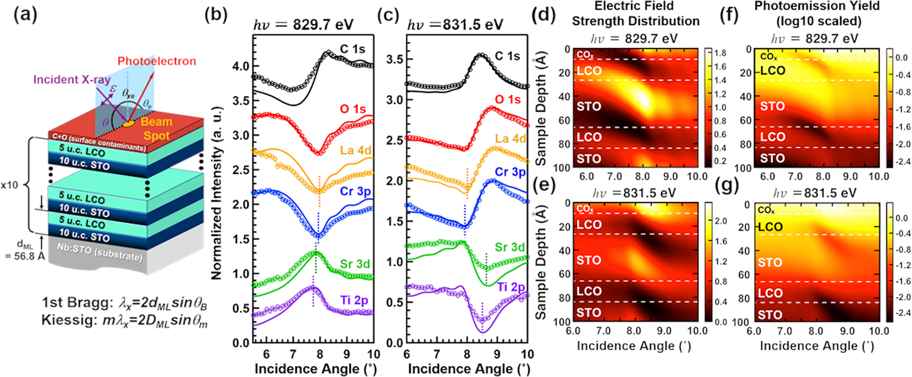
The SW-XPS technique has been used to probe changes in interfacial chemistry in a variety of other superlattice systems. Evidence for Ni2+ valence near the interface with SrTiO3 in 4 u.c. LaNiO3–4 u.c. SrTiO3 superlattices was reported [Reference Kaiser, Gray, Conti, Son, Greer, Perona, Rattanachata, Saw, Bostwick, Yang, Yang, Gullikson, Kortright, Stemmer and Fadley138]. Studies of LaNiO3–CaMnO3 superlattices showed similar effects, with Ni2+ states observed at the interface [Reference Chandrasena, Flint, Yang, Arab, Nemšák, Gehlmann, Özdöl, Bisti, Wijesekara, Meyer-Ilse, Gullikson, Arenholz, Ciston, Schneider, Strocov, Suzuki and Gray139]. Likewise, changes in the interfacial Mn valence in (La,Sr)MnO3–SrTiO3 superlattices were also observed [Reference Gray, Papp, Balke, Yang, Huijben, Rotenberg, Bostwick, Ueda, Yamashita, Kobayashi, Gullikson, Kortright, de Groot, Rijnders, Blank, Ramesh and Fadley140]. Collectively, these studies have shown that the technique provides additional sensitivity to changing interfacial chemical states at interfaces. The X-ray standing wave provides a novel way to isolate the interfacial contribution to the detected signal that goes beyond conventional angle-resolved XPS. However, the design of the superlattice and choice of materials system under examination plays a significant role in how much information can be extracted from the measurement. For example, superlattices with large differences in density between layers produce larger superlattice Bragg peaks, so that a superlattice comprised of, i.e., SrTiO3 and LaTiO3 layers will produce a greater peak than one comprised of, i.e., SrTiO3 and SrVO3 or LaTiO3 and LaVO3 layers. This means that the technique is currently only suitable for select combinations of materials.
Ideally, SW-XPS could be used to measure not simply changes in interfacial chemistry but also to probe emergent interfacial electronic states near the Fermi level. There have also been some efforts to employ SW-XPS to generate ARPES information as a function of depth within the material, including studies of SrTiO3–GdTiO3 [Reference Nemšák, Conti, Gray, Palsson, Conlon, Eiteneer, Keqi, Rattanachata, Saw, Bostwick, Moreschini, Rotenberg, Strocov, Kobayashi, Schmitt, Stolte, Ueda, Kobayashi, Gloskovskii, Drube, Jackson, Moetakef, Janotti, Bjaalie, Himmetoglu, Van de Walle, Borek, Minar, Braun, Ebert, Plucinski, Kortright, Schneider, Balents, de Groot, Stemmer and Fadley141] and SrTiO3–(La,Sr)MnO3 [Reference Gray, Minár, Plucinski, Huijben, Bostwick, Rotenberg, Yang, Braun, Winkelmann, Conti, Eiteneer, Rattanachata, Greer, Ciston, Ophus, Rijnders, Blank, Doennig, Pentcheva, Kortright, Schneider, Ebert and Fadley142] superlattices. These results are promising demonstrations of the technique but provided limited insights into emergent interfacial physical phenomena due in large part to the relatively weak X-ray standing wave. The weakness of the standing-wave can be observed in small variation of the core-level peak intensities as a function of angle (~20–30%). This means that differences in the ARPES data as a function of angle are fairly small and it is difficult to extract clear information about the electronic structure in individual layers of the superlattice or at a particular interface. In most cases of SW-XPS studies to date, the challenge has not been the technique but the limitation of the samples themselves. We suggest that a somewhat different model could bear fruit.
Because the photon energies for most SW-XPS studies have been in the soft X-ray regime where it is possible to take advantage of elemental resonances to enhance reflectivity, the measurements are still limited to the top few nm of the sample. Thus, the underlying superlattice serves only to generate the X-ray standing wave that modulates the field strength across the topmost repeat layer of the sample and does not have a meaningful effect on the actual data being measured. It, therefore, makes sense to choose an underlying superlattice solely from the perspective of generating the strongest standing-wave intensity while not confusing the data interpretation from the relevant interface in other ways. In this sense, the superlattice serves as a novel substrate for the actual experimental interface, as has been applied in other cases for non-epitaxial films such as the Fe–MgO interface [Reference Döring, Schönbohm, Berges, Schreiber, Bürgler, Schneider, Gorgoi, Schäfers, Papp, Balke, Fadley and Westphal143] and ambient-pressure XPS measurements on Fe2O3 [Reference Nemšák, Shavorskiy, Karslioglu, Zegkinoglou, Rattanachata, Conlon, Keqi, Greene, Burks, Salmassi, Gullikson, Yang, Liu, Bluhm and Fadley144]. For example, a SrTiO3–BaTiO3 superlattice is relatively easy to synthesize and would provide strong standing-wave effects across the Ba M 5 resonance (~780 eV). Predictions of superlattice Bragg peaks for various BTOn–STOn superlattice structures using the X-ray Interactions with Matter website [Reference Gullikson145, Reference Henke, Gullikson and Davis146] provided by the Center for X-ray Optics at Lawrence Berkeley National Laboratory are shown in Fig. 15(a). The electric field strength varies as the square root of reflectivity, meaning that values greater than 0.1 on the scale (dotted line) will produce modulations of XPS peak intensity of 30% or better. The superlattices could then be used as X-ray mirror substrates for any number of intriguing interfacial materials to produce much stronger standing-wave effects. A schematic of such a heterostructure is shown in Fig. 15(b), with a BTO5–STO5 superlattice with an arbitrary SrMO3-SrM'O3 interface highlighted in yellow that will be strongly probed by the standing wave from the underlying mirror. Given this opportunity to shift the approach to standing-wave measurements, groups should consider the SW-XPS experiment when designing both their superlattice mirror layer and the interface of interest. Others have proposed additional approaches to enhance standing-wave effects in these measurements [Reference Gray133]. Ideally, collaborations between synthesis groups and experts in SW-XPS early in the research process will produce samples that are particularly well suited to answer specific questions about the properties of an interface.
(a) Modeled X-ray reflectivity for three n-unit cell BaTiO3 (BTOn)/n-unit cell SrTiO3 (STOn) superlattices on SrTiO3 substrates at the Ba M5 energy resonance; (b) Schematic of BTO5–STO5 superlattice mirror to probe an arbitrary SrBO3-SrB'O3 interface (highlighted in yellow).
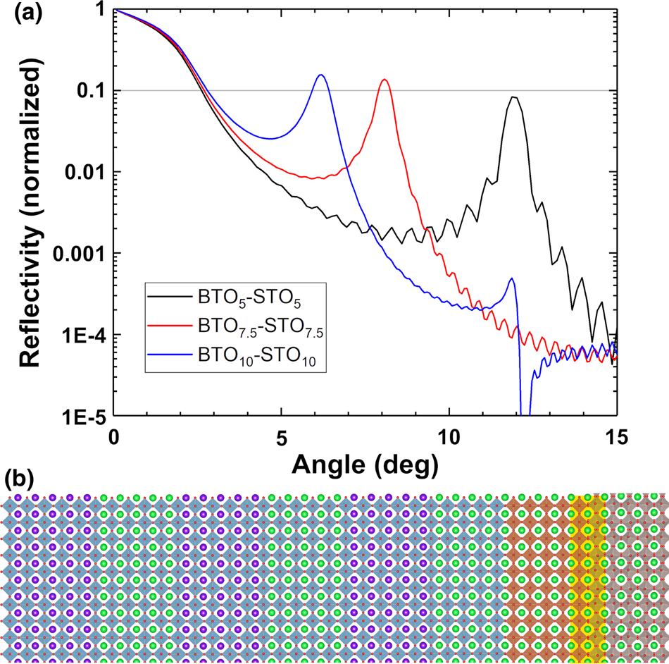
Future applications
In summary, synchrotron XPS techniques have generated significant new insights into buried oxide interfaces by taking advantage of the variable X-ray energies that are provided from a synchrotron source that cannot be replicated in a lab. Many of these approaches have only been pursued over the past decade, however, leaving significant opportunities to refine the practices to better extract novel physics from the experiments. For example, many beamlines have begun to integrate MBE or PLD growth systems in situ as has been done in a lab environment for many years [Reference Palomino, Stavitski, Waluyo, Chen-Wiegart, Abeykoon, Sadowski, Rodriguez, Frenkel and Senanayake147, Reference Eres, Rouleau, Lu, Zhang, Benda, Lee, Tischler and Fong148]. We have shown in this review that surface exposure must be considered when interpreting results, even for HAXPES studies. It thus makes sense to perform SW-XPS and HAXPES studies using in situ growth capabilities at the beamline whenever possible. Alternatively, the use of a vacuum suitcase to transport samples from a home synthesis laboratory to the user facility can enable synchrotron studies that replicate in situ conditions.
Another promising new opportunity has been enabled by the development of lab-based HAXPES instruments [Reference Regoutz, Mascheck, Wiell, Eriksson, Liljenberg, Tetzner, Williamson, Scanlon and Palmgren149]. Rather than traditional Al or Mg sources, these commercially available instruments employ a 3d transition metal or metalloid such as Cr or Ga to produce monochromatic Kα photons with energies greater than 5 keV. The recent development of a liquid-metal Ga source with a Rowland circle monochromator has produced fluxes that are within a factor of 200 of synchrotron sources, making it possible to perform measurements in reasonable times in a lab environment [Reference Regoutz, Mascheck, Wiell, Eriksson, Liljenberg, Tetzner, Williamson, Scanlon and Palmgren149]. To date, we know of no laboratory that has an oxide or other complex materials film growth chamber attached in situ to a HAXPES instrument, but this would be an excellent resource for future film synthesis user facilities. An instrument suite integrating film synthesis and the large probing depth of a hard X-ray source in situ would be an invaluable resource for studies of charge transfer and band alignment in future complex heterostructures like the one presented in Fig. 13 [Reference Prakash, Quackenbush, Yun, Held, Wang, Truttmann, Ablett, Weiland, Lee, Woicik, Mkhoyan and Jalan132].
Summary
In conclusion, we have examined the state-of-the-art in oxide thin films and interfaces by focusing on the synergy that is possible when epitaxial film synthesis and XPS are integrated in situ. We have shown how XPS can be used to improve the synthesis process to observe film contamination, stoichiometry, surface termination, and surface chemistry. These day-to-day measurements can be extremely valuable to film growers as they optimize the growth process. By demonstrating the effects that metastable surfaces and atmospheric exposure can have on measured film properties, we show both the benefit of performing such measurements in situ. In general, energetically unfavorable states will not be preserved at a film surface. These include the reduction of Ni3+ to Ni2+ and the oxidation of Ti3+ to Ti4+ and Sn3+ to Sn4+ upon atmospheric exposure. A corollary to these effects is the care that must be taken in interpreting other spectroscopy results as well as other measurements such as electronic transport.
We have also shown how more complex XPS experiments can be designed to measure interfacial intermixing, valence band offsets, and charge transfer. By examining several case studies, we showed the importance of designing thin film heterostructures with the subsequent XPS experiment in mind. Predictive models for band alignment and interfacial charge transfer based on the alignment of the O 2p bands can be valuable in selecting interfaces that are likely to generate novel properties, which are then readily measured via in situ XPS. Finally, we presented future directions for XPS-based studies of oxide interfaces that leverage advances in synchrotron and lab-based technologies to achieve high impact results. Bridging the gap between synthesis and characterization in these future studies will hopefully provide the oxide thin film community with a better understanding of the complex chemical and physical phenomena that drive emergent behavior in oxide heterostructures.
Acknowledgments
We thank Shalinee Chikara for assistance with the LaCoO3 deposition and XPS data acquisition shown in the paper. The authors gratefully acknowledge support from the Air Force Office of Scientific Research under award number FA9550-20-1-0034 and from the National Science Foundation Division of Materials Research under award number NSF-DMR-1809847. M.D.B. acknowledges fellowship support through the Alabama EPSCOR Graduate Research Scholars Program.


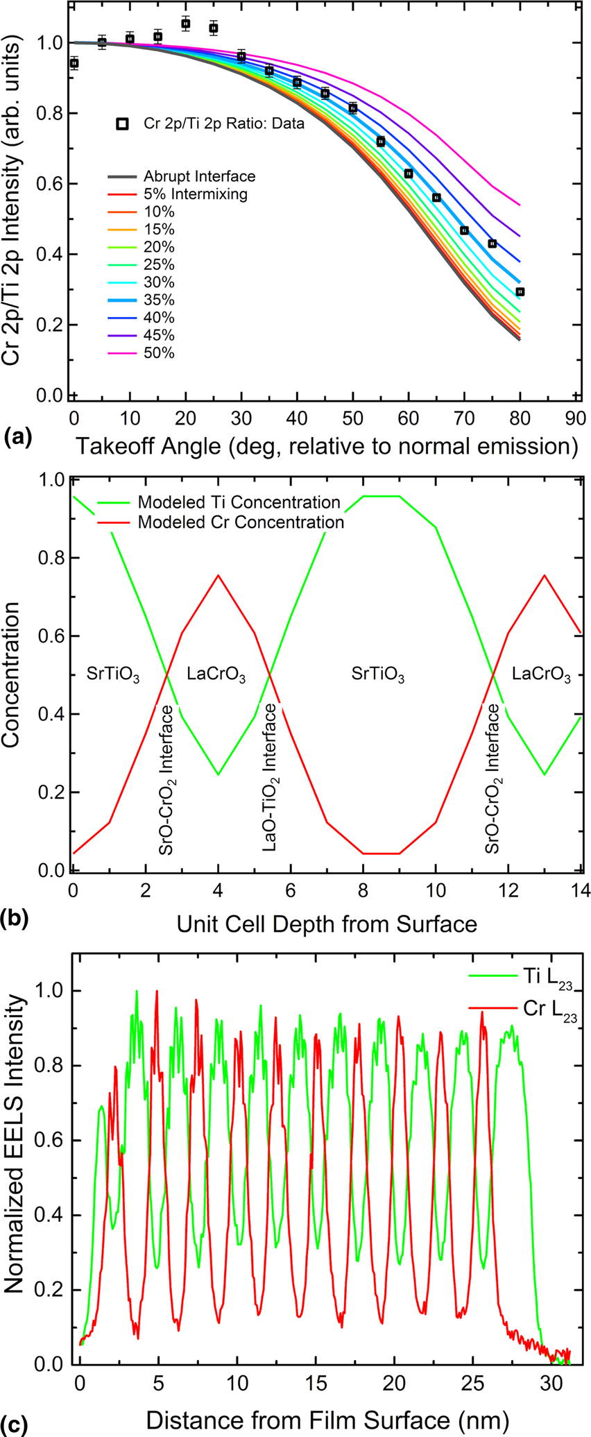


 Open access