





Introduction
The performance of wireless communications has to be continuously enhanced to satisfy the demand of more users and higher data rates. More elaborated standards, such as the 5th generation new-radio (5G NR) mobile communications utilize millimeter (mm)-wave frequencies, enabling wider bandwidths, higher-order modulations, and spatial-division multiple access in combination with multiple-input multiple-output (MIMO) capability [Reference Andrews, Buzzi, Choi, Hanly, Lozano, Soong and Zhang1]. Multi-beam systems were realized by flexible fully digital beamforming architectures [Reference Yang, Yu, Lan, Zhang, Zhou and Hong2, Reference Kim, Park, Kim, Minz and Park3], fixed-beam solutions based on Butler matrices [Reference Yang, Yang, Che, Fan and Xue4] or Rotman lenses [Reference Li, Chen, Sun, Zhao, Liu, Wu, Zhang, Lin, Sun, Zhao and Kang5]; and dual-beam variants [Reference Mondal, Singh and Paramesh6–Reference Sadhu, Tousi, Hallin, Sahl, Reynolds, Renström, Sjögren, Haapalahti, Mazor, Bokinge, Weibull, Bengtsson, Carlinger, Westesson, Thillberg, Rexberg, Yeck, Gu, Ferriss, Liu, Friedman and Valdes-Garcia8] were designed mainly for dual-polarized transmission for increased link capacity with polarization diversity as an MIMO variant. Various challenges arise at mm-wave frequencies [Reference Luo, Zaidi, Vihriälä, Giustiniano, Qi, Halbauer, Ktenas, Weiler, Miao and Lorca9]; circuit performance is affected by geometrical tolerances and dissipation losses, and the wireless transmission is attenuated by increased path loss and limited output power of the Tx amplifiers. Antenna arrays increase the equivalent isotropically radiated power (EIRP) levels, improve the link margins, and offer beamforming and steering capabilities [Reference Kibaroglu, Sayginer, Phelps and Rebeiz10]. The small footprints of these arrays and the system complexity require the application of dedicated highly integrated circuits, explicitly including multi-beam and polarization aspects [Reference Sadhu, Tousi, Hallin, Sahl, Reynolds, Renström, Sjögren, Haapalahti, Mazor, Bokinge, Weibull, Bengtsson, Carlinger, Westesson, Thillberg, Rexberg, Yeck, Gu, Ferriss, Liu, Friedman and Valdes-Garcia8]. The 64-element phased-array transceivers presented in [Reference Sadhu, Tousi, Hallin, Sahl, Reynolds, Renström, Sjögren, Haapalahti, Mazor, Bokinge, Weibull, Bengtsson, Carlinger, Westesson, Thillberg, Rexberg, Yeck, Gu, Ferriss, Liu, Friedman and Valdes-Garcia8, Reference Kibaroglu, Sayginer, Phelps and Rebeiz10] address base station applications. The limited resources of a user equipment (UE), e.g. battery size or mounting space, require complementary solutions with a significantly lower count of antenna elements [Reference Mondal, Singh and Paramesh6, Reference Dunworth, Homayoun, Ku, Ou, Chakraborty, Liu, Segoria, Lerdworatawee, Park, Park, Hedayati, Lu, Monat, Douglas and Aparin7, Reference Kim, Park, Song, Moon, Kim, Kim, Chang and Ho11].
The aforementioned system aspects were mapped onto a 30 GHz multi-beam polarization- and direction-agile analog front-end (FE) with an integrated 4 × 1 patch antenna array for a variable hardware-based evaluation. The term “analog front-end” reflects the implementation of the agility in real-time by entirely analog circuit functions, but hereinafter the more common notation front-end (FE) is used. To the best of the authors' knowledge, there is no public research to establish an integrated continuous electronic rotation of the linear polarization of a steerable antenna array. The random orientation of the UE devices and the multi-user scenarios require further studies for the Rx–Tx polarization alignment and exploitation of cross-polarization for interference mitigation. These investigations are established by the FE presented in this study. Although some primary findings and design problems regarding the analog part of the FE were previously reported [Reference Spira, Blau, Wagner, Schulz, Gutzeit, Müller, Thomä and Hein12, Reference Spira, Thomä and Hein13], we provide here a comprehensive description of the full operational system. Emphasis is laid on the FE system functions, followed by antenna design aspects and basic measurements, and finally radiation pattern and digital-signal over-the-air (OTA) measurements of the FE with the integrated antenna array. The entity of results not only provides a successful proof-of-principle, but also reveals limitations related to error vector magnitude (EVM) degradation.
System design
Figure 1 shows the main functional parts of the receiving FE module as a block diagram.
Block diagram of the mm-wave FE with two steerable beams (beam #1 and beam #2 fed by the upper and lower parts of the circuit, respectively) and controllable polarization (H- and V-polarizations created in the left-hand and right-hand parts of the circuit, respectively). The beamformers and down-converters of beam #1 are shown explicitly, whereas the control circuits for beam #2 are indicated in a simplified way.
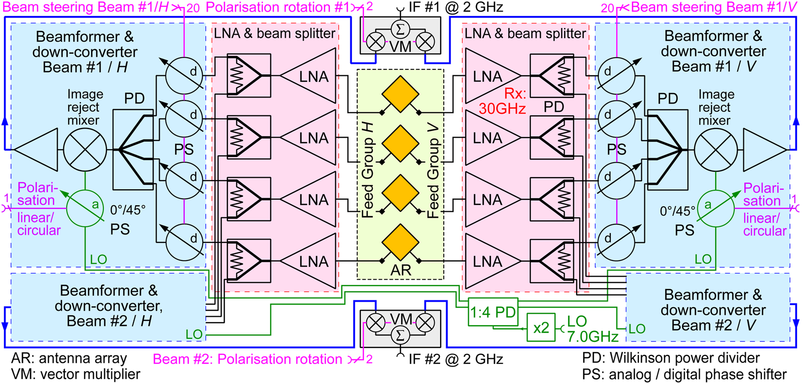
Low-noise amplifiers (LNA) decouple the dual-polarized antenna signals from the beam splitting power dividers. Phase shifters perform the beam steering, separately for each of the two orthogonal linear polarizations. The combined signals are down-converted by image reject mixers with internal local-oscillator (LO) frequency doubling, amplified, and summed with the orthogonally polarized component by a vector-multiplier integrated circuit. The weighted summation allows for an arbitrary rotation of the resulting polarization. The weights are set by DC voltages, because the multiplier is capable of handling baseband input signals. These functionalities are doubled and fed to a second beam, thus generating two separate agile beams. A common LO signal is frequency-doubled and power divided and supplied to all four mixers. All transmission paths are phase matched and allow an uncalibrated operation. The intermediate-frequency (IF) circuits and the integrated four-element patch antenna array currently limit the overall bandwidth to ~400 MHz, whereas the mm-wave block spans the entire frequency range from 28 to 31 GHz. Additional circuit boards deliver analog and digital control signals. The FE was assembled in the multi-layer low-temperature co-fired ceramics (LTCC) technology. Figure 2 displays a photograph of the assembled module, which consists of nine layers DuPont™ 9K7.
Photograph of the assembled FE with SMP plugs for RF connections, and a power supply and control connector. The module size measures 74 mm × 74 mm [Reference Spira, Blau, Thomä and Hein14].

Although previous study dealt with the comprehensive evaluation of the analog mm-wave transmission properties, this paper describes the results of recent OTA testing in a system context in greater detail, additionally addressing antenna design and measurements, because the antenna parameters determine to a large extent the performance of the overall system and thus the link-level parameters of broadband digitally modulated waveforms received with this FE, similar to realistic signals relevant for 5G mobile communications.
Antenna design
Originally, a 4 × 4 antenna array was envisaged. The active components required for such an array size, especially pre-amplifiers and active mixers, which necessarily have to be located near the antenna feed points, induce a dissipation power density exceeding the thermal limit; moreover, the available circuit area is insufficient in this case.
Since polarization agility should be ensured from the outset, in addition to beam steering, dual-polarized antenna elements have to be used. With 4 × 4 antenna elements, this means that the required LNAs, phase shifters, and mixers are doubled, so that high-power dissipation can be generated in a small area or volume. The resulting heat cannot be easily dissipated using conventional means like convection cooling using a heat sink. In addition, the size of the Green Tape Material DuPont™ 9K7 was limited to 75 mm × 75 mm of the processing area, which was a further restriction for the antenna design.
The basic idea of separately processing the linear H- and V-components of the polarization of the incident antenna signal is provided in Fig. 1. This also ensures polarization agility for elliptical polarization. In order to avoid the high thermal power density and taking the given area limitation into account, it was ultimately only possible to implement one antenna line consisting of four dual-polarized antenna elements in the design presented here.
Due to the decision to realize the demonstrator in LTCC technology and to operate it in the 28–31 GHz range, it was decided to adapt the antenna design to these conditions. In order to achieve a sufficiently broadband and dual-polarized antenna element with as little efforts as possible, and accounting for the technological LTCC limitations in terms of layer thickness and dimension tolerances, the choice fell on a square-shaped microstrip patch element, which basically can excite two orthogonal linear polarizations.
Due to the high permittivity of 9K7 (ɛr = 7.07), with a layer thicknesses of 0.315 mm (according to LTCC design rules), a correspondingly lower bandwidth of a microstrip patch must be expected if the excited field volume is completely filled with the ceramic material. For an estimation of the expected percentage bandwidth, equation (1) according to [Reference Kumar and Ray15] can be used:

where the parameter A takes different values depending on the effective electrical thickness heff = h/(λ 0 √ɛr) given in Table 1.
Parameter A versus the effective electrical thickness h eff introduced in relation to equation (1)

W and L denote the width and length of the patch element and h is the geometrical thickness. For a square patch, W = L = 1.8 mm and h = 0.315 mm with the design value ɛr = 7.07 and λ 0 = 10.17 mm (f = 29.5 GHz), we find A = 180 because the effective electrical thickness is about 0.0116. This means that the expected percentage bandwidth lies in the range of 2.1%. In relation to the center frequency, this corresponds to an absolute bandwidth of 620 MHz.
Attempts to reduce the effective dielectric permittivity of the substrate and thus increase the operational frequency bandwidth by creating an air cavity in the excited field volume were not pursued further due to additional technological challenges.
Further bandwidth limitations arise from the feeding topology. The individual antenna elements have to be excited with two orthogonal polarizations on two perpendicular sides. The inset feed technique avoids a bandwidth reducing line transformer, but numerical full-wave simulations result in a not feasible geometry.
The square patches were fed with λ/4-line transformers. Because of the necessity to feed the antenna ports through several layers of the 9K7 LTCC material, all potential discontinuities can be used as transformation elements, to avoid further bandwidth reductions, given that these can be suitably dimensioned through design optimization.
The multi-layer structure is depicted in Fig. 3(a) where the feed reaches from the upper plane of the patch antennas surrounded by the heat sink through the antenna ground, and then connects to a shielded stripline which is again fed to a microstrip transmission line.
Cross-section of the feedthroughs of the antenna signals of the multi-layer module mounted on a 2 mm copper heat sink, with microstrip and stripline structures on upper layers and the patch antenna array surrounded by the chamfered faces of the heat sink aperture (a) [Reference Spira, Blau, Wagner, Schulz, Gutzeit, Müller, Thomä and Hein12]. 3D view on the patch antennas with λ/4-transformers and vias for signal feed into the stripline plane (b).

It is important to note that the linear patch antenna array is actually located in a metal tub, which is formed by the antenna ground layer and the surrounding ground vias, see bottom part of Fig. 3. This design is intended to prevent any coupling of the antennas to the rest of the signal distribution network. The right-hand part of the linear array including the λ/4-microstrip line transformers and feedthroughs can be seen in detail in Fig. 4. This arrangement with the patches rotated by 45° avoids line elements between the patches and ensures that a spatially separate transmission of the orthogonal antenna signals becomes possible.
Top view of the right-hand side of the four-element dual-polarized microstrip antenna line. At the end of the λ/4-transformers, the feedthrough pads (0.25 mm in square) are clearly visible with vias in the center to the shielded stripline plane passing through the antenna ground-plane aperture (0.5 mm in square).

At the end of the λ/4-transformers, the feedthrough pads are placed together with the vias to the shielded stripline plane in their centers. This design was later integrated into the FE module, fabricated in the same LTCC technology with DuPont™ 9K7. Before integration, it was necessary to measure the return loss of each individual antenna port over the quite complex three-dimensional (3D) feed network so that there was the possibility to apply corrections as needed. In order to enable such measurements, the linear four-element array was manufactured on a separate 9K7 carrier of exactly the same layer stack as well as the antenna and feedthrough elements as the version to be integrated into the FE. The metallization around the antenna line was also identical to the design for the FE. The only difference was an additional extension of the microstrip lines to the mini-SMP plugs for characterizing the single patch antennas by vector network analysis. The fabricated LTCC carrier with the intended linear array is depicted in Fig. 5.
Left-hand panel: Top view of the separate 9K7 carrier with the four-element dual-polarized microstrip antenna line; right-hand panel: bottom view with the mini-SMP plugs with port numbers.

Antenna measurements
In a subsequent step, the reflection coefficients of the single-antenna ports were measured, in order to determine the resonant frequencies of the individual patches. The other ports were terminated with 50 Ω, and the mutual coupling was not recorded. The results are shown in Fig. 6 using the port numbers of Fig. 5. As it can be seen, the center frequencies of the four patches vary between 29.0 and 29.5 GHz, which additionally limits the usable bandwidth. The measured reflection coefficients include material and geometrical tolerances of the antenna patches, feed network, stripline-to-microstrip transition, and microstrip-to-miniSMP transition. Since the return loss was better than 20 dB at all ports, there was initially no need to modify the design of the line feeds. Alluding to Fig. 5, the geometrical differences between ports #1 and #8 and ports #4 and #5 with respect to the surrounding ground layout could be deduced approximately only.
Measured reflection coefficients of the orthogonal ports of the single patch antennas for center frequency comparison. Further details are provided in the main text.

In the last step before the integration of the antenna array into the FE, the radiation patterns of the single patches were measured in an anechoic shielded chamber. In order to emulate realistic circumstances, the antenna substrate was mounted on the intended heat sink.
The heat sink has a window slightly larger than the dimensions of the metal-free area around the four patches (31 mm × 10 mm) but with side bevels of 45° toward the antenna plane as depicted in Fig. 7. This measure should avoid the formation of a multi-mode waveguide with unfavorable effects on the radiation patterns and the polarization purity. In this context, it is to be noted that the thickness of the heat sink approaches a quarter of the free-space wavelength. From horn antennas it is well known that a large flare angle causes only a low gain increase [Reference Balanis16] but, in any case, a certain influence of this metallic environment on the antenna patterns and the polarization purity has to be expected (see below).
3D view of the chamfered faces of the 2 mm thick heat sink window. This model was used for the full-wave antenna simulation.

At this stage of development, it was only possible to measure the individual antennas and not the array pattern because this would have required an in-phase 4:1 power combiner for each polarization. The LTCC substrate with the patch antenna array was mounted on the backside of the 150 mm × 150 mm heat sink and afterward on the antenna positioner shown in Fig. 10. It is important to mention that the illumination antenna was linearly polarized at 45° with respect to the vertical direction, so that one port of the patch antennas could receive the full signal power. In this way, the maximum dynamic range of the test site can be exploited. For pattern measurements of the orthogonal polarization, the illumination antenna was rotated by 90° to the opposite direction (135°). The azimuthal patterns of the single patch antennas are depicted in Fig. 8. It must be expected from the symmetrical design and arrangement of the antenna elements that the orthogonal ports #5–#8 have the same patterns as the common ports #1–#4.
Measured azimuthal realized gain patterns of the single patches at 29.3 GHz.

A comparison of the patterns of the common ports with the patterns of the orthogonal ports (per patch element) in Fig. 8 shows indeed good agreement within the half-power beamwidth. The elevation patterns of the single elements are provided in Fig. 9. The expectation here is again that the common and orthogonal ports should reveal similar patterns to those in Fig. 8, but also an agreement between elevation and azimuth patterns is expected, at least in the range of the half-power beamwidth. This is of great importance from the point of view of polarization agility for linearly polarized received signals across the operating bandwidth; the results were presented in [Reference Spira, Thomä and Hein13].
Measured elevation patterns of the single patches at 29.3 GHz.

FE embedded antenna measurements
The analog FE with the linear antenna array embedded was eventually mounted in our antenna test range as depicted in Fig. 10. The parameters of the steerable and polarization-agile antenna array were extracted from measurements with the complete FE unit.
FE mounted on a phi positioner in the antenna test range together with a special mechanism for guiding the control, power, and LO connections [Reference Spira, Blau, Thomä and Hein14].

The FE acts as a down-converter, necessitating special provisions during acquisition of the antenna patterns. Neither a reference path nor any phase information was available from the FE. First of all, the Ludwig-III [Reference Ludwig17] co-polarization patterns were measured by synchronously rotating the linearly polarized illumination antenna and, thus, any coordinate systems transformation requiring phase values were omitted. The feed groups of the patch antenna array were oriented at ±45° relative to the x-axis in the xy-plane depicted in Fig. 7. The xz-plane denoted the horizontal plane, and the z-axis pointed toward the probe antenna. The measurements were performed with horizontal Rx polarization by combining the signals of both feed groups with equal weights. An electromagnetic full-wave simulation with AnsysEM® software including the heat sink surrounding the antenna aperture, as depicted in Fig. 7, was performed simultaneously. In order to spread 7.1 W of thermal power of the FE, a heat sink was thermally and electrically connected to the LTCC board by a carbon layer. A miniaturization of the FE was not a major concern, therefore a thermal simulation was omitted and the heat sink size was chosen with a safe margin.
The resulting measured and simulated FE gains plotted over frequency in Fig. 11 reveal effects impacting the digital demodulation. It is clearly seen that especially the transmission line losses (patch to LNA and all other lines) in connection with the amplifier frequency response result in an inclination of the overall gain–frequency dependence. Measured and simulated horizontal patterns are shown in Fig. 12 for the selected linear phase offsets in the beamformer paths. The maximum measured offset was ±247.5°, well outside the scan range according to the usual grating-lobe criterion. This offset illustrates an array scan up to about 75°, while losing the unambiguity of the array factor but still enabling signal detection. The grating-lobe criterion [Reference Skolnik18] results in 27.52° scan angle for an array size of four isotropic radiating elements, an element spacing of 7 mm, and a frequency of 29.3 GHz. This angle is related to a phase offset of 113.76° between the radiators.
Frequency responses of the measured FE gain referred to the SMP board connector and simulated realized gain of the antenna array.

Measured (red and blue curves) and simulated (green curves) horizontal beam steering patterns for selected linear phase offsets at 29.3 GHz [Reference Spira, Blau, Thomä and Hein14].

The measured patterns agreed well with the numerical simulations, proving the expected beam steering capability. Uncalibrated phase errors of the five-bit phase shifters, as previously reported [Reference Spira, Thomä and Hein13], and amplitude imbalances give rise to deviations from the simulated responses.
Figure 13 shows scanning results for usable phase offsets, ±16° scanning was achieved with −6 dB side lobes, and about ±27° with 5 dB scan loss. A directivity of 14.9 dBi was derived from the measured half-sphere 3D gain pattern of the array steered to boresight, in excellent agreement with the numerical value of 15.1 dBi; both values were averaged to 15 dBi for the following analyses. The simulated realized gain was finally corrected to 13.2 dBi, accounting for −1.6 dB simulated antenna efficiency and ~0.2 dB of additional mismatch losses resulting from the input impedance of the LNAs. A simulation of the array with a 0.1 mm thick heat sink and otherwise unchanged parameters yielded 1.5 dB lower total realized gain and directivity compared to the 2 mm heat sink, confirming the expected impact of the heat sink aperture on the antenna properties.
Horizontal beam steering patterns of beam #1 for ±27° scan angle and 29.3 GHz, normalized to the boresight value of the 0° pattern.

Validation of the polarization purity
A special feature of the FE is the electronically adjustable polarization for investigating propagation properties and multi-user scenarios in 5G mm-wave communications. Initial measurement results concerning the polarization rotation were presented in [Reference Spira, Thomä and Hein13], revealing discrepancies compared to the intended characteristics. The simulation and measurement results were inspected and the polarization parameters of the feed groups were extracted.
Two circular polarized waves are decomposed from the complex radiating field components Eθ and Eφ [Reference Visser19]:


The tilt angle τ between the semi-major axis of the polarization ellipse and the Eθ unit vector, coalescing with the horizontal direction at boresight, is derived according to [Reference Visser19, Reference Hollis, Lyon and Clayton20] as:

The ratio of both semi-axes of the ellipse yields the axial ratio [Reference Visser19]:

and in dB:

The antenna simulation delivers the Eθ and Eφ components at θ = φ = 0° for separate excitations of the two feed groups. AR and τ were then calculated with equations (5) and (4) to 2.91 and 25.5° at 29.3 GHz, respectively. Further results are listed in Table 2.
Simulated axial ratio and tilt angle versus frequency for 2 mm heat sink thickness

The polarization ellipses are illustrated in Fig. 14 with respect to the orientation of the antenna array. These parameters were also measured with a rotating illumination antenna in the test range at 29.3 GHz and resulted in τ = 26° and AR = 3.7, see [Reference Hollis, Lyon and Clayton20–Reference Toh, Cahill and Fusco22]. These procedures include provisions for considering an elliptical polarization of the illumination antenna.
Polarization ellipses of the feed groups at boresight with the antenna array indicated.

The polarization rotation is based on an ideal phase relationship between the two polarization components, which are weighted and summed. Figure 15 shows the measured and simulated phase differences of the FE, with large deviations from the ideal behavior caused by the 2 mm thick heat sink.
Measured and simulated phase differences between the feed groups of the FE antenna and of a dual-polarized horn antenna for indicating nearly ideal behavior. The antenna-under-test was fixed and the illumination antenna is rotated around the boresight axis.

A significant improvement can be achieved by thinning the heat sink in the vicinity of the antenna. The simulation repeated with 0.1 mm heat sink thickness resulted in AR = 17 and τ = 36.6° with a much lower residual tilt error of 8.4°. A varying phase difference subject to the polarization of an input signal cannot be compensated satisfactorily; therefore, a tuning of the heat sink geometry appears inevitable for future improved designs.
Over-the-air communication measurement setup
The applicability of the FE for 5G communications was investigated with digitally modulated broadband signals employing the setup shown in Fig. 16.
OTA digital data transmission measurement setup.

Two sets of quadrature amplitude modulated (QAM) signals, single-carrier and orthogonal frequency division multiplexed (OFDM) multi-carrier, were synthesized with the Keysight “IQtools” MATLAB® package. The real-valued IF signal at 1.8 GHz was generated by using a Tektronix AWG7102 arbitrary waveform generator (AWG), operating at 18 GSps in interleaved output mode. A single-sideband converter ADMV1013 from Analog Devices was applied for the Tx up-conversion to a mm-wave frequency of 29.3 GHz. The dedicated evaluation board of this MMIC was operated in the IF mode in conjunction with an external 90° hybrid. The generated mm-wave signal was transmitted by a WBHDP18-40K horn antenna from Q-par Angus Ltd. with 14.5 dBi gain at 29.3 GHz. The FE as the device-under-test (DUT) was placed at an OTA distance of 1.75 m under consideration of the link budget and output back-off (BO) drive levels. The link worked in an RF laboratory, and multi-path propagation effects were involved intentionally. The DUT converts the received signals down to an IF of 1.8 GHz. A Keysight real-time oscilloscope DSOS404A with 4 GHz analog bandwidth and running 89600 VSA software was used for the signal demodulation and analysis. The FE was characterized with respect to the SMP connector on the LTCC substrate. The output signal passes an intermediate adapter board (0.7 dB loss) and an RF-cable with 4.3 dB insertion loss before entering the input of the oscilloscope. The up- and down-converters incorporate frequency quadruplers and driver amplifier circuitries for the LO frequency generation. The mixing operates with a low-side LO frequency in both cases. The Tx and Rx LO signals at a frequency of 6.875 GHz were supplied by Keysight E8257D PSG microwave signal generators without low-phase noise options. The analyzers and generators in the setup were not synchronized. In this way, the link was operated under realistic conditions.
System EVM analysis and test signals
Agile data rate adaptions are implemented in advanced digital data transmission systems. Coarse steps result from changes in the order or scheme of the complex modulation. The EVM is applied as a quality parameter, replaces the overall signal-to-noise and distortion measure, and is defined as a ratio of voltages. Prevalent definitions of the EVM differ in their normalization [Reference Vigilante, McCune and Reynaert23]. The constellation maximum is used as the reference value subsequently and the EVM is denoted by EVMmax [Reference Vigilante, McCune and Reynaert23].
Assuming mutually uncorrelated error contributions, the total EVM of a system can be approximated by the square root of the sum of all squared EVM contributions [Reference Vigilante and Reynaert24–Reference Georgiadis26]:

where EVMAWGN comprises the thermal noise induced degradations mainly in the FE and the Tx up-converter, and also image generation issues in heterodyne concepts. EVMIQ combines contributions by I/Q imbalances and frequency-dependent gain deviations. EVMPN results from the integrated double sideband phase noise of the LOs. EVMPA accounts for nonlinear distortions in the Tx output stage, and also for intermodulation effects in the receiver. Equation (7) emphasizes major but omits minor effects. The separate portions are assessed hereinafter for the OTA measurement setup, and the EVM of the FE is evaluated finally.
The signal-to-noise ratio (SNR) in the Rx and Tx chains is related to an EVMRMS value in a simple way [Reference Vigilante and Reynaert24]. Rx IQ-impairments and the gain and phase flatness of the link were removed by the tracking and equalization of VSA software. The Tx signals were generated by means of software and an AWG. The EVM of the AWG was measured, subscripted as AWG, with impairments caused by a limited resolution and clock jitter of the involved digital-to-analog converter included. The impact of the LO phase noise on the signal quality, viz. the EVM, was investigated in the literature [Reference Kibaroglu, Sayginer, Phelps and Rebeiz10, Reference Vigilante and Reynaert24–Reference Georgiadis26]. The carrier tracking loops of the VSA fade out portions of the phase noise in addition, so that this error component is accounted for approximately. Nonlinear signal distortions, incorporated as EVMPA in (7), were prevented by operating all parts of the link with an adequate BO from the compressed output power. The BO encompasses a safety margin and the peak-to-average power ratio (PAPR) of the transmitted signal.
Test signals
The 16-, 64-, and 256-QAM signals with a bandwidth of 400 MHz were generated as single- and multi-carrier waveforms, reflecting general requirements of the wireless IEEE 802.11 and mm-wave 5G NR applications. SC-QAM signals with a symbol rate of 400 Mbaud were generated. A pulse shaping filter with root-raised cosine characteristic and a roll-off factor of 0.13 was utilized. The PAPR for identifying the required BO was calculated from the oversampled waveform, up-converted to an IF of 1.8 GHz, to 7 ± 0.4 dB for all three QAM signals. The EVM values of the AWG measured at the input of the 90°-hybrid, see Fig. 16, are indicated in Table 4. The power level for 64-QAM was −20.1 dBm.
OFDM signals with 16-/64-/256-QAM data carrier modulation were synthesized according to the IEEE 802.11a standard and modified to account for 5G NR enhancements. The baseband specifications and data rates calculated according to [Reference Goldsmith27] are given in Table 3. Four preamble, one signal and 25 data symbols constitute one OFDM burst. The preamble and pilot subcarriers were randomized for equalizing the burst power envelope and the channel spectrum.
OFDM signal baseband specifications and calculated data rates at 400 MHz channel bandwidth

The EVM values of the AWG, as measured as before, are listed in Table 4 as EVMmax values [Reference Vigilante, McCune and Reynaert23] for a comparison to SC-QAM results. The data EVM dominated in our case and all data carriers were identically modulated. The EVMrms values, more common for OFDM, are replaced by EVMmax in the table. The power level was −18.9 dBm for 64-QAM, since the AWG IF signal attenuation was 4 dB less. The calculated PAPRs of the OFDM signals were 10.1 ± 0.1 dB.
Measured AWG and 1.75 m link EVM values and calculated data rates at 400 MHz modulation bandwidth

Gain flatness and image rejection
The frequency response of the link was inspected with a CW swept measurement and an equalizer channel response of VSA software adapting to a signal with a bandwidth of 400 MHz. A 2.6 dB gain variation was determined over the channel bandwidth with these two methods, identifying a frequency-dependent attenuation and a multi-path ripple. The FE contributed 1.2 dB (see Fig. 11), and 1.4 dB were caused by the up-converter and the RF cabling. VSA software equalizes these gain deviations and facilitates a digital signal demodulation.
Frequency up- and down-conversion according to the heterodyne principle necessitates the consideration of image signals. Image reject mixers were employed in the test setup along with passive 90° hybrids. Cascaded frequency doublers for a four-time multiplication in total and driver amplifiers were used for generating the mixer LO drive signals. In case of a detailed analysis of the phase noise leverage on the EVM, these circuit blocks have to be taken into account. An image rejection of 32 dB was realized in the FE, and 24 dB in the up-converter, delivering 56 dB in total. Image reject filters are avoided and the setup is appropriate for the envisaged laboratory studies.
The LO feed-through in the up-converter resulted in a power of −18.5 dBm at 27.5 GHz on the up-converter output. The link EVM measurements were not impacted by this spurious emission.
1.75 m link measurements
The main contributions to the total EVM, as named before, were analyzed for the SC-64-QAM test in this section for a link budget and the EVM of the FE was extracted. The dynamic range of the link was derived from these results finally.
Link budget
The link budget parameters Tx EIRP = 7.6 dBm, path loss = 66.6 dB, Rx antenna gain = 13.2 dBi, receive power = −45.8 dBm, measured FE noise figure (NF) = 4.9 dB, and an input-related internal noise power of −83 dBm resulted in a receive SNR of 37.2 dB.
Further parameters of the link blocks are the FE gain of 37.2 dB, excluding the antenna, the FE output power of −8.6 dBm at 14 dB BO from the compressed output power, and the input power of the demodulating oscilloscope of −13.6 dBm.
FE SNR
An essential contribution to the total EVM is the noise added by the FE, especially under the condition of low receive power. As this study focused on the development of a receiver, and this parameter constitutes a crucial quality measure.
The NF of the mm-wave FE with integrated antennas is not directly measurable in a practicable way. Various measurements were performed, the NF was determined, and compared with a calculated NF of 4.1 dB according to [Reference Lee28]. The output noise power density was measured to −136.8 dBm/Hz with a Keysight E4448A PSA spectrum analyzer including 5 dB loss between the FE and the PSA input. With 37.2 dB FE gain and 400 MHz noise bandwidth we get −83 dBm input noise power. The thermal noise power was −87.9 dBm and led to an indirect measured NF of 4.9 dB. The FE gain was deduced from antenna measurements considering the directivity, efficiency, and gain of the FE including the antenna. The minor deviation of the two NFs constitutes an excellent agreement between the different measurements. It should be noted that during this analysis the active phased array with antennas was replaced by one passive antenna with a gain equal to the gain of the whole array, and an active part, the FE, described by an FE gain and an associated NF.
For other 28 GHz state-of-the-art transceivers with Rx down conversion, the following NFs were reported and need to be compared with the 4.9 dB achieved in our study: 5.3 dB [Reference Yang, Yu, Lan, Zhang, Zhou and Hong2], 5.7 dB [Reference Mondal, Singh and Paramesh6], 4.7 dB [Reference Dunworth, Homayoun, Ku, Ou, Chakraborty, Liu, Segoria, Lerdworatawee, Park, Park, Hedayati, Lu, Monat, Douglas and Aparin7], 6.0 dB (single channel) [Reference Sadhu, Tousi, Hallin, Sahl, Reynolds, Renström, Sjögren, Haapalahti, Mazor, Bokinge, Weibull, Bengtsson, Carlinger, Westesson, Thillberg, Rexberg, Yeck, Gu, Ferriss, Liu, Friedman and Valdes-Garcia8], 7.5 dB (system NF, external down conversion) [Reference Kibaroglu, Sayginer, Phelps and Rebeiz10], and 6.7 dB [Reference Kim, Park, Song, Moon, Kim, Kim, Chang and Ho11].
Phase noise
The phase noise contributions were determined in order to match the measured total EVM and were justified by the assumptions in [Reference Kibaroglu, Sayginer, Phelps and Rebeiz10], the LO generator data sheet [29], considering specified and typical values, and by accounting for frequency multiplications and additional noise parts of the LO circuits. The deduction of integrated phase noise values has to consider the tracking-loop bandwidth of the VSA, which is related to the symbol rate and the result length for SC-QAM and to the subcarrier spacing for OFDM as stated in the help system of VSA software.
Up-converter noise contribution
The ADMV1013 data sheet states an NF of 24 dB resulting in an SNR of 44 dB (0.41% EVM) at −20 dBm input power. This EVM is of the same order of magnitude as the other error terms, and is taken in account too. The up-converter is operated in the linear range at 16 dB BO from the 1 dB compressed output power.
Total EVM
The total link EVM was measured to 1.63% and consists of 37.2 dB SNR of the FE (0.9% EVM), 0.53% AWG EVM (see Table 4), 44 dB up-converter SNR (0.41% EVM), and two times 0.835% EVMPN for the phase noise of the two LO generators, viz. 1.63 = √ (0.92 + 0.532 + 0.412 + 0.8352 + 0.8352).
The presented FE is characterized by its SNR, related to the NF and bandwidth, and the LO phase noise induced degradation and shows in this test a state-of-the-art performance of 1.23% EVM, de-embedded from 1.63% total EVM. The results of the link measurements of all generated signals are summarized in Table 4 together with the corresponding data rates.
The 64-QAM OFDM test was repeated with an 800 MHz system frequency and resulted in 2.6% total EVM at a data rate of 3.4 Gb/s. A screenshot of the VSA displaying the measured constellation diagram for SC 64-QAM is shown in Fig. 17.
VSA screenshot of an SC 64-QAM measurement with 300 symbols. The constellation diagram is given in the upper left subplot.

EVM versus steering and dynamic range
Steering the FE antenna beam resulted in a decreasing receive power and a lower SNR, affecting the EVM. A scan loss of 5 dB occurred over a ±30° beam steering angle, irrespective the high side lobe level. This loss degrades the 64-QAM EVM to 2.1%, calculated by taking only the FE SNR into account. A reduction of the receive power by 12.4 dB resulted in an EVM of 4%. Increasing the receive level by 7 dB operates the FE in the linear region as well, the BO equals the PAPR. These values result in an FE dynamic range of 20 dB for 64-QAM signals.
The link distance was deliberately selected for the EVM analysis of the FE. Based on simple extrapolations, we anticipate that future experiments with this FE may cover ranges >500 m by using conventional power amplifiers and high-gain horn antennas.
Conclusion
An mm-wave agile multi-beam FE with an integrated 4 × 1 dual-polarized patch antenna array for 5G NR wireless communications was analyzed by antenna and digital data transmission measurements. Antenna design and measurement aspects were addressed in detail. A bottleneck between the heat sink shape and the polarization purity was identified and a provisional solution depicted. The FE comprised of an LTCC multilayer module and hybrid-integrated monolithic microwave integrated circuits at a compact size of 74 mm × 74 mm. An NF of 4.9 dB and an OTA gain of 50.4 dB were measured. Broadband SC-QAM and OFDM signals were successfully investigated by means of an mm-wave wireless digital communication link. An appreciable data rate of 3.2 Gb/s at a total EVM of 1.66% at SC-256-QAM modulation, 400 MHz bandwidth, and 8 dBm EIRP was transmitted over a distance of 1.75 m and a state-of-the-art EVM proportion of 1.2% charged by the presented FE was determined by a detailed EVM analysis.
Sophisticated analysis and measurement procedures were applied to an active-phased array receiver suited and equipped for further investigations of 5G communication systems.
Acknowledgement
The authors would like to thank A. Ebert for supporting the power divider design, S. Kaleem for contributions to waveguide transitions, Ch. Wagner for realizing the control board, A. Schulz for LTCC fabrication, A. Rashidifar for the HFSS antenna simulations, and M. Huhn for antenna measurements of the stand-alone patch array. This study has been funded by the Carl-Zeiss-Stiftung in the project PRIME (no. 0563-2.8/581/2).
 Steffen Spira received his Dipl.-Ing. degree in electrical engineering and information technology from Technische Hochschule Ilmenau, Ilmenau, Germany, in 1990. From 1990 to 2000, he was a research associate in the fields of computer-aided design and optimization of microwave circuits, power amplifiers, and wireless transmission with the Group for Fundamentals of RF Technology, Technische Universität Ilmenau, Germany. In 2000, he joined the Fraunhofer Institute for Digital Media Technology IDMT, Ilmenau, Germany. From 2005 to 2013, he was an R&D engineer with BLANKOM Antennentechnik GmbH, Bad Blankenburg, Germany. Since 2013, he has been with the RF and Microwave Research Group, Technische Universität Ilmenau, Germany. His current research interests include the design and application of integrated LTCC components and systems at microwave and millimeter-wave frequencies.
 Kurt Blau received his Diploma degree in electrical engineering and his Doctoral degree in information and measurement techniques from Technische Hochschule Ilmenau in 1972 and 1977, respectively. In 1987, he joined the Department of Microwave Techniques, Technische Hochschule Ilmenau, as a Scientific Staff Member. From 1993 to 2003, he was with the Laboratory Basics of RF Techniques, Technische Universität Ilmenau and from 2003 to 2019, he was with the Laboratory RF and Microwave Techniques. From 2015 to 2016, he was with the Communications Research Laboratory and since 2017, he has been a Scientific Staff Member with the Laboratory of Electronic Measurements and Signal Processing and also a Scientific Consultant of the MetraLabs GmbH, Ilmenau. His interests cover RFID and microwave antenna development, RF and microwave circuits and their measurements, switched mode power amplifiers, and the development of LTCC antennas and six-port-ICs for 5G transceiver applications as well as multiport power switches for channel sounding.
 Reiner Thomä received his degrees in electrical engineering and information technology from TU Ilmenau, Germany. Since 1992, he has been a Professor at the same university. In 2014, he received the Vodafone Innovation Award and in 2020 the EurAAP Propagation Award “For pioneering the multi-dimensional description of the mobile radio channel by advanced signal-processing methods.” He has contributed to several European and German research projects and clusters. His research interests include multidimensional channel sounding, propagation measurement and parameter estimation, MIMO system over-the-air testing in virtual electromagnetic environments, MIMO radar, and passive coherent location.
 Matthias A. Hein received his doctoral degree from the University of Wuppertal, Germany, where he worked on superconductors for mobile and satellite communications. In 1999, he received a British EPSRC Senior Research Fellowship at the University of Birmingham. Until 2001, he headed a research group of passive microwave electronic devices. In 2002, he joined the TU Ilmenau as head of the RF and Microwave Research Laboratory. In his professional career, he has co/authored 580 publications and provided over 60 invited talks, and supervised 43 doctoral, 93 master, and 71 undergraduate projects. Matthias Hein chaired the German Microwave Conference 2012, the European Microwave Conference 2017, and the Technical Program Committee of the IEEE ICMIM 2018, and served as co-organizer and convener of further conferences. He is an elected board member of the IEEE Joint German Chapter MTT/AP, EurAAP, and further national associations. In 2014, he became spokesman of the Thuringian Centre of Innovation in Mobility, where his research focus is on intelligent automotive wireless sensor and communication systems, over-the-air testing, and virtual test drives. His further research deals with antenna and microwave engineering. His research has been attracting significant funding continuously for more than 17 years.


 Open access

