


1 Introduction
As the main technical support for the development of the semiconductor industry, lithography can be considered as the foundation of the current global information industry. In 1965, Gordon Moore followed the development trend of integrated circuits at the time, and proposed that the number of transistors on the integrated circuit would double about every 18 months, which was the ‘Moore’s Law’[ Reference Moore 1 ] that the industry has been catching up with until now. The revolution of microchip integration puts forward higher demands on lithography technology. According to the Rayleigh criterion[ Reference Rayleigh 2 ], the resolution of the lithography process can be improved by reducing the wavelength of the exposure light source or increasing the numerical aperture (NA) of the projection lens:
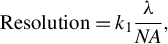 $$\begin{align}\mathrm{Resolution}={k}_1\frac{\lambda }{NA},\\[1.8pt] \nonumber \end{align}$$
where $\lambda$
is the wavelength of the exposure light source and
$\lambda$
is the wavelength of the exposure light source and ${k}_1$
is the process constant. Currently, the lithography machine with the shortest working wavelength uses 13.5 nm (2% bandwidth) extreme ultraviolet (EUV) light. Generally, there are four ways to produce 13.5 nm EUV radiation: synchrotron radiation source, discharge produced plasma (DPP), laser-assisted discharge plasma (LDP) and laser-produced plasma (LPP). Among them, the synchrotron radiation source[
Reference Zong, Hu, Wang, Wang, Zhang, Bo, Peng and Xu
3
] can produce high-power EUV radiation with no debris, but the device structure is complex and expensive; the DPP[
Reference Tomie and Micro-Nanolith
4
] and LDP[
Reference Teramoto, Santos, Mertens, Kops, Kops, van Wezyk, Yabuta, Nagano, Shirai, Ashizawa, Nakamura and Kasama
5
] methods will lead to heat load and corrosion on the electrodes, resulting in damage to the key components; relatively, the light source generated by LPP[
Reference Lin, Yang, Chen, Wei, Wang, Zhao, Peng and Leng
6
] is much more stable, and the amount of debris is less than with DPP, making it the mainstream of extreme ultraviolet lithography (EUVL) light sources.
${k}_1$
is the process constant. Currently, the lithography machine with the shortest working wavelength uses 13.5 nm (2% bandwidth) extreme ultraviolet (EUV) light. Generally, there are four ways to produce 13.5 nm EUV radiation: synchrotron radiation source, discharge produced plasma (DPP), laser-assisted discharge plasma (LDP) and laser-produced plasma (LPP). Among them, the synchrotron radiation source[
Reference Zong, Hu, Wang, Wang, Zhang, Bo, Peng and Xu
3
] can produce high-power EUV radiation with no debris, but the device structure is complex and expensive; the DPP[
Reference Tomie and Micro-Nanolith
4
] and LDP[
Reference Teramoto, Santos, Mertens, Kops, Kops, van Wezyk, Yabuta, Nagano, Shirai, Ashizawa, Nakamura and Kasama
5
] methods will lead to heat load and corrosion on the electrodes, resulting in damage to the key components; relatively, the light source generated by LPP[
Reference Lin, Yang, Chen, Wei, Wang, Zhao, Peng and Leng
6
] is much more stable, and the amount of debris is less than with DPP, making it the mainstream of extreme ultraviolet lithography (EUVL) light sources.
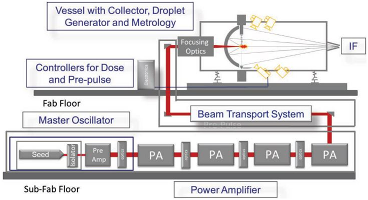
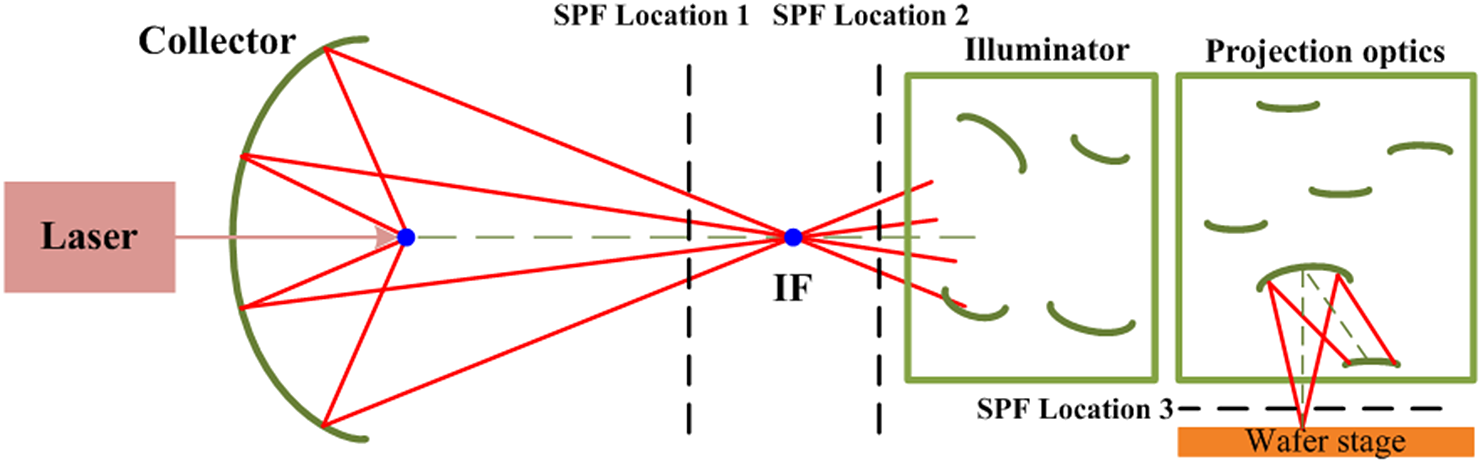
The LPP-EUVL light source system mainly consists of three parts, which are the driving laser, Sn droplet targets and the collector, as shown in Figure 1. The light source system is designed in the shape of an ellipse-of-revolution[
Reference Kriese, Platonova, Ehlersa, Jianga, Rodrigueza, Muellerb, Danielb, Khatrib, Magruderb, Granthamc, Tarrioc and Lucatortoc
8
], with one focus where Sn droplets are hit and the other far away from the collector, called the intermediate focus (IF). The pre-pulse laser (e.g., 1064 nm neodymium-doped yttrium aluminium garnet (Nd:YAG) laser) firstly gasifies and partially ionizes the droplet target, and then the main-pulse laser (e.g., 10.6 μm ${\mathrm{CO}}_2$
laser) completely ionizes the steam group to produce stronger EUV radiation[
Reference Rollinger
9
]. After that, the collector concentrates and reflects the radiations to the IF for the subsequent optical path propagation[
Reference Bakshi
10
].
${\mathrm{CO}}_2$
laser) completely ionizes the steam group to produce stronger EUV radiation[
Reference Rollinger
9
]. After that, the collector concentrates and reflects the radiations to the IF for the subsequent optical path propagation[
Reference Bakshi
10
].
Schematic of the LPP-EUVL source system. Reprinted from Ref. [Reference Fomenkov, Schafgans and Brandt7].
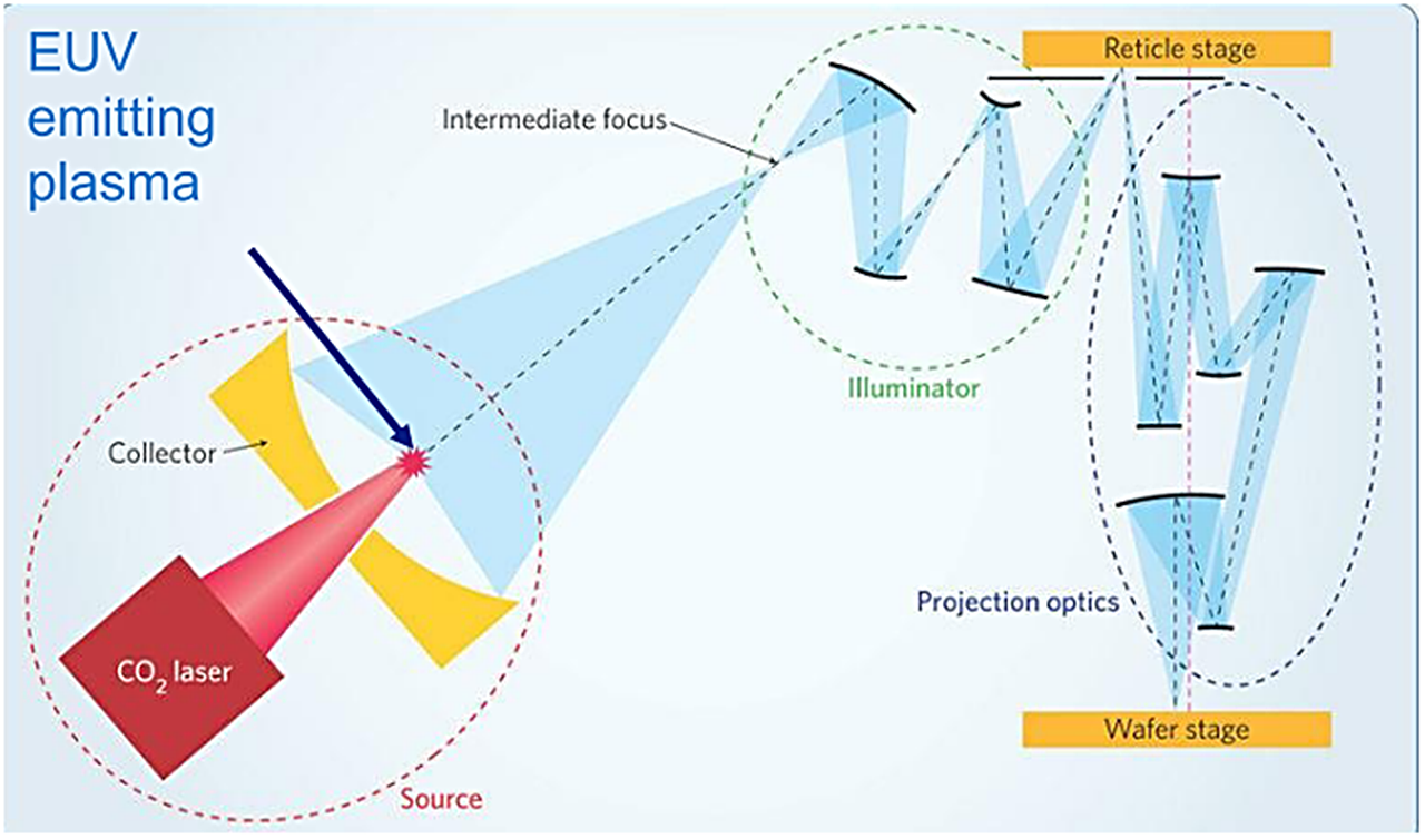
As one of the most important sub-modules, the collector is a multilayer-coated mirror that is in the shape of the graded ellipsoid with 5.5 sr[ Reference Fomenkov, Schafgans and Brandt 7 , Reference Yang, Wang, Huang, Song, Wu, Li, Wang, Tang, Xu, Liu and Gui 11 , Reference Bakshi 12 ]. With it, the EUV radiation generated can be collected and concentrated to the IF, as shown in Figure 2. In order to satisfy the actual production requirements of EUV radiation with high efficiency, high power and high purity, the collector needs to meet some design specifications[Reference Kriese, Platonova, Ehlersa, Jianga, Rodrigueza, Muellerb, Danielb, Khatrib, Magruderb, Granthamc, Tarrioc and Lucatortoc8], such as having a large enough solid collecting angle of 5.5 sr[Reference Fomenkov, Schafgans and Brandt7, Reference Yang, Wang, Huang, Song, Wu, Li, Wang, Tang, Xu, Liu and Gui11, Reference Bakshi12 ] and a highly reflective multilayer coating, as well as some specific designs to reduce the thermal load of the collector, such as a water-cooling device. However, a collector meeting the above requirements at the same time can also transmit out-of-band (OoB) radiations, that is, radiations other than 13.5 nm (2% band) EUV radiation. Once the OoB radiations are introduced or generated, the light collected and reflected by the collector will no longer be pure, which will not only influence the lithography performance, but also reduce the lifetime of the collector. Thus, it is necessary to design a spectral purity filter (SPF) in the EUVL system to filter out these OoB radiations.
Role of the collector in the light source system: the collector collects radiations and reflects them to the IF for subsequent optical path propagation. Reprinted from Ref. [Reference Wagner and Harned13].
In the past few years, different types of SPFs for EUVL have been designed and manufactured, and some have shown good performance. However, there are no comprehensive reviews or analyses of the research in this field to reflect the latest progress and the existing problems for further study. This paper reviews and discusses the technologies of filtering out OoB radiations in the LPP-EUVL system. Firstly, the influences of OoB radiations on the lithography performance are given. Then, the principles and recent progress of SPFs for EUVL are reviewed and introduced from the aspect of free-standing systems and built-in systems. Major challenges needed to be solved, including the OoB suppression, and manufacturing process as well as different metrologies, etc., are discussed. The technical routes of ASML and Gigaphoton, Inc., are specifically discussed. Finally, the future development of SPFs for EUVL is expected in the view of practical applications.
2 Out-of-band radiations of the extreme ultraviolet lithography light source
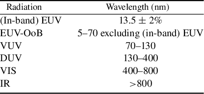
In the light source system, the driven laser hits each Sn droplet target twice to completely ionize it and generate EUV radiation. However, this process not only generates EUV radiation, but also introduces OoB radiations, which are listed in Table 1.
Radiations in the EUVL light source[ Reference Liu, van de, Bayraktar, Bijkerk, Smeets, Huang, Ni, Yakunin, Havermans, Oesterholt, Torretti, Scheers and Versolato 14 ].
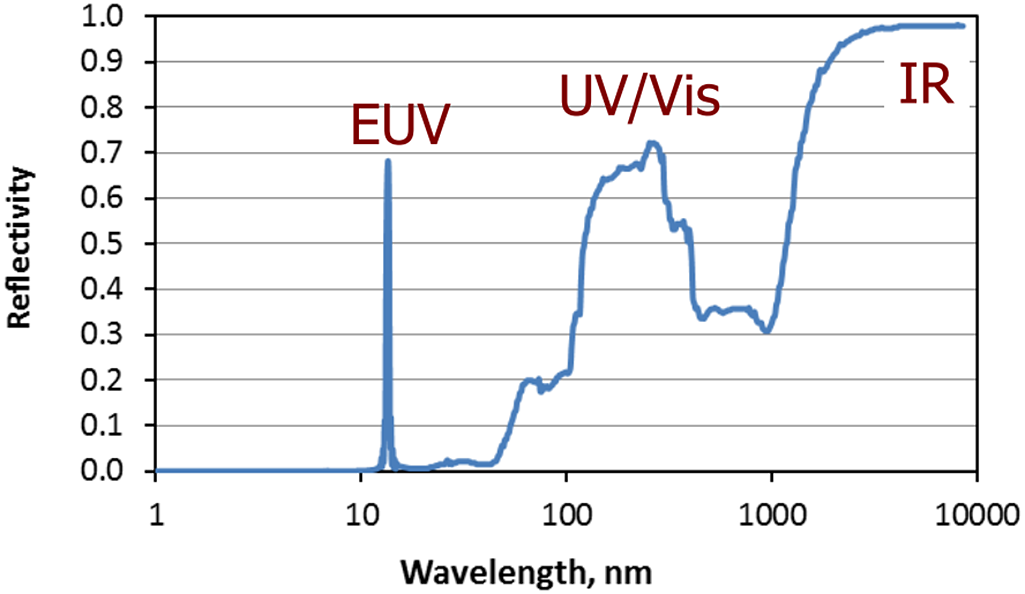
At present, the collector is generally deposited with Mo/Si multilayers to achieve high EUV reflectivity[ Reference Yang, Wang, Huang, Song, Wu, Li, Wang, Tang, Xu, Liu and Gui 11 ]. Figure 3 shows the reflectivity of Mo/Si multilayers to different radiations. It can be found that the EUV reflectivity is close to 70%, while the EUV-OoB reflectivity is so low that it can be neglected. The reflectivity of the ultraviolet (UV)/visible (VIS) spectrum is relevant to EUV radiation, and the reflectivity of infrared (IR) radiation is nearly 100%. If all of these OoB radiations are reflected by the collector and propagate to the subsequent optical path, the performance of the system will be greatly reduced.
Calculated reflectance of the 50-bilayer Mo/Si multilayer coating of 6.9 nm periodicity. Reprinted from Ref. [Reference Platonov, Kriese, Crucet, Li, Martynov, Jiang, Rodriguez, Mueller, Daniel, Khatri, Magruder, Grantham, Tarrio and Lucatorto15].
For the vacuum ultraviolet (VUV) radiations, they are effectively removed by the background hydrogen, which is originally designed for debris mitigation[ Reference van de Kerkhof, Liu, Meeuwissen, Zhang, de Kruif, Davydova, Schiffelers, Waelisch, van Setten, Varenkamp, Ricken, de Winter, McNamara, Bayraktar, Felix and Lio 16 ]. The deep ultraviolet (DUV) radiation above 300 nm (i.e., 300–400 nm) in the VIS spectrum has little impact on the lithography performance because the specifically designed photoresistor is generally insensitive to it[ Reference van de Kerkhof, Liu, Meeuwissen, Zhang, Bayraktar, de Kruif, Davydova and Micro-Nanolith 17 ]. In fact, the radiations that have a significant influence on lithography are IR and DUV radiations (130–300 nm). Therefore, most filters in the EUVL system are mainly designed for these two wavelength ranges.
2.1 Infrared radiation
IR radiation comes from the driving lasers (i.e., 10.6 μm ${\mathrm{CO}}_2$
lasers and 1064 nm Nd:YAG lasers) of the LPP-EUVL light source[
Reference Bayraktar, van Goor, Boller and Bijkerk
18
]. When generating EUV radiation, the redundant IR radiation of the lasers will also be reflected by the collector and propagated by all the following mirrors, as shown in Figure 2. In the case of the main-pulse
${\mathrm{CO}}_2$
lasers and 1064 nm Nd:YAG lasers) of the LPP-EUVL light source[
Reference Bayraktar, van Goor, Boller and Bijkerk
18
]. When generating EUV radiation, the redundant IR radiation of the lasers will also be reflected by the collector and propagated by all the following mirrors, as shown in Figure 2. In the case of the main-pulse ${\mathrm{CO}}_2$
laser with the power of approximately 20 kW, there is approximately 10% of the power (i.e.,
${\mathrm{CO}}_2$
laser with the power of approximately 20 kW, there is approximately 10% of the power (i.e., $\sim$
2 kW) that can be collected at the IF[
Reference Suzuki, Totsu, Moriyama, Esashi and Tanaka
19
]. Such high-power radiation will lead to the heating phenomenon[
Reference Bayraktar, van Goor, Boller and Bijkerk
18
,
Reference Park, Kim, Kim, Kim, Hwang, Kang, Park, Kim, Yeo and Kim
20
,
Reference Park, Kim, Kim, Kim, Hwang, Kang, Park, Kim, Yeo and Kim
21
] of optics, reticles and wafers, which may cause severe optical distortion and reduce pattern accuracy. For example, since the redundant IR radiation at the IF can be three to five times that of the EUV radiation, the overlay error may exceed eight times the specification[
Reference Soer, Jak, Yakunin, Herpen and Banine
22
]. The other problem is that the mirror heating may lead to the mutual diffusion of multilayers, photon-assisted oxidation[
Reference George, Naulleau, Rekawa, Gullikson and Kemp
23
], etc., and these will reduce the lifetime of the optics or even destroy them.
$\sim$
2 kW) that can be collected at the IF[
Reference Suzuki, Totsu, Moriyama, Esashi and Tanaka
19
]. Such high-power radiation will lead to the heating phenomenon[
Reference Bayraktar, van Goor, Boller and Bijkerk
18
,
Reference Park, Kim, Kim, Kim, Hwang, Kang, Park, Kim, Yeo and Kim
20
,
Reference Park, Kim, Kim, Kim, Hwang, Kang, Park, Kim, Yeo and Kim
21
] of optics, reticles and wafers, which may cause severe optical distortion and reduce pattern accuracy. For example, since the redundant IR radiation at the IF can be three to five times that of the EUV radiation, the overlay error may exceed eight times the specification[
Reference Soer, Jak, Yakunin, Herpen and Banine
22
]. The other problem is that the mirror heating may lead to the mutual diffusion of multilayers, photon-assisted oxidation[
Reference George, Naulleau, Rekawa, Gullikson and Kemp
23
], etc., and these will reduce the lifetime of the optics or even destroy them.
Therefore, the intensity of IR radiation is required to be less than 10% of the EUV radiation at the wafer to prevent damage, which means it needs to be 0.2% or even less of the EUV radiation at the IF[ Reference Bakshi 10 , Reference Bakshi 12 ].
2.2 Deep ultraviolet radiation
The Sn droplet target hit by the laser will ionize and produce Sn plasma. EUV radiations are generated by the ion transition of ${\mathrm{Sn}}^{7+}-\mathrm{Sn}^{10+}$
, whereas DUV radiations are mainly generated by
${\mathrm{Sn}}^{7+}-\mathrm{Sn}^{10+}$
, whereas DUV radiations are mainly generated by ${\mathrm{Sn}}^{1+}$
,
${\mathrm{Sn}}^{1+}$
, ${\mathrm{Sn}}^{2+}$
and
${\mathrm{Sn}}^{2+}$
and ${\mathrm{Sn}}^{3+}$
[
Reference van de Kerkhof, Liu, Meeuwissen, Zhang, de Kruif, Davydova, Schiffelers, Waelisch, van Setten, Varenkamp, Ricken, de Winter, McNamara, Bayraktar, Felix and Lio
16
]. The resistance is very sensitive to the DUV radiation from 150 to 300 nm[
Reference van de Kerkhof, Liu, Meeuwissen, Zhang, Bayraktar, de Kruif, Davydova and Micro-Nanolith
17
,
Reference Lorusso, Davydova, Eurlings, Kaya, Peng, Feenstra, Fedynyshyn, Natt, Huber, Zaczek, Young, Graeupner and Hendrickx
24
], which may lead to unwanted background exposure of the resistance, resulting in the loss of image contrast and critical dimension (CD) bias[
Reference van de Kerkhof, Liu, Meeuwissen, Zhang, de Kruif, Davydova, Schiffelers, Waelisch, van Setten, Varenkamp, Ricken, de Winter, McNamara, Bayraktar, Felix and Lio
16
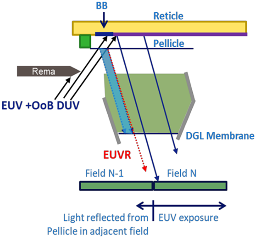
,
Reference van de Kerkhof, Liu, Meeuwissen, Zhang, Bayraktar, de Kruif, Davydova and Micro-Nanolith17]. As depicted in Figure 4, in the exposure system, the DUV reflection at the black border (BB) on a reticle will overexpose the corners and edges of the adjacent field. What is more, in order to prevent the reticle from being polluted, a pellicle is placed on the surface of it. ASML has already invented a pellicle with 90.6% EUV transmissivity[
Reference Salmaso and Maas
26
]. This kind of pellicle has a higher reflectivity of DUV radiation than the BB, so it will have a greater impact on the CD at the corners and edges[
Reference Liu, van de, Bayraktar, Bijkerk, Smeets, Huang, Ni, Yakunin, Havermans, Oesterholt, Torretti, Scheers and Versolato
14
]. However, in practice, wavelengths below 250 nm are usually suppressed due to the reflection of mirrors in the illumination and projection systems[
Reference van de Kerkhof, Liu, Meeuwissen, Zhang, de Kruif, Davydova, Schiffelers, Waelisch, van Setten, Varenkamp, Ricken, de Winter, McNamara, Bayraktar, Felix and Lio
16
], so DUV radiation plays a limited role.
${\mathrm{Sn}}^{3+}$
[
Reference van de Kerkhof, Liu, Meeuwissen, Zhang, de Kruif, Davydova, Schiffelers, Waelisch, van Setten, Varenkamp, Ricken, de Winter, McNamara, Bayraktar, Felix and Lio
16
]. The resistance is very sensitive to the DUV radiation from 150 to 300 nm[
Reference van de Kerkhof, Liu, Meeuwissen, Zhang, Bayraktar, de Kruif, Davydova and Micro-Nanolith
17
,
Reference Lorusso, Davydova, Eurlings, Kaya, Peng, Feenstra, Fedynyshyn, Natt, Huber, Zaczek, Young, Graeupner and Hendrickx
24
], which may lead to unwanted background exposure of the resistance, resulting in the loss of image contrast and critical dimension (CD) bias[
Reference van de Kerkhof, Liu, Meeuwissen, Zhang, de Kruif, Davydova, Schiffelers, Waelisch, van Setten, Varenkamp, Ricken, de Winter, McNamara, Bayraktar, Felix and Lio
16
,
Reference van de Kerkhof, Liu, Meeuwissen, Zhang, Bayraktar, de Kruif, Davydova and Micro-Nanolith17]. As depicted in Figure 4, in the exposure system, the DUV reflection at the black border (BB) on a reticle will overexpose the corners and edges of the adjacent field. What is more, in order to prevent the reticle from being polluted, a pellicle is placed on the surface of it. ASML has already invented a pellicle with 90.6% EUV transmissivity[
Reference Salmaso and Maas
26
]. This kind of pellicle has a higher reflectivity of DUV radiation than the BB, so it will have a greater impact on the CD at the corners and edges[
Reference Liu, van de, Bayraktar, Bijkerk, Smeets, Huang, Ni, Yakunin, Havermans, Oesterholt, Torretti, Scheers and Versolato
14
]. However, in practice, wavelengths below 250 nm are usually suppressed due to the reflection of mirrors in the illumination and projection systems[
Reference van de Kerkhof, Liu, Meeuwissen, Zhang, de Kruif, Davydova, Schiffelers, Waelisch, van Setten, Varenkamp, Ricken, de Winter, McNamara, Bayraktar, Felix and Lio
16
], so DUV radiation plays a limited role.
The black border’s influence on CD errors of the corners and edges of the adjacent field. Reprinted from Ref. [Reference Romanets, Ricken, Kupers, Wahlisch, Piliego, Proman, de Graaf, Behringer and Finders25].
In contrast to IR radiation, the intensity of DUV radiation is related to the characteristics of the droplet, the laser effects and even some unknown elements, such as the optical column reflectivity of DUV radiation and the DUV emission angular dependency of the plasma[ Reference van de Kerkhof, Liu, Meeuwissen, Zhang, de Kruif, Davydova, Schiffelers, Waelisch, van Setten, Varenkamp, Ricken, de Winter, McNamara, Bayraktar, Felix and Lio 16 ]. Thus, the DUV performance is generally evaluated with dose-to-clear exposure measurement at the wafer level rather than the IF point [ Reference van de Kerkhof, Liu, Meeuwissen, Zhang, de Kruif, Davydova, Schiffelers, Waelisch, van Setten, Varenkamp, Ricken, de Winter, McNamara, Bayraktar, Felix and Lio 16 , Reference Lorusso, Davydova, Eurlings, Kaya, Peng, Feenstra, Fedynyshyn, Natt, Huber, Zaczek, Young, Graeupner and Hendrickx 24 ]:
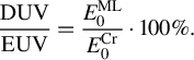 $$\begin{align}\frac{\mathrm{DUV}}{\mathrm{EUV}}=\frac{E_0^{\mathrm{ML}}}{E_0^{\mathrm{Cr}}}\cdot 100\%.\end{align}$$
The ratio of DUV and EUV radiation is determined by the dose-to-clear exposure measurement from both the multilayers and chromium of the reticle. To meet the qualification of EUVL, the value is limited to less than 1% at the wafer[ Reference Bakshi 10 , Reference Bakshi 12 ].
3 Free-standing spectral purity filters
Since IR and DUV radiations greatly degrade the performance of lithography, it is necessary to filter them out to keep high spectral purity. In the past few years, different kinds of SPFs have been designed and applied in the EUVL system. They can be generally divided into two kinds: free-standing systems and built-in systems. The former refer to filters that serve as independent devices in the source system, including the transmissive SPF and reflective SPF. The latter refer to structures that are integrated with the collector, which will be discussed in Section 4.
3.1 Transmissive SPF
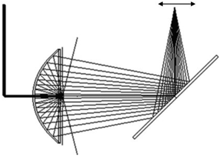
A transmissive SPF, which has the structure of periodic multilayers of high and low refractive index materials, is designed to reflect or absorb OoB radiations but transmit EUV radiations. Typical transmissive SPFs include foil filters[ Reference Bibishkin, Chkhalo, Gusev, Kluenkov, Lopatin, Luchin, Pestov, Salashchenko, Shmaenok, Tsybin and Zuev 27 ], grid filters[ Reference Suzuki, Totsu, Moriyama, Esashi and Tanaka 19 , Reference Soer, Jak, Yakunin, Herpen and Banine 22 ], etc. The transmissive SPF is usually placed before or after the IF, but in some special cases, it is placed between the projection optics and the wafer, as depicted in Figure 5. The transmissive SPF for commercial EUVL needs to meet three primary requirements, namely maintaining high transparency at 13.5 nm (Â ± 2%), effectively suppressing OoB radiation and possessing sufficient mechanical strength.
EUVL system with possible locations for the transmissive SPF.
To achieve high EUV transmissivity, a transmissive SPF needs to remain high transparency at 13.5 nm (2%) over a long working time. In contrast to monolayer films, intermetallic membranes have a better performance in IR suppression[
Reference Chkhalo, Orlikovsky, Drozdov, Kluenkov, Lopatin, Luchin, Pestov, Salashchenko, Shmaenok and Tsybin
28
], and thus multilayers composed of different high-transparency materials are studied. Andreev et al.
[
Reference Andreev, Kluenkov, Lopatin, Luchin, Prokhorov, Salashchenko, Suslov and Zuev
29
] compared the performance of filters for EUV radiation, which are constructed with Zr/Si, Nb/Si, Mo/Si or Mo/C multilayers. Bibishkin et al.
[
Reference Bibishkin, Chkhalo, Gusev, Kluenkov, Lopatin, Luchin, Pestov, Salashchenko, Shmaenok, Tsybin and Zuev
27
] fabricated a Zr/Si filter with the transparency of 76%, and achieved an EUV transmittivity of 78% and suppression ratios from 1000 (UV) to 25 (near IR). Chkhalo et al. [Reference Chkhalo, Orlikovsky, Drozdov, Kluenkov, Lopatin, Luchin, Pestov, Salashchenko, Shmaenok and Tsybin28
] later found that adding a metallic coating layer and using silicide instead of silicon can relieve the oxidation effect in multilayers. Therefore, they fabricated a $\mathrm{Zr}/{\mathrm{ZrSi}}_2$
filter coated with
$\mathrm{Zr}/{\mathrm{ZrSi}}_2$
filter coated with ${\mathrm{MoSi}}_2$
and its transparency only decreased by 4.8%, while the uncoated one decreased by about 10%. Subsequently, they substituted Zr layers with Mo layers and achieved a better performance with an in-band transparency above 70%[
Reference Chkhalo, Drozdov, Kluenkov, Lopatin, Luchin, Salashchenko, Tsybin, Sjmaenok, Banine, Yakunin and Micro-Nanolith
30
]. Notably, choosing proper materials is a trade-off among EUV transparency, OoB suppression and mechanical strength. Although some materials perform well in transparency, their mechanical strength is not ideal for high-power lasers, such as
${\mathrm{MoSi}}_2$
and its transparency only decreased by 4.8%, while the uncoated one decreased by about 10%. Subsequently, they substituted Zr layers with Mo layers and achieved a better performance with an in-band transparency above 70%[
Reference Chkhalo, Drozdov, Kluenkov, Lopatin, Luchin, Salashchenko, Tsybin, Sjmaenok, Banine, Yakunin and Micro-Nanolith
30
]. Notably, choosing proper materials is a trade-off among EUV transparency, OoB suppression and mechanical strength. Although some materials perform well in transparency, their mechanical strength is not ideal for high-power lasers, such as $\mathrm{Mo}/{\mathrm{MoSi}}_2$
multilayers[
Reference Chkhalo, Orlikovsky, Drozdov, Kluenkov, Lopatin, Luchin, Pestov, Salashchenko, Shmaenok and Tsybin
28
].
$\mathrm{Mo}/{\mathrm{MoSi}}_2$
multilayers[
Reference Chkhalo, Orlikovsky, Drozdov, Kluenkov, Lopatin, Luchin, Pestov, Salashchenko, Shmaenok and Tsybin
28
].
To withstand a long-time heat load, a filter needs to have enough mechanical strength to ensure that it will not be broken by radiations. Bibishkina et al.
[
Reference Bibishkin, Chkhalo, Gusev, Kluenkov, Lopatin, Luchin, Pestov, Salashchenko, Shmaenok, Tsybin and Zuev
27
] manufactured filters with different structures to improve the mechanical strength, such as a simple filter with a rigid framework, an improved structure with a mesh structure or a rigid mesh structure. However, these filters still cannot meet the requirements of commercial EUVL. To go further, Soer et al.
[
Reference Soer, Jak, Yakunin, Herpen and Banine
22
] developed a honeycomb grid SPF with an EUV transmittance of 72% at normal incidence, which can stand a ${\mathrm{CO}}_2$
laser power density of 100 W/cm2 for 8 hours. Suzuki et al.
[
Reference Suzuki, Totsu, Moriyama, Esashi and Tanaka
19
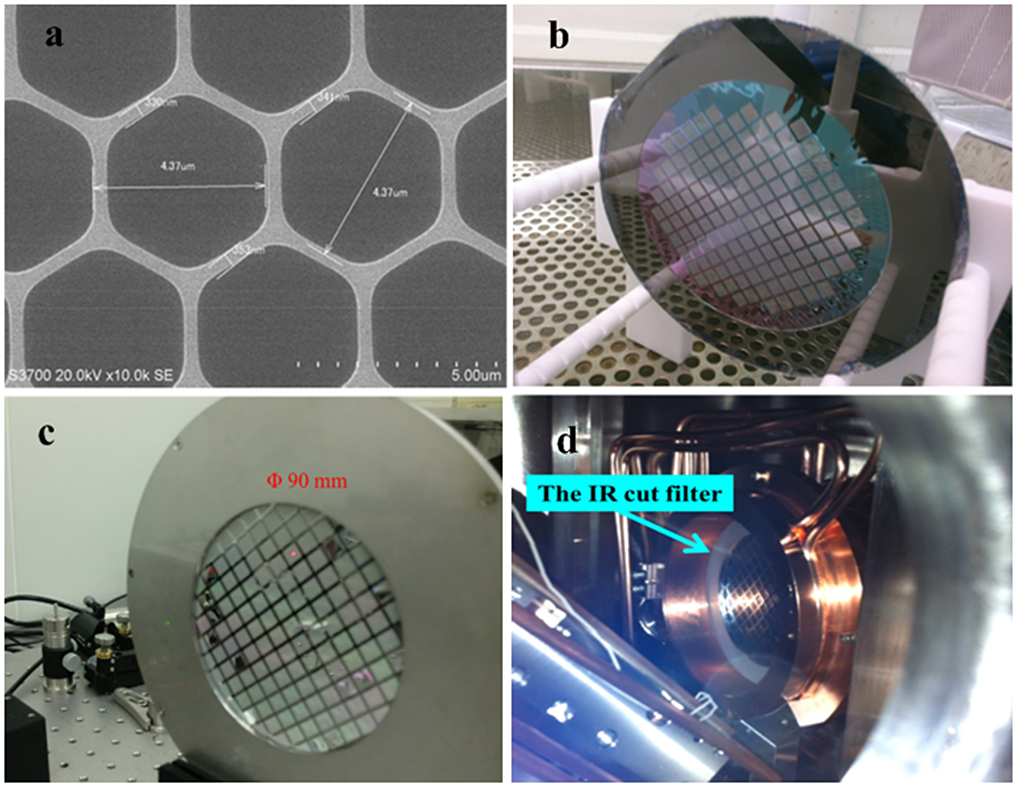
] also adopted the honeycomb grid structure to produce an IR cut-off filter with a diameter of 90 mm for an EUV light source, as shown in Figure 6, and finally achieved 99.7% suppression for 10.6 μm, but the transmittance of EUV radiation is about 78%, which still leads to considerable EUV loss.
${\mathrm{CO}}_2$
laser power density of 100 W/cm2 for 8 hours. Suzuki et al.
[
Reference Suzuki, Totsu, Moriyama, Esashi and Tanaka
19
] also adopted the honeycomb grid structure to produce an IR cut-off filter with a diameter of 90 mm for an EUV light source, as shown in Figure 6, and finally achieved 99.7% suppression for 10.6 μm, but the transmittance of EUV radiation is about 78%, which still leads to considerable EUV loss.
Grid transmissive SPF of IR suppression: (a) scanning electron microscopy image of the grid after etching, (b) grid SPF after backside wet etching, (c) grid SPF with a diameter of 90 mm installed for measurement and (d) grid SPF installed in the LPP source system. Adapted from Ref. [Reference Suzuki, Totsu, Moriyama, Esashi and Tanaka19].
3.1.1 ASML’s technical route
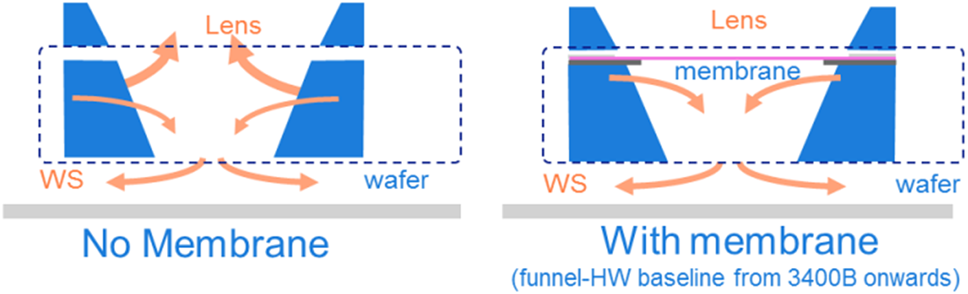
In the EUVL system of ASML, the reticle is protected from being contaminated by covering a pellicle on it that has a higher reflectivity to DUV radiation than the BB, resulting in a greater impact on CD errors. To reduce its influence, a free-standing transmissive SPF, which is called a dynamic gas lock membrane (DGLm), is adopted by ASML in NXE:3400. Figure 7 depicts the details of the DGLm. The DGLm is mainly composed of four different layers[ Reference van de Kerkhof, Jasper, Levasier, Peeters, van Es, Bosker, Zdravkov, Lenderink, Evangelista, Broman, Bilski and Last 32 ], of which DUV and IR active layers are the core of the whole membrane to filter out the OoB radiations. Different from most transmissive SPFs’ locations, the DGLm is located between the projection optics and the wafer. With this design, the DGLm acts as a physical barrier to prevent the contamination of projection optics caused by resistance outgassing[ Reference Es, van de Kerkhof, Minnaert, Fisser, Klerk, Smits, Moors, Verhoeven, Levasier, Peeters, Pieters and Meiling 33 ]. The DGLm is a free-standing device, and thus it can be replaced once damaged. What is more, as the membrane is placed further away from the IF, it is less sensitive to non-uniform transmission and particles[ Reference van de Kerkhof, Jasper, Levasier, Peeters, van Es, Bosker, Zdravkov, Lenderink, Evangelista, Broman, Bilski and Last 32 ].
DGL's location and its influence on outgassing suppression. Reprinted from Ref. [Reference Fomenkov31].
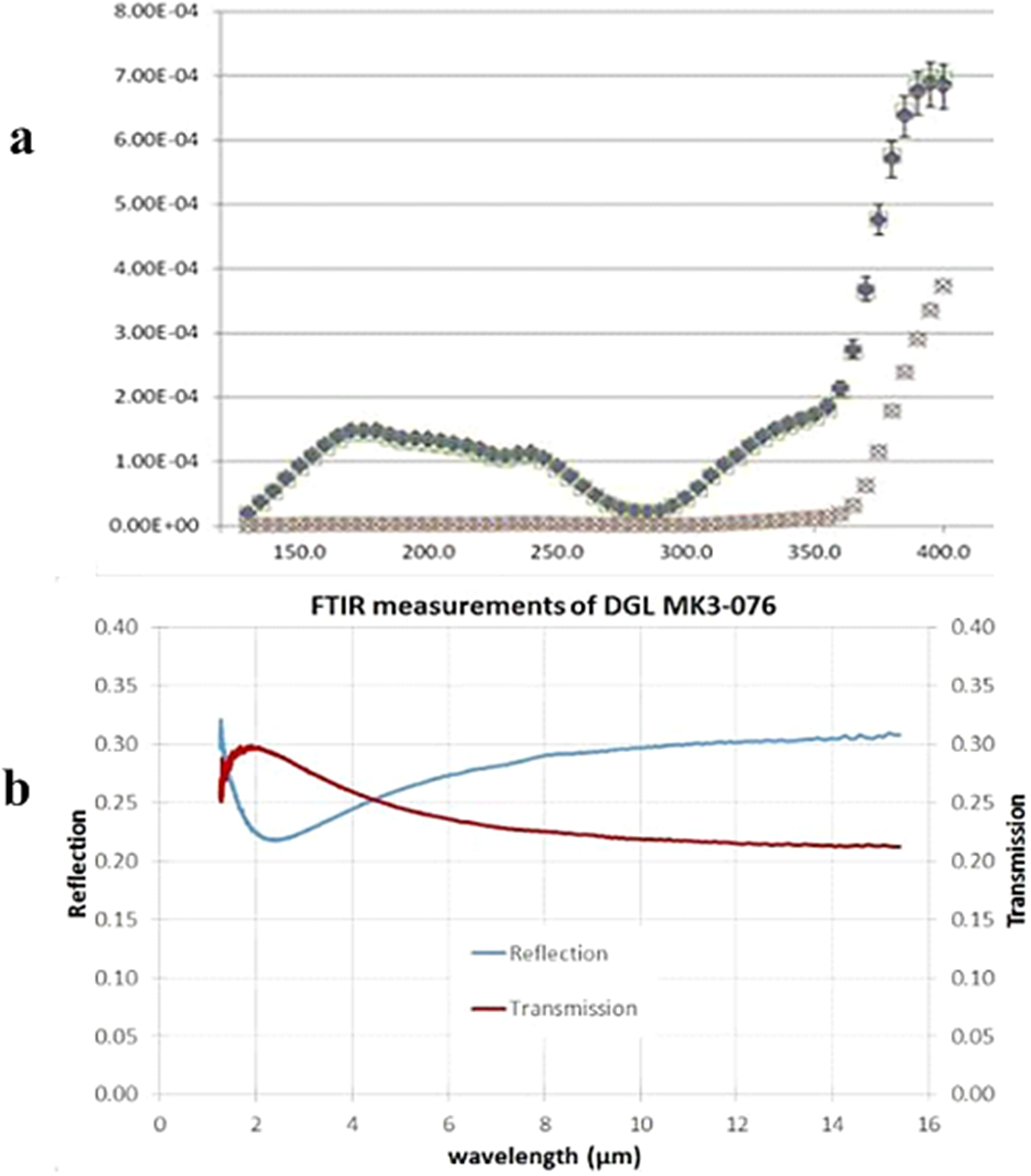
With the design of the DGLm, more than 99% DUV and nearly 80% IR radiations can be suppressed[ Reference van de Kerkhof, Jasper, Levasier, Peeters, van Es, Bosker, Zdravkov, Lenderink, Evangelista, Broman, Bilski and Last 32 ], as depicted in Figure 8. Since the total thickness of the membrane is below 50 nm and the absorption coefficient of the material is low, the EUV transmittance can reach 85%[ Reference van de Kerkhof, Jasper, Levasier, Peeters, van Es, Bosker, Zdravkov, Lenderink, Evangelista, Broman, Bilski and Last 32 ]. Without the DGLm, the CDs at the corners and edges are all less than 0.1 nm, which has already met the requirements of the N5 node, while with the DGLm, the CD reaches approximately 0.04 nm[ Reference van de Kerkhof, Liu, Meeuwissen, Zhang, de Kruif, Davydova, Schiffelers, Waelisch, van Setten, Varenkamp, Ricken, de Winter, McNamara, Bayraktar, Felix and Lio 16 ], which represents an improvement of DUV suppression. It should be noted that the excellent performance without the DGLm is based on the suitable solutions of other EUVL components, such as the specific designs of the BB and the sensitive enough resistance, but the DGLm can improve the DUV suppression under conditions that are not good enough, such as with less sensitive resistance. However, a potential problem is that the OoB light is not filtered until it enters the wafer stage; hence, the mirrors in the optical path will be damaged by the high-power radiation.
OoB suppression performance with DGLm: (a) complete suppression of DUV radiation (<0.1% transmitted) as measured by PTB; (b) 78% IR suppression as measured off-line by Fourier transform infrared spectroscopy. Adapted from Ref. [Reference Fomenkov31].
3.2 Reflective SPF
The reflective SPF is designed to reflect EUV radiation, but diffract or absorb the OoB light. It is usually a composite grating structure with multilayers deposited on the surface. A typical study by Kierey et al.
[
Reference Kierey, Heidemann, Kleemann, Winters, Singer, Melzer, Wevers and Antoni
34
] manufactured a blazed grating SPF, which is composed of grating segments with different linear densities. The blazed grating is made of NG5 black glass and coated with an Ru layer. Its blazed angle is optimized to ${1.2}^{\circ}\pm {0.2}^{\circ }$
. One of the segments was measured on BESSY II, which showed that the EUV reflectivity reached 57% at the incident angle of
${1.2}^{\circ}\pm {0.2}^{\circ }$
. One of the segments was measured on BESSY II, which showed that the EUV reflectivity reached 57% at the incident angle of ${83}^{\circ }$
. The structure of the free-standing reflective SPF allows it to be designed onto the EUV collector, so the relevant researches on it are mainly focused on the early stage, which also provided a certain theoretical basis for the collector integrated with a grating structure. They will be discussed in combination with built-in SPFs in Section 4.
${83}^{\circ }$
. The structure of the free-standing reflective SPF allows it to be designed onto the EUV collector, so the relevant researches on it are mainly focused on the early stage, which also provided a certain theoretical basis for the collector integrated with a grating structure. They will be discussed in combination with built-in SPFs in Section 4.
Comparing the above two SPFs, it can be found that the reflective SPF has better robustness and can be designed on the collector to reduce one optical element, although the EUV reflectivity may be limited to the collector efficiency (i.e., 70%). The advantage of the transmissive SPF is that it does not change the optical path of EUV radiation, so the design of the optic system has little or even no impact. Nevertheless, both two SPFs are free-standing devices that are easily broken by the OoB light, especially IR radiation. Therefore, built-in spectral purity filtering systems have been proposed and have become one of the mainstream schemes.
4 Integrated spectral purity filters on the collector
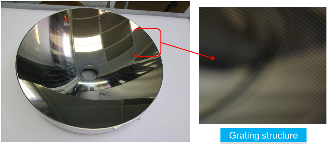
The built-in SPF system refers to a collector integrated with grating structures, as shown in Figure 9. This design not only reduces an optical element in the light source system, but also has better mechanical strength, and the water-cooled device fabricated on the collector in some designs also reduces the thermal effect. There are mainly two technical routes of fabricating gratings on collectors[ Reference Zhang 35 ]: one is to etch/deposit gratings on multilayers, which is introduced in Section 4.2, while the other is to fabricate gratings directly on the collector substrate, followed by coating, which is introduced in Section 4.3. The latter method is one of the mainstream methods, and has already been maturely applied to the EUVL light source system[ Reference Kriese, Platonova, Ehlersa, Jianga, Rodrigueza, Muellerb, Danielb, Khatrib, Magruderb, Granthamc, Tarrioc and Lucatortoc 8 , Reference Feigl, Perske, Pauer, Fiedler, Zeitner, Leitel, Eckstein, Schleicher, Schröder, Trost, Risse, Steinkopf, Scholze and Laubis 36 , Reference Nakarai, Abe, Tanaka, Watanabe, Hori, Kodama, Shiraishi, Yanagida, Soumagne, Yamada and Saitou 37 ].
Collector with a grating structure from Gigaphoton, Inc. Reprinted from Ref. [Reference Platonov, Kriese, Crucet, Li, Martynov, Jiang, Rodriguez, Mueller, Daniel, Khatri, Magruder, Grantham, Tarrio and Lucatorto15].
4.1 Principles
The principles of the collector integrated with gratings are based on the Bragg reflection by the multilayers and the diffraction due to the predetermined grating shapes[ Reference Moriya, Wakabayashi and Soumagne 38 ].
4.1.1 Bragg diffraction
The EUV collector is also known as a Bragg reflector[ Reference van den Boogaard, van Goor, Louis and Bijkerk 39 ] for the design of coating Mo/Si multilayers on the surface of the collector to maximize the EUV reflectivity. The Bragg reflector is an optical device that uses the constructive interference of reflected light at different interfaces to enhance the reflection of specific wavelengths[ Reference Kittel and McEuen 40 , Reference Haase 41 ]. According to the Bragg’s law, when the optical path difference of the reflected light at two adjacent interfaces is half a wavelength, the reflected light at the interface will incur constructive interference and get a strong reflection[ Reference Migura 42 ]. The formula formation of Bragg’s law in the case of periodic multilayers[ Reference Guen, André, Wu, Ilakovac, Delmotte, de Rossi, Bridou, Meltchakov, Giglia and Nannarone 43 , Reference Moseley 44 ] is as follows:
 $$\begin{align}2d\sin \theta = n\lambda,\\[-20pt] \nonumber\end{align}$$
where $d$
is the multilayer period,
$d$
is the multilayer period, $\theta$
is the incident angle,
$\theta$
is the incident angle, $n$
is diffraction order and
$n$
is diffraction order and $\lambda$
is the incident wavelength. The reflectivity is determined by the number of layers and the refractive index difference between materials.
$\lambda$
is the incident wavelength. The reflectivity is determined by the number of layers and the refractive index difference between materials.
4.1.2 Grating diffraction
Grating diffraction is generally based on the Fraunhofer multi-slit diffraction effect. Once the optical path difference from the two adjacent slits to the interference point is an integral multiple of the wavelength of the incident light, the two beams have the same phase and the interference will be enhanced[ Reference Kittel and McEuen 40 ]. The grating equation summarizes the phenomenon:
 $$\begin{align}p\left(\sin \delta +\sin \theta \right)= m\lambda, \end{align}$$
where $p$
is the grating period,
$p$
is the grating period, $\delta$
is the diffraction angle,
$\delta$
is the diffraction angle, $\theta$
is the incident angle,
$\theta$
is the incident angle, $m$
is the diffraction order and
$m$
is the diffraction order and $\lambda$
is the wavelength of the incident light. With proper grating designs according to the grating equation, the needed radiation can be concentrated around one specific diffraction order, and most of the OoB radiation is diffracted to other orders[
Reference Feigl, Perske, Pauer, Fiedler, Zeitner, Leitel, Eckstein, Schleicher, Schröder, Trost, Risse, Steinkopf, Scholze and Laubis
36
,
Reference Medvedev, van den Boogaard, van der Meer, Yakshin, Louis, Krivtsun and Bijkerk
45
,
Reference Miles, McCoy, McEntaffer, Eichfeld, Lavallee, Labella, Drawl, Liu, DeRoo and Steiner
46
].
$\lambda$
is the wavelength of the incident light. With proper grating designs according to the grating equation, the needed radiation can be concentrated around one specific diffraction order, and most of the OoB radiation is diffracted to other orders[
Reference Feigl, Perske, Pauer, Fiedler, Zeitner, Leitel, Eckstein, Schleicher, Schröder, Trost, Risse, Steinkopf, Scholze and Laubis
36
,
Reference Medvedev, van den Boogaard, van der Meer, Yakshin, Louis, Krivtsun and Bijkerk
45
,
Reference Miles, McCoy, McEntaffer, Eichfeld, Lavallee, Labella, Drawl, Liu, DeRoo and Steiner
46
].
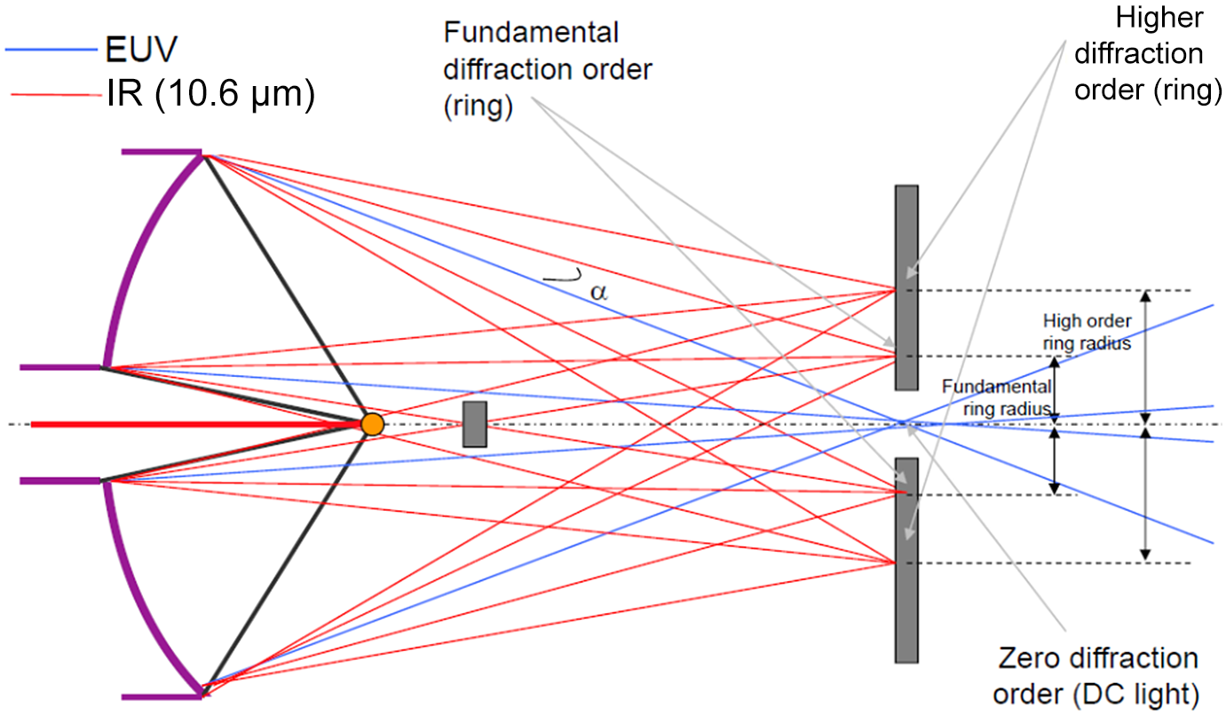
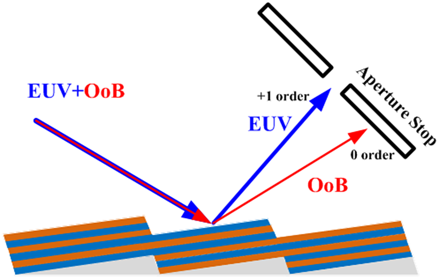
Figure 10 shows the schematic of the OoB suppression design with the built-in SPF system, in which the blue line is the beam path of EUV radiation, while the red line is OoB radiation. After the laser radiations hit the Sn droplets, the EUV radiation is generated and the OoB radiations travel to the collector firstly. With the effect of the grating coated with Mo/Si multilayers, the EUV radiation concentrated at the zero order is reflected to the IF for the subsequent propagation, while the IR radiation is diffracted to higher diffraction orders and stopped by the beam stop.
Schematic of the IR suppression design with the collector integrated with the rectangular substrate grating. Adapted from Ref. [Reference Mizoguchi, Nakarai, Abe, Nowak, Kawasuji, Tanaka, Watanabe, Hori, Kodama, Shiraishi, Yanagida, Soumagne, Yamada, Yamazaki, Okazaki and Saitou47].
4.2 Multilayer gratings
The multilayer grating refers to etching/depositing multilayers in the shape of gratings on the substrate of the collector[ Reference Huang, de Boer, Barreaux, Paardekooper, van den Boogaard, van de Kruijs, Zoethout, Louis and Bijkerk 48 , Reference Trost, Schroder, Duparre, Risse, Feigl, Zeitner and Tunnermann 49 ]. Spiller[ Reference Spiller 50 , Reference Spiller 51 ] first suggested using reflective multilayers to improve the EUV reflectivity of the grating[ Reference Naulleau, Liddle, Salmassi, Anderson and Gullikson 52 ]. Figure 11 depicts the schematic of the rectangular multilayer grating. The rectangular grating is not only easy to fabricate, but also effective to suppress the specific wavelength, and thus it is often considered as a good solution to the built-in SPF system. Van den Boogaard et al. [ Reference van den Boogaard, van Goor, Louis and Bijkerk 39 ] generated a Mo/Si rectangular multilayer grating reflector for EUVL that provided a 64% EUV reflectivity with a 30 times suppression at 280 nm. Trost et al. [ Reference Trost, Schroder, Duparre, Risse, Feigl, Zeitner and Tunnermann 49 ] designed a Mo/Si multilayer grating that generated only 0.04% IR radiation with an EUV reflectivity of 53% at zero order. Medvedev et al. [ Reference Medvedev, van den Boogaard, van der Meer, Yakshin, Louis, Krivtsun and Bijkerk 45 ] adopted the lift-off contact lithography process to fabricate the multilayer grating and achieved 61% EUV reflectivity with 70 times suppression at 10 μm. The process allowed a much shorter grating period to meet a better angular separation for EUV and OoB radiations. However, the rectangular multilayer grating can only be used to suppress a single wavelength, and is difficult to achieve high EUV diffraction efficiency (DE) while eliminating OoB radiation.
Schematic of the rectangular multilayer grating.
Compared with the rectangular grating, the blazed grating can suppress a wider range of wavebands[ Reference Huang, Medvedev, van de Kruijs, Yakshin, Louis and Bijkerk 53 ], as shown in Figure 12. Naulleau et al. [ Reference Naulleau, Sweattb and Tichenorc 54 ] analysed the main factors that affect the EUV and OoB efficiency in the EUVL light source system, and proposed a theoretical efficiency analysis of the blazed grating SPF. Van den Boogaard et al. [ Reference van den Boogaard, Louis, van Goor and Bijkerk 20 ] demonstrated theoretically that the full spectral separation can be obtained without losing EUV reflectance if the multilayer performance is not influenced by the process. Generally, the DE of the multilayer blazed grating is affected by the quality of the saw-tooth facets, smoothness of the substrate and groove density, and the former two are the main challenges. Naulleau et al. [ Reference Naulleau, Liddle, Salmassi, Anderson and Gullikson 52 , Reference Naulleau, Liddle, Anderson, Gullikson, Mirkarimi, Salmassi and Spiller 55 , Reference Naulleau, Anderson, Gullikson and Bokor 56 ] proposed a method of fabricating the blazed grating and decreased the roughness caused by the substrate by smoothing the optimized multilayers, which presented an evident smoothing effect, while it was at the cost of the profile fidelity. Naulleau et al. [ Reference Naulleau, Liddle, Anderson, Gullikson, Mirkarimi, Salmassi and Spiller 55 ] and Liddle et al. [ Reference Liddle, Salmassi, Naulleau, Gullikson and Vac 57 ] identified the conditions for topography control while fabricating the blazed grating with hydrogen silsesquioxane (HSQ), and achieved a relative EUV efficiency of 63%. Voronov et al. [ Reference Voronov, Anderson, Gullikson, Salmassi, Warwick, Yashchuk and Padmore 58 ] optimized the growth of Mo/Si multilayers by varying the sputtering gas pressure, and improved the DE from 39.6% to 44.0%. The same group[ Reference Voronov, Gullikson, Salmassi, Warwick and Padmore 59 ] then founded that the reduction of the groove density and the high-order operation can lead to higher efficiency. A 52% EUV DE was obtained at the second order with a 2525 lines/mm blazed grating. Miles et al. [ Reference Miles, McCoy, McEntaffer, Eichfeld, Lavallee, Labella, Drawl, Liu, DeRoo and Steiner 46 ] expounded the methodology of manufacturing the blazed grating and raised a way to replicate the grating, which obtained 65% DE at the first order. However, although numerous methods are raised to improve the process, it is still too difficult to meet the requirements, and thus the DE of the blazed grating is far from the theoretical limit.
Schematic of the blazed multilayer grating.
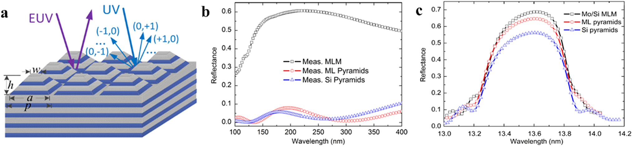
A new pyramid structure with a feasible process method, such as half-shadowing, has been proposed to suppress the full DUV band, as shown in Figure 13. Initially, a 2D pyramid structure made of Si that was deposited on Mo/Si multilayers was preferred. Huang et al. [ Reference Huang, Paardekooper, Zoethout, Medvedev, van de Kruijs, Bosgra, Louis and Bijkerk 61 ] studied the mechanism of a pyramid structure suppressing DUV radiation, and the Si pyramid showed 0.1%–10.5% DUV reflectivity, which was about 14 times suppression compared with the non-structured collector, and the EUV’s peak reflectivity reached 56.2%. To reduce the loss of EUV radiation, the Mo/Si multilayer pyramid was proposed to replace the Si pyramid and the EUV reflectivity was up to 64.7%, while the DUV response was the same as that of the Si pyramid[ Reference Huang, de Boer, Barreaux, Paardekooper, van den Boogaard, van de Kruijs, Zoethout, Louis and Bijkerk 48 , Reference Huang, de Boer, Barreaux, van der Meer, Louis and Bijkerk 60 ]. Although the multilayer pyramid grating shows good performance within DUV filtering and EUV reflectivity, this structure has not been made and tested on the EUVL collector to the authors’ knowledge, and the performance in IR filtering also has not been studied.
2D pyramid multilayer grating on the collector: (a) design of the multilayer pyramids; (b) UV-suppression performance of Si pyramids and the Mo/Si multilayer mirror in (a); (c) EUV performance comparison of Si pyramids and the Mo/Si multilayer mirror in (a). Adapted from Refs. [Reference Huang, Medvedev, van de Kruijs, Yakshin, Louis and Bijkerk53,Reference Huang, de Boer, Barreaux, van der Meer, Louis and Bijkerk60].
The multilayer grating provides a method to integrate the grating structure with the collector, and has been widely studied in recent years. The key point, as well as the difficulty, of this technology is to develop a suitable process for stacking multilayers without degrading the EUV reflectivity[ Reference Feigl, Perske, Pauer, Fiedler, Zeitner, Leitel, Eckstein, Schleicher, Schröder, Trost, Risse, Steinkopf, Laubis and Scholze 62 ]. In particular, the rectangular grating on the collector requires about 500 pairs of layers[ Reference Trost, Schroder, Duparre, Risse, Feigl, Zeitner and Tunnermann 49 , Reference Feigl, Perske, Pauer, Fiedler, Zeitner, Leitel, Eckstein, Schleicher, Schröder, Trost, Risse, Steinkopf, Laubis and Scholze 62 ] with smooth surfaces, steep edges, etc., and this largely reduces the feasibility of using multilayer gratings as the SPF.
4.3 Substrate gratings
The substrate grating refers to the case in which the surface of the collector substrate is firstly fabricated in the shape of the grating, and then the multilayers are deposited[ Reference Zhang 35 , Reference Feigl, Perske, Pauer, Fiedler, Zeitner, Leitel, Eckstein, Schleicher, Schröder, Trost, Risse, Steinkopf, Laubis and Scholze 62 ]. The method has advantages. It reduces an optical element in the light source system, has a good mechanical strength and avoids the process difficulty of stacking hundreds of layers. This scheme has already been applied to the collector by Gigaphoton, Inc.[ Reference Nakarai, Abe, Tanaka, Watanabe, Hori, Kodama, Shiraishi, Yanagida, Soumagne, Yamada and Saitou 37 , Reference Mizoguchi 63 – Reference Mizoguchi, Nakarai, Abe, Tanak, Watanabe, Hori, Shiraishi, Yanagida, Sumangne, Yamada, Saitou, Felix and Lio 65 ]. They adopted the rectangular grating as the substrate grating to filter out the IR radiation of 10.6 μm and 1064 nm, and achieved only 0.37% IR reflectivity[ Reference Mizoguchi, Nakarai, Abe, Nowak, Kawasuji, Tanaka, Watanabe, Hori, Kodama, Shiraishi, Yanagida, Soumagne, Yamada, Yamazaki, Okazaki and Saitou 47 , Reference Nakarai, Abe, Nowak, Kawasuji, Tanaka, Watanabe, Hori, Kodama, Shiraishi, Yanagida, Soumagne, Yamada, Yamazaki and Saitou 66 ], while the EUV reflectivity only reduced by approximately 4% compared with the mirror without a grating structure[ Reference Nakarai, Abe, Tanaka, Watanabe, Hori, Kodama, Shiraishi, Yanagida, Soumagne, Yamada and Saitou 37 ].
This section will mainly discuss the rectangular substrate grating, including the design principles, fabrication process and the metrology. Gratings of other shapes will also be introduced briefly as a supplement in Section 4.3.4.
4.3.1 Design principles
Assume that the OoB radiation that needs to be suppressed is 10.6 μm and the grating is in the shape of a 1D rectangle. As Figure 14 shows, the grating is characterized by the period $p$
, width
$p$
, width $d$
and depth
$d$
and depth $h$
of the grooves. When the 13.5 nm EUV radiation combined with the 10.6 μm is incident onto the grating, if the diffraction order
$h$
of the grooves. When the 13.5 nm EUV radiation combined with the 10.6 μm is incident onto the grating, if the diffraction order $m=0$
, both radiations’ reflection angles are the same, while with higher diffraction orders, the characteristic values of the diffraction angles differ by about three orders of magnitude[
Reference Medvedev, van den Boogaard, van der Meer, Yakshin, Louis, Krivtsun and Bijkerk
45
]. Therefore, the 10.6 μm radiation at m = 0 is what we need to suppress. Assuming that the grating is illuminated by the normal-incidence plane wave, the following equation shows the mth-order DE of the 1D rectangular phase grating:
$m=0$
, both radiations’ reflection angles are the same, while with higher diffraction orders, the characteristic values of the diffraction angles differ by about three orders of magnitude[
Reference Medvedev, van den Boogaard, van der Meer, Yakshin, Louis, Krivtsun and Bijkerk
45
]. Therefore, the 10.6 μm radiation at m = 0 is what we need to suppress. Assuming that the grating is illuminated by the normal-incidence plane wave, the following equation shows the mth-order DE of the 1D rectangular phase grating:
 $$\begin{align}{R}_n={R}_{\mathrm{tot}}{\left|\sin \mathrm{c}\left( m\pi \right)+A\Gamma \sin \mathrm{c}\left( m\pi \right)\right|}^2, \\[-24pt] \nonumber\end{align}$$
where ${R}_{\mathrm{tot}}$
is the total reflected intensity,
${R}_{\mathrm{tot}}$
is the total reflected intensity, $\Gamma =\frac{d}{p}$
and
$\Gamma =\frac{d}{p}$
and $A=\exp \left(\frac{i\cdot 4\pi h}{\lambda}\right)-1$
, and
$A=\exp \left(\frac{i\cdot 4\pi h}{\lambda}\right)-1$
, and
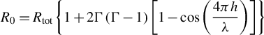 $$\begin{align}{R}_0={R}_{\mathrm{tot}}\left\{1+2\Gamma \left(\Gamma -1\right)\left[1-\cos \left(\frac{4\pi h}{\lambda}\right)\right]\right\}\end{align}$$
is the particular case of zero diffraction order, which both can be derived from Equation (2)
[
Reference Medvedev, van den Boogaard, van der Meer, Yakshin, Louis, Krivtsun and Bijkerk
45
]. To suppress the 10.6 μm IR radiation at zero order, Equation (5) should be equal to zero. It can be calculated that the fill factor $\Gamma =0.5$
and the minimum depth of the grooves is
$\Gamma =0.5$
and the minimum depth of the grooves is $h=\frac{\lambda }{4}=\sim 2.65$
μm. The period
$h=\frac{\lambda }{4}=\sim 2.65$
μm. The period $p$
is more difficult to determine because it is a trade-off between IR reflectivity at the zero order (
$p$
is more difficult to determine because it is a trade-off between IR reflectivity at the zero order ( $\sim p/\lambda$
) and the angular separation of diffraction (
$\sim p/\lambda$
) and the angular separation of diffraction ( $\sim \arcsin \left(\lambda /p\right)$
)[
Reference Medvedev, van den Boogaard, van der Meer, Yakshin, Louis, Krivtsun and Bijkerk
45
,
Reference Johnson
67
]. What is more, the limited spatial and temporal coherence of the radiation should also be considered[
Reference Medvedev, van den Boogaard, van der Meer, Yakshin, Louis, Krivtsun and Bijkerk
45
,
Reference Huang, de Boer, Barreaux, van der Meer, Louis and Bijkerk
60
].
$\sim \arcsin \left(\lambda /p\right)$
)[
Reference Medvedev, van den Boogaard, van der Meer, Yakshin, Louis, Krivtsun and Bijkerk
45
,
Reference Johnson
67
]. What is more, the limited spatial and temporal coherence of the radiation should also be considered[
Reference Medvedev, van den Boogaard, van der Meer, Yakshin, Louis, Krivtsun and Bijkerk
45
,
Reference Huang, de Boer, Barreaux, van der Meer, Louis and Bijkerk
60
].
Design of the rectangular substrate grating: (a) schematic of 1D rectangular substrate grating; (b) schematic of 2D rectangular substrate grating by IOF. Adapted from Refs. [Reference Huang, Medvedev, van de Kruijs, Yakshin, Louis and Bijkerk53,Reference Feigl, Perske, Pauer, Fiedler, Zeitner, Leitel, Eckstein, Schleicher, Schröder, Trost, Risse, Steinkopf, Laubis and Scholze62].
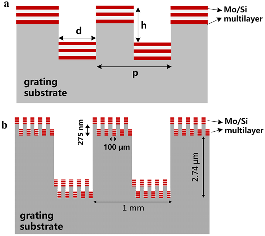
To suppress radiations of two wavelengths, in particular 10.6 μm and 1064 nm, this method can be used to determine the dual-layer grating. Since the difference between the two wavelengths is 10 times, the parameters of the grating are also 10 times different. The Fraunhofer Institute for Applied Optics and Precision Engineering (IOF)[ Reference Feigl, Perske, Pauer, Fiedler, Zeitner, Leitel, Eckstein, Schleicher, Schröder, Trost, Risse, Steinkopf, Scholze and Laubis 36 , Reference Feigl, Perske, Pauer, Fiedler, Zeitner, Leitel, Eckstein, Schleicher, Schröder, Trost, Risse, Steinkopf, Laubis and Scholze 62 ] designed and fabricated a dual-wavelength rectangular grating with optimized geometric parameters, as shown in Figure 14. At the IF, the measured reflectivity of 10.6 μm is 0.32%, the reflectivity of 1064 nm is only 0.08% and the average reflectivity of the EUV radiation at 13.5 nm is 64% which represents only 4.5% loss compared to the unstructured multilayers.
4.3.2 Fabrication process
At present, there are two main processes to fabricate the substrate gratings deposited with multilayers. The main difference between them is the preparation of the substrate grating, which involves the diamond turning process and ion beam etching.
The process of manufacturing the substrate grating used by Rigaku is the diamond turning[ Reference Platonov, Kriese, Crucet, Li, Martynov, Jiang, Rodriguez, Mueller, Daniel, Khatri, Magruder, Grantham, Tarrio and Lucatorto 15 ]. Firstly, Ni is injected into the substrate made of Al alloy and the surface of it is polished. Then the grating grooves are made on the Ni surface by diamond turning, which will result in turning patterns, as shown in Figure 15(a), and high spatial frequency roughness (HSFR) on the cut surface. Therefore, a glass smoothing layer is then needed to smooth the substrate grating. The other method, the ion beam etching process, is used by IOF[ Reference Feigl, Perske, Pauer, Fiedler, Zeitner, Leitel, Eckstein, Schleicher, Schröder, Trost, Risse, Steinkopf, Scholze and Laubis 36 , Reference Feigl, Perske, Pauer, Fiedler, Zeitner, Leitel, Eckstein, Schleicher, Schröder, Trost, Risse, Steinkopf, Laubis and Scholze 62 ] to prepare a dual-layer rectangular grating on the collector’s substrate, which is made of AlSi alloy. With the method, the substrate is firstly diamond turned and polished to reduce the HSFR to less than 0.2 nm rms, and then, the dual-layer grating is directly constructed into the NiP layer of the AlSi substrate by ion beam etching.
(a) AFM image of diamond-turned patterns and (b) the mechanical polished surface of (a). Reprinted from Ref. [Reference Trost, Schroder, Duparre, Risse, Feigl, Zeitner and Tunnermann49].
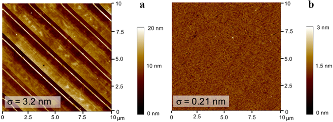
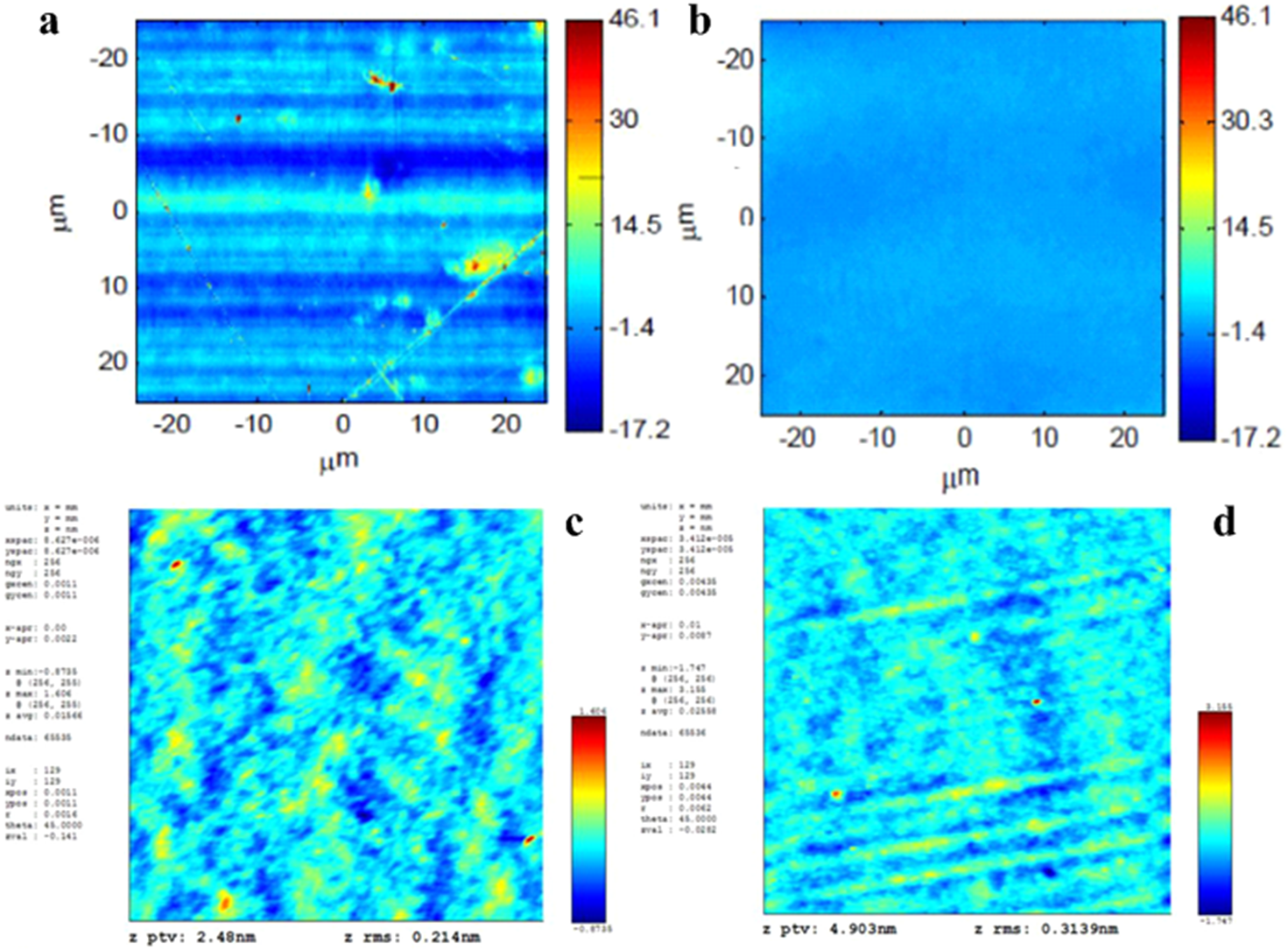
When manufacturing the substrate grating, the HSFR is a critical factor to achieve a smooth enough surface. To reduce the HSFR, some methods are proposed. Mechanical polishing[ Reference Trost, Schroder, Duparre, Risse, Feigl, Zeitner and Tunnermann 49 ] is the simplest smoothing method, which is mainly used to remove typical diamond turning structures. As shown in the Figure 15, it reduced the HSFR by more than 10 times. Ion beam polishing technology[ Reference Soer, Gawlitza, van Herpen, Jak, Braun, Muys and Banine 68 , Reference Spiller, Baker, Mirkarimi, Sperry, Gullikson and Stearns 69 ], which is commonly used on collectors without gratings, uses the neutral ion beam to bombard the workpiece, removing atoms or molecules in a certain area of the surface, and achieves ultra-smooth polishing. The method of adding a smoothing layer[ Reference Zhang 70 ] refers to manufacturing a film on the substrate with a smaller HSFR to smooth the roughness, and the performance can be seen in Figures 16(a) and 16(b). Stock et al. [ Reference Stock, Hamelmann, Kleineberg, Menke, Schmiedeskamp, Osterried, Heidemann and Heinzmann 71 ] used the electron beam evaporation method to deposit a single layer of carbon on the substrate of BK7 and Zerodur to smooth the roughness. Salmassi et al. [ Reference Salmassi, Naulleau and Gullikson 72 , Reference Salmassi, Anderson, Gullikson and Naulleau 73 ] proposed a spin-on-glass resistance process based on HSQ to smooth a substrate with diamond-turned structures and presented a roughness reduction from 3.7 nm to 0.39 nm rms on the Al substrate. Rigaku[ Reference Kriese, Platonova, Ehlersa, Jianga, Rodrigueza, Muellerb, Danielb, Khatrib, Magruderb, Granthamc, Tarrioc and Lucatortoc 8 ] used a glassy smoothing layer on the substrate grating to reduce the HSFR of the surface, achieving the results presented in Figures 16(c) and 16(d), which is sufficient for high performance. Ulmer et al. [ Reference Ulmer, Dugard, Quispe, Buchholz, Stagon, Chung, Cao, Kritikos, Guerra, Stahl, Shiri, Vaidyanathan, den Herder, Nakazawa and Nikzad 74 ] designed a mirror with a diameter of 1 m and smoothed the NiP substrate by covering the CN x layer.
HSFR results (AFM) of adding a smoothing layer by Rigaku: (a) diamond-turned surface sample; (b) smoothed diamond-turned surface sample; (c) 0.14–0.29 nm rms over 2.2 μm scans; (d) 0.29–0.39 nm rms over 8.7 μm scans of the grating surface. Adapted from Refs. [Reference Kriese, Platonova, Ehlersa, Jianga, Rodrigueza, Muellerb, Danielb, Khatrib, Magruderb, Granthamc, Tarrioc and Lucatortoc8,Reference Platonov, Kriese, Crucet, Li, Martynov, Jiang, Rodriguez, Mueller, Daniel, Khatri, Magruder, Grantham, Tarrio and Lucatorto15].
4.3.3 Metrology
During the preparation of the substrate grating, some measurements are needed to measure the machining accuracy and the overall device performance. The three main aspects to be measured are the roughness, reflectivity for different wavelengths and uniformity of reflectivity.
Roughness. The thickness of the multilayers deposited on the substrate grating is at the level of nanometres, and thus the morphology and roughness of the substrate will be translated to the top layers[ Reference Naulleau, Liddle, Anderson, Gullikson, Mirkarimi, Salmassi and Spiller 55 , Reference Zhang 70 , Reference Louis, Yakshin, Tsarfati and Bijkerk 75 ]. It is clear that the prerequisite for reducing the roughness of the multilayers is to reduce the roughness of the substrate grating. The evaluation indicators for roughness include the average roughness, root mean square (RMS) roughness, peak-to-valley (PV) value, power spectral density (PSD), etc. The first three are simple statistical parameters and only the vertical component of surface roughness is calculated[ Reference Zhang 70 ]. The PSD measures the roughness from the perspective of Fourier spectra, thereby obtaining the spatial frequency distribution of the surface error, which means it also contains the transverse and longitudinal information of the surface[ Reference Chen 76 , Reference Li 77 ].
Roughness in different spatial frequency ranges should be measured by different methods, as shown in Figure 17. According to the scattering theory, the scattering caused by roughness in different spatial frequencies can be generally divided into the following three types[Reference Louis, Yakshin, Tsarfati and Bijkerk75, Reference Yang, Zheng and Chen78–Reference Schuster, Merkel, Metalidis and Kierey80]:
-
(1) minimum angle scattering caused by low spatial frequency roughness (LSFR), which introduces basic aberration into the system, will blur the image and reduce the resolution of the optical system;
-
(2) small-angle scattering caused by medium spatial frequency roughness (MSFR), also known as stray light, will reduce the contrast of spatial imaging;
-
(3) large-angle scattering caused by HSFR will reduce the light flux reaching the image plane, thus reducing the energy transmission efficiency of the optical system.
Different measurements for roughness at different spatial frequencies. Adapted from Ref. [Reference Zhang70].
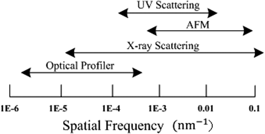
Taking Rigaku’s work as a reference[ Reference Kriese, Platonova, Ehlersa, Jianga, Rodrigueza, Muellerb, Danielb, Khatrib, Magruderb, Granthamc, Tarrioc and Lucatortoc 8 ], the different spatial frequencies of roughness, corresponding to the above influences, are defined as follows: LSFR, more than or equal to 1 mm; MSFR, 1 mm–10 μm; HSFR, less than or equal to 10 μm.
The HSFR is a critical indicator to be measured because among the roughness in all frequency bands, the roughness with the spatial wavelength equivalent to the incident light wavelength has the strongest scattering ability[
Reference Zhang
70
]. The HSFR of the grating surface used for the collector needs to be less than 0.3 nm rms[
Reference Trost, Schroder, Duparre, Risse, Feigl, Zeitner and Tunnermann
49
,
Reference Feigl, Perske, Pauer, Fiedler, Zeitner, Leitel, Eckstein, Schleicher, Schröder, Trost, Risse, Steinkopf, Laubis and Scholze
62
], which is also the main challenge of the fabrication. At present, the main and most direct method used in HSFR for measuring surfaces with less than or equal to 0.1 nm rms is atomic force microscope (AFM) measurement, which determines the distance between the probe and the detection surface by the contact force. Its detection area is usually less than tens of micrometres, the longitudinal resolution is approximately 0.01 nm[
Reference Li
77
] and the transverse resolution can generally be up to 0.1 nm[
Reference Zhang
70
,
Reference Chen
76
], which depends on the radius of curvature of the probe and the depth from the top of the probe to the detection surface[
Reference Zhang
70
,
Reference Eastman and Bausmeister
81
]. In the IOF’s experiments on the dual-layer rectangular grating[
Reference Feigl, Perske, Pauer, Fiedler, Zeitner, Leitel, Eckstein, Schleicher, Schröder, Trost, Risse, Steinkopf, Scholze and Laubis
36
,
Reference Feigl, Perske, Pauer and Fiedler
82
], with a scanning range of 10 μm $\times$
10 μm, the roughnesses of the four facets of the grating were all below 0.25 nm rms. It should be noted that if PSD is used for characterization, it is necessary to measure the same surface at different locations and meet the sampling theorem.
$\times$
10 μm, the roughnesses of the four facets of the grating were all below 0.25 nm rms. It should be noted that if PSD is used for characterization, it is necessary to measure the same surface at different locations and meet the sampling theorem.
The LSFR is primarily measured by optical profilometry, including white light interferometry (WLI), double-beam interferometry, etc., among which WLI is the main method currently used. WLI is a non-contact metrology, and has the advantages of a large measuring range, high vertical accuracy and fast measuring speed. Based on the principle of optical interference, WLI can analyse the relative height variation of the sample surface according to the contrast and position of the light interference fringe, thus generating a 3D image and obtaining the 3D morphology and surface roughness of the measured sample. However, due to the influence of dispersion, its lateral accuracy can only reach the scale of hundreds of nanometres[ Reference Chen 76 , Reference Li 77 ]. The IOF[ Reference Feigl, Perske, Pauer, Fiedler, Zeitner, Leitel, Eckstein, Schleicher, Schröder, Trost, Risse, Steinkopf, Scholze and Laubis 36 ] used the WLI to characterize the profile of its dual-layer substrate grating, as Figure 18 shows, and controlled the maximum error of the grating period, fill factor and groove depth within less than 1%. Rigaku[ Reference Kriese, Platonova, Ehlersa, Jianga, Rodrigueza, Muellerb, Danielb, Khatrib, Magruderb, Granthamc, Tarrioc and Lucatortoc 8 ] also used an interference microscope to measure the roughness of the substrate grating, and achieved an LSFR of 0.577 μm rms.
WLI analysis of a dual-layer rectangular substrate grating structure by the IOF. Reprinted from Ref. [Reference Feigl, Perske, Pauer, Fiedler, Zeitner, Leitel, Eckstein, Schleicher, Schröder, Trost, Risse, Steinkopf, Laubis and Scholze62].
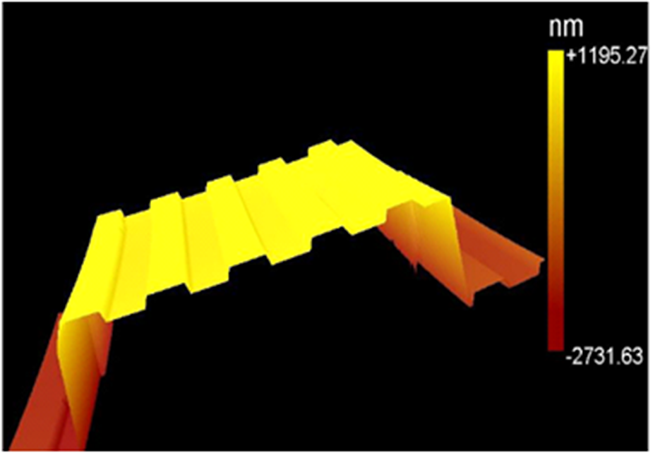
The MSFR can be measured by laser speckle interferometry and light scattering measurement, both of which are indirect measurement. The former is primarily used in the detection range where the roughness is greater than the illumination wavelength[ Reference Zhang 70 ], and has the advantages of simple operation and a large measurement range. The brightness, shape and contrast of the speckles generated by the coherent wave can effectively reflect the distribution of surface roughness. Light scattering measurement mainly includes the angle resolved scattering (ARS) measurement and total integrated scattering (TIS) measurement[ Reference Mazule, Liukaityte, Eckardt, Melninkaitis, Balachninaite and Sirutkaitis 83 ]. ARS determines the roughness according to the distribution of the scattered light intensity in the plane[ Reference Böhm, Jech and Vellekoop 84 ], while TIS determines the roughness according to the ratio of the light intensity in the hemisphere to the light intensity reflected on the surface of the sample[ Reference Wei 85 ]. Compared with TIS, ARS is more complex and expensive, but it can correctly measure the spatial distribution of scattered light and obtain more roughness information[ Reference Mazule, Liukaityte, Eckardt, Melninkaitis, Balachninaite and Sirutkaitis 83 ]. Trost et al. [ Reference Trost, Schroder, Duparre, Risse, Feigl, Zeitner and Tunnermann 49 ] used ALBATROSS (Figure 19), developed by the IOF, to measure the roughness of the multilayer grating. Hilpert et al. [ Reference Hilpert, Hartung, von Lukowicz, Herffurth and Heidler 86 ] measured the roughness of the reflector in the spaceborne optical system by ARS and obtained a roughness value of 0.1 nm rms. Herrero et al. [ Reference Herrero, Mentzel, Soltwisch, Jaroslawzew, Laubis and Scholze 87 ] of Physikalisch-Technische Bundesanstalt (PTB) exposed a new tool (EUV-ARS) based on the grazing incidence small-angle X-ray scattering instrument (Figure 20), which allows one to study the structural surface by analysing the scattered light and fluorescence signals, and to achieve the roughness measurement at the nanoscale.
ARS instrument ALBATROSS for scattering measurements in the UV-VIS-IR range. Components include laser sources (1), mechanical chopper for lock-in amplification (2), attenuation filters (3), beam preparation optics (4), polarizer (5), sample (6) and detector (7). Adapted from Ref. [Reference Feigl, Perske, Pauer, Fiedler, Zeitner, Leitel, Eckstein, Schleicher, Schröder, Trost, Risse, Steinkopf, Laubis and Scholze62].
EUV-ARS for the characterization of nanometre structures exposed by PTB. Reprinted from Ref. [Reference Herrero, Mentzel, Soltwisch, Jaroslawzew, Laubis and Scholze87].
OoB suppression and EUV reflectivity. The collector integrated with rectangular gratings is designed to suppress 10.6 μm and 1064 nm IR radiation without reducing EUV radiation, so it is necessary to detect the intensity of EUV and IR radiations at the focal plane. Compared with the collector without the grating structure, the intensity of IR radiation at the IF generally needs to be suppressed by more than 99%[ Reference Bakshi 12 ], while the minimum loss of EUV radiation achieved nowadays is approximately 4.81%[ Reference Sun, Jin, Yu, Guo, Yao, Deng and Li 88 ].
For the EUV detection, the equipment used includes the EUV reflectometry at BESSY II developed by PTB in Germany[ Reference Scholze, Laubis, Dersch, Pomplun, Burgerc and Schmidt 89 – Reference Laubis, Barboutis, Buchholz, Fischer, Haase, Knorr, Mentzel, Puls, Schönstedt, Sintschuk, Soltwisch, Stadelhoff and Scholze 92 ] (Figure 21), the EUV reflectometry by the National Institute of Standards and Technology (NIST) in the USA[ Reference Grantham, Tarrio, Lucatorto, Kriese, Platonov, Rodriguez and Jiang 93 ] and the system MERLIN of the IOF[ Reference Schröder, Herffurth, Trost and Duparré 94 ].
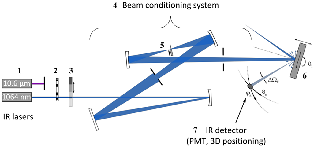
Mechanics of the EUV reflectometer by PTB. Reprinted from Ref. [Reference Scholze, Laubis, Dersch, Pomplun, Burgerc and Schmidt89].
For the detection of IR suppression, ALBATROSS[ Reference Schröder, Herffurth, Blaschke and Duparré 95 ] can also be used. In fact, ALBATROSS is a device that can measure the reflected light, transmitted light and scattered light distribution with a high dynamic range, high sensitivity and low noise. What is more, the measurement device can also be custom-built for the actual measuring needs, as shown in Figure 22. The laser firstly passes through the beam expander, chopper, etc., and is then reflected by the virtual light source sphere before being incident on the full-size collector. After being deflected by a folded plane mirror, it is focused on the HgCdTe detector for the measurement[ Reference Kriese, Platonova, Ehlersa, Jianga, Rodrigueza, Muellerb, Danielb, Khatrib, Magruderb, Granthamc, Tarrioc and Lucatortoc 8 ].
Schematic of the IR suppression test stand. Reprinted from Ref. [Reference Kriese, Platonova, Ehlersa, Jianga, Rodrigueza, Muellerb, Danielb, Khatrib, Magruderb, Granthamc, Tarrioc and Lucatortoc8].
Reflectivity uniformity. The final step in the preparation of the substrate grating is to deposit Mo/Si multilayers, which aims to improve the EUV reflection performance, so measuring the EUV reflectivity uniformity is very important. The EUV reflectometry mentioned above is used to symmetrically select multiple positions on the collector’s surface along the x- and y-axes and measure their reflectivity for comparison. The IOF[ Reference Feigl, Perske, Pauer, Fiedler, Zeitner, Leitel, Eckstein, Schleicher, Schröder, Trost, Risse, Steinkopf, Scholze and Laubis 36 ] used the system of PTB to compare the average EUV reflectivity of the collector integrated with the dual-layer grating, and the change of EUV reflectivity is approximately 0.5%. Rigaku[ Reference Kriese, Platonova, Ehlersa, Jianga, Rodrigueza, Muellerb, Danielb, Khatrib, Magruderb, Granthamc, Tarrioc and Lucatortoc 8 ] used the same system as the IOF to measure the peak EUV reflectivity of the collector surface, and showed a variation of less than 0.0025 nm at the opposite positions, referring to 0.02% PV variation.
4.3.4 Gratings with other shapes
According to the existing technical schemes, the collector substrate of the rectangular grating structure cannot effectively filter the DUV radiation, so it is proposed to use a blazed grating to replace the rectangular grating since the structure was theoretically demonstrated to be effective at filtering out full-OoB radiations by van den Boogaard et al. [ Reference van den Boogaard, Louis, van Goor and Bijkerk 20 ] when studying the multilayer grating.
Johnson[ Reference Johnson 67 , Reference Johnson and Vac 96 ] designed a collector integrated with the blazed grating structure that aims to divert the EUV radiation into the IF rather than diffracting IR radiation out of the IF, as shown in Figure 23(a), and two fabrication methods are given, which are the conformal-multilayer grating and patterned-multilayer grating. What is more, a power recycling component was designed surrounding the IF aperture to retroreflect IR radiation for a higher source conversion efficiency (CE). Following that, Hassanein et al. [ Reference Hassanein, Sizyuk, Sizyuk and Johnson 97 ] continued the design of the blazed grating and furthered the idea of power recycling, which showed a potential 60% gain of EUV-CE with the preliminary plasma simulation, as shown in Figure 23(b). However, these relevant researches based on the substrate blazed grating are mainly theoretical analyses, and no experiments have been carried out to establish the feasibility of this scheme.
(a) Schematic of the collector integrated with the blazed substrate grating and (b) schematic of the collector with power recycling mirrors. Reprinted from Refs. [Reference Johnson and Vac96,Reference Hassanein, Sizyuk, Sizyuk and Johnson97].
Theoretically, the blazed grating can indeed suppress the radiation of the IR and UV bands, but the problem lies in the limitations of the manufacturing process. For example, it is difficult to control the blazed angle of the multilayers within ${3}^{\circ }$
[
Reference Zhang
35
]. Therefore, its actual effect is far from reaching the theoretical effect, so it is still at the theoretical stage.
${3}^{\circ }$
[
Reference Zhang
35
]. Therefore, its actual effect is far from reaching the theoretical effect, so it is still at the theoretical stage.
5 Conclusions and expectations
As the most precise manufacturing process in the world today, lithography technology imposes very high requirements for the purity of its high-power EUV light source. For the LPP-EUVL system, the OoB radiation with the greatest impact is IR radiation (i.e., 1064 nm and 10.6 μm) and DUV radiation, the former of which causes the thermal effect and reduces the pattern accuracy, while the latter leads to CD errors. Therefore, the intensity of IR radiation needs to be less than 10% and that of DUV radiation needs to be only 1% of that of EUV radiation at the wafer to avoid potential damage, while the intensity of EUV radiation must be as high as possible.
Taking the above conditions as the basic indicators for evaluating the SPF for EUVL, it can be found that traditional free-standing SPFs can barely satisfy the suppression requirements of IR and DUV radiations, and also lead to an EUV loss of approximately 30%[ Reference Sun, Jin, Yu, Guo, Yao, Deng and Li 88 ]. However, some new free-standing filters have been proposed in recent years and have shown a good performance, such as the DGLm by ASML, which suppressed 99% of DUV radiation and 80% of IR radiation, while the EUV transmittance reached 85%. Although it may have problems of non-ideal mechanical strength and an extra optical element, it still shows potential as an SPF for EUVL, especially for the suppression of DUV radiation, as it produces less thermal damage to the optical elements, compared to IR radiation.
The scheme of taking the micro-structures, integrated onto the collector, as the SPF for an EUVL light source also seems to be feasible and effective, especially the substrate grating structure, which avoids the process difficulty of stacking thousands of layers. According to the achievements of current researches, Gigaphoton, Inc., has already obtained an IR suppression of 0.37% at the IF, while the reduction of EUV reflectivity with an unpolarized incident laser is only around 4% compared with the non-structured collector, which represents a better performance than free-standing SPFs. Besides that, this scheme allows a superior mechanical strength, and some designs can be applied onto the collector to relieve the thermal effect, such as a water-cooled device.
The existing designs of the collector integrated with the substrate grating still need to be optimized. For the rectangular grating, which has been studied maturely, it only suppresses finite and specific wavelengths, and there is no research showing its suppression capacity in the DUV band so far. Therefore, how to suppress IR radiation at the same time as DUV radiation is a problem that remains. There are probably three ways to go. One is to adopt the scheme of integrating the collector with the blazed substrate grating. This method raises difficulties of stacking lots of layers, which has been the challenge for years and, also, manufacturing the periodic blazed grating on such a large collector is not easy. The second is to further develop the membrane that is manageable to suppress all OoB radiations, just like DGLm, but this faces the problem of being broken easily by the thermal effect from the ${\mathrm{CO}}_2$
laser and will increase the cost of maintenance. The third is to combine the other two schemes, which means integrating the collector with rectangular gratings, while using a transmissive SPF membrane. A similar method has been explored by Suzuki et al.
[
Reference Suzuki, Totsu, Moriyama, Esashi and Tanaka
19
], but they use two free-standing SPFs (one for IR radiation and one for DUV radiation), which obviously represents less mechanical strength than the collector. Thus, there is still room for the improvement of the spectral purity of the EUV light source.
${\mathrm{CO}}_2$
laser and will increase the cost of maintenance. The third is to combine the other two schemes, which means integrating the collector with rectangular gratings, while using a transmissive SPF membrane. A similar method has been explored by Suzuki et al.
[
Reference Suzuki, Totsu, Moriyama, Esashi and Tanaka
19
], but they use two free-standing SPFs (one for IR radiation and one for DUV radiation), which obviously represents less mechanical strength than the collector. Thus, there is still room for the improvement of the spectral purity of the EUV light source.
Besides the designs of SPFs for the EUVL light source, the metrology also needs to be improved. With the development of the semi-industry, metrologies that can deal with the smaller and more complex nano-structures are needed. There is no doubt that the scattering metrology plays an important role in this field. To achieve a higher sensitivity, grazing incidence small-angle X-ray scattering is often used, but it has the problem of large footprints of the beam, which needs to be resolved in a more general solution. Using a larger incident wavelength as the source, which allows a larger incident angle, may relieve this problem without reducing the sensitivity. Herreroa et al.’s work[ Reference Herrero, Mentzel, Soltwisch, Jaroslawzew, Laubis and Scholze 87 ] gives some suggestions in this aspect. Another problem that limits the performance of the measuring is the speed of the measurement; in particular, when measuring the surface roughness, the ARS needs a lot of time to detect the scattering distribution in the hemisphere space, which can be relieved by the improvement of the scattering model to some extent, such as the regional scattering model by Wang et al. [ Reference Wang, Wei, Tian, Liu and Zhu 98 ]. Efforts shall be made on the design of the measuring devices as well as the metrologies in order to meet the requirements of measuring nano-structures.
This paper reviews the development of the SPFs for EUVL, and investigates the key technologies of filtering out OoB radiations for EUVL. The main challenges and developing trends are also discussed in view of the practical applications for further improvement. It can be seen that the design and manufacture of SPFs for EUVL is not a single task; rather, it requires a coordinated advancement in design methods, process manufacturing and metrologies.
Acknowledgement
This work was supported by the Science and Technology Commission of Shanghai Municipality (No. 22DZ1100300).


 Open access