

Introduction
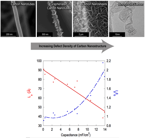
Nanostructured carbon materials have been widely studied for applications in electrochemical energy storage, including activated carbon,[Reference Frackowiak and Béguin1–Reference Gamby, Taberna, Simon, Fauvarque and Chesneau3] carbon nanotubes (CNTs),[Reference Futaba, Hata, Yamada, Hiraoka, Hayamizu, Kakudate, Tanaike, Hatori, Yumura and Iijima4–Reference Frackowiak, Metenier, Bertagna and Beguin7] and graphene.[Reference Stoller, Park, Zhu, An and Ruoff8–Reference Liu, Yu, Neff, Zhamu and Jang11] Applications of such devices include hybrid structures in automotive energy storage,[Reference Kuperman and Aharon12] flexible electronics,[Reference He, Chen, Li, Zhang, Fu, Zhao and Xie13–Reference Miller, Outlaw and Holloway15] and neural stimulation electrodes.[Reference Cogan16] In order to optimize the performance of such devices, a clear understanding of the relationship between the physical properties of nanostructured carbon materials and electrochemical capacitance is required. As a nondestructive process, determination of nanocrystalline domain size using the Raman I D/I G ratio,[Reference Tuinstra and Koenig17–Reference Dresselhaus, Jorio, Hofmann, Dresselhaus and Saito20] referred to interchangeably as graphitic cluster size or in-plane correlation length,[Reference Ferrari and Robertson21] provides a facile and inexpensive method to engineer carbon nanostructures for energy storage applications. In this study, we present a relationship between this nanocrystalline domain size and the specific capacitance of various carbon nanostructures grown by plasma-enhanced chemical vapor deposition (PECVD) and measured by Raman spectroscopy. Previous works[Reference Kim, Lim, Kwon, Hong, Qiao, Rhee, Yoon and Mochida22–Reference Ambrosi, Poh, Wang, Sofer and Pumera26] have suggested a relationship between graphitic edge planes and specific capacitance for graphite, glassy carbon, highly ordered pyrolytic graphite, carbon nanofibers, multi-walled carbon nanotubes, and doped graphene. This work is believed to be the first to quantify the relationship between structural defects, largely contributed by few-layered graphene (FLG) edge planes, and the specific capacitance in terms of nanocrystalline domain size for graphene–CNT hybrid materials. It is also believed to be the first study of its kind across materials that span such a large range of domain sizes.
Materials and methods
The details of the PECVD growth system are described elsewhere,[Reference Cui, Zhou and Stoner27] as is the deposition process for growth of the graphenated carbon nanotubes (g-CNTs) used in this study.[Reference Parker, Raut, Brown, Stoner and Glass28] In brief, nanostructures were grown in a 915 MHz microwave PECVD reactor using 50 Å Fe catalyst deposited on silicon. Prior to deposition, the substrates were heated to the desired deposition temperature in 100 sccm NH3, followed by striking and stabilizing the plasma at 21 Torr and 2.15 kW magnetron input power. The substrates were pretreated for several minutes in the ammonia plasma to dewet the Fe catalyst film to form nanoparticles. The gas flow was subsequently changed to 150 sccm CH4 and 50 sccm NH3 for the desired deposition time. The graphene and CNT formed simultaneously during the growth process. Possible mechanisms for this formation have been discussed elsewhere.[Reference Parker, Raut, Brown, Stoner and Glass28, Reference Ubnoske, Raut, Brown, Parker, Stoner and Glass29] In contrast to the high-temperature conditions of g-CNT growth, which results in a high foliate density but poor nanotube alignment, vertically aligned graphenated carbon nanotubes (VA g-CNTs) were achieved by reducing deposition temperature to 900 °C and extending deposition time to 30 min. Hierarchical structures of few-layered graphene and carbon nanotubes were created by further extending the deposition time, hereafter referred to as carbon nanosheets on carbon nanotubes or CNS-on-CNTs.
Raman spectroscopy was carried out using a Horiba Jobin Yvon LabRam ARAMIS spectrometer operating with a 633 nm HeNe laser. The D and G Raman modes were deconvolved as Lorentzian peaks and the D′ was modeled as a Gaussian peak, as suggested by Ferrari and Robertson[Reference Ferrari and Robertson21] and Mennella et al.[Reference Mennella, Monaco, Colangeli and Bussoletti30] The ratio of the D and G band intensities were calculated from the intensities of the isolated peaks. The Raman spectra of the nanostructured materials and deconvolution of the peaks are shown in Fig. 1. Scanning electron micrographs of the various nanostructures examined in this study are shown in Fig. 2. Carbon nanostructures were imaged with a FEI XL30 SEM-FEG scanning electron microscope.
Raman spectra and Lorentzian deconvolution of the first-order Raman-active modes in various carbon nanostructures grown by MPECVD. The peaks shown are the D, G, and D′ in order of increasing wavenumber.

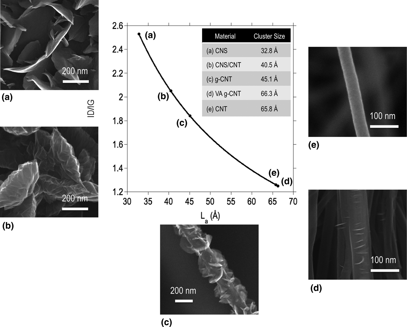
Nanocrystalline domain size in carbon nanostructures with varying degrees of disorder and graphene edge density. SEMs from (a)–(e) are CNSs, CNS-on-CNTs (plan view, underlying CNT forest not pictured), g-CNTs, VA g-CNTs, and CNTs, and the inset table lists the calculated nanocrystalline domain size for each material.
The electrochemical cell and sample preparation have been described in detail elsewhere.[Reference Raut, Parker and Glass31] A three-terminal cell (K0235 by Princeton Applied Research) was used with the nanostructure under study as the working electrode, a Pt mesh as the counter-electrode, and an Ag wire in 1 M tetrabutylammonium and 0.01 M AgNO3 in acetonitrile as the reference electrode. The electrolyte used was 1 M LiClO4 in acetonitrile. To perform electrochemical measurements, the nanostructured electrode was mounted on a piece of sheet metal using copper tape, and electrical contact was made by painting conductive silver epoxy on the nanostructure side. The nominal active area of the electrode was 1.43 cm2, defined by a PTFE gasket.
Results and discussion
Relationship between nanocrystalline domain size and nanostructure for high edge density carbon nanostructures
The classical relationship between the I D/I G ratio and nanocrystalline domain size was developed by Tuinstra and Koenig[Reference Tuinstra and Koenig17] as L a = C(I D/I G)−1, where L a is the in-plane correlation length and C = 44 Å for an excitation wavelength of λ L = 514.5 nm. Matthews et al.[Reference Matthews, Pimenta, Dresselhaus, Dresselhaus and Endo32] appended this expression to include the wavelength dependence of the constant term, where C(λ) = −126 Å + 0.033λ L for visible wavelengths. Using this expression, the nanocrystalline domain size of each material was calculated (Fig. 2). A clear correlation is observed between the nanostructure observed in the SEM and the nanocrystalline domain size as estimated from the Raman spectra. The CNS nanostructure in Fig. 2(a) contains the highest density and the thinnest nanosheets of all the samples studied, indicating that the crystalline domain size is expected to be the smallest. TEM reported elsewhere[Reference Ubnoske, Raut, Brown, Parker, Stoner and Glass29] has shown that such structures terminate in few-layered graphene, down to two or three layers. The CNS structure in Fig. 2(b) forms at the top of a CNT forest and the thickness of the nanosheets increases dramatically, while the density decreases from the samples in Fig. 2(a), indicating a larger spacing between the edges. As one observes the nanostructure evolution from Figs. 2(c) to 2(e) a decreasing density of graphene edges is observed on the g-CNT sidewalls until no foliates remain and the nanostructure is a standard vertically aligned CNT morphology. Samples shown in Figs. 2(d) and 2(e) are interesting in that both the SEM and the Raman-derived crystalline domain sizes show very minor differences. It is intriguing that the nanocrystalline domain sizes are so similar for these samples, which could imply that FLG may nucleate at the sites of previously existing defects in support of the proposed nucleation and growth model for graphene foliates.[Reference Ubnoske, Raut, Brown, Parker, Stoner and Glass29, Reference Zeng, Lei, Wang, Liang, Wang, Yao and Zhang33]
Interpretation of the nanocrystalline domain size calculation
The data in Fig. 2 and the discussion above illustrate that the observed edge density follows trends in the Raman-derived crystalline domain size. Although the Tuinstra and Koenig expression originally attempted to link the D peak intensity to phonon confinement, it has been discovered more recently that double resonance is the activation mechanism.[Reference Thomsen and Reich34] Therefore, one may consider L a as an average interdefect spacing with the expectation that a larger defect density gives rise to a higher D peak intensity, and thus a smaller L a.[Reference Ferrari35] Comparing this Raman expression with crystallite size estimates by x-ray diffraction, the larger crystallites are given less weight in this case and the above expression underestimates L a due to the dominant effect of small crystallites.[Reference Cuesta, Dhamelincourt, Laureyns, Martinez-Alonso and Tascon36–Reference Nakamizo, Kammereck and Walker38] Bearing in mind the limitations of the above formulation of crystalline domain size, the trends detailed in this letter are nevertheless tooted in the existence and spatial frequency of defects in the materials. Thus, L a can be equally referred to as the mean spacing between defects, including the edge defects that are prominent in the materials of the current study.
Relationship between nanocrystalline domain size and specific capacitance
Data from a previously reported design of experiments (DOE) study of MPECVD growth[Reference Ubnoske, Raut, Brown, Parker, Stoner and Glass29] was used to compare the I D/I G ratio and specific capacitance of a variety of carbon nanostructures from CNTs to highly defective amorphous carbon (a-C), thus extending the range of nanostructured carbons beyond those depicted in Fig. 2. Briefly, the DOE process employed statistical methods to populate the process space of growth in the PECVD reactor, analyzing catalyst thickness, pretreatment time, process gas ratio, deposition temperature, and deposition time as factors and presence of CNTs, presence of CNSs, CNT diameter, I D/I G ratio, and capacitance as responses.
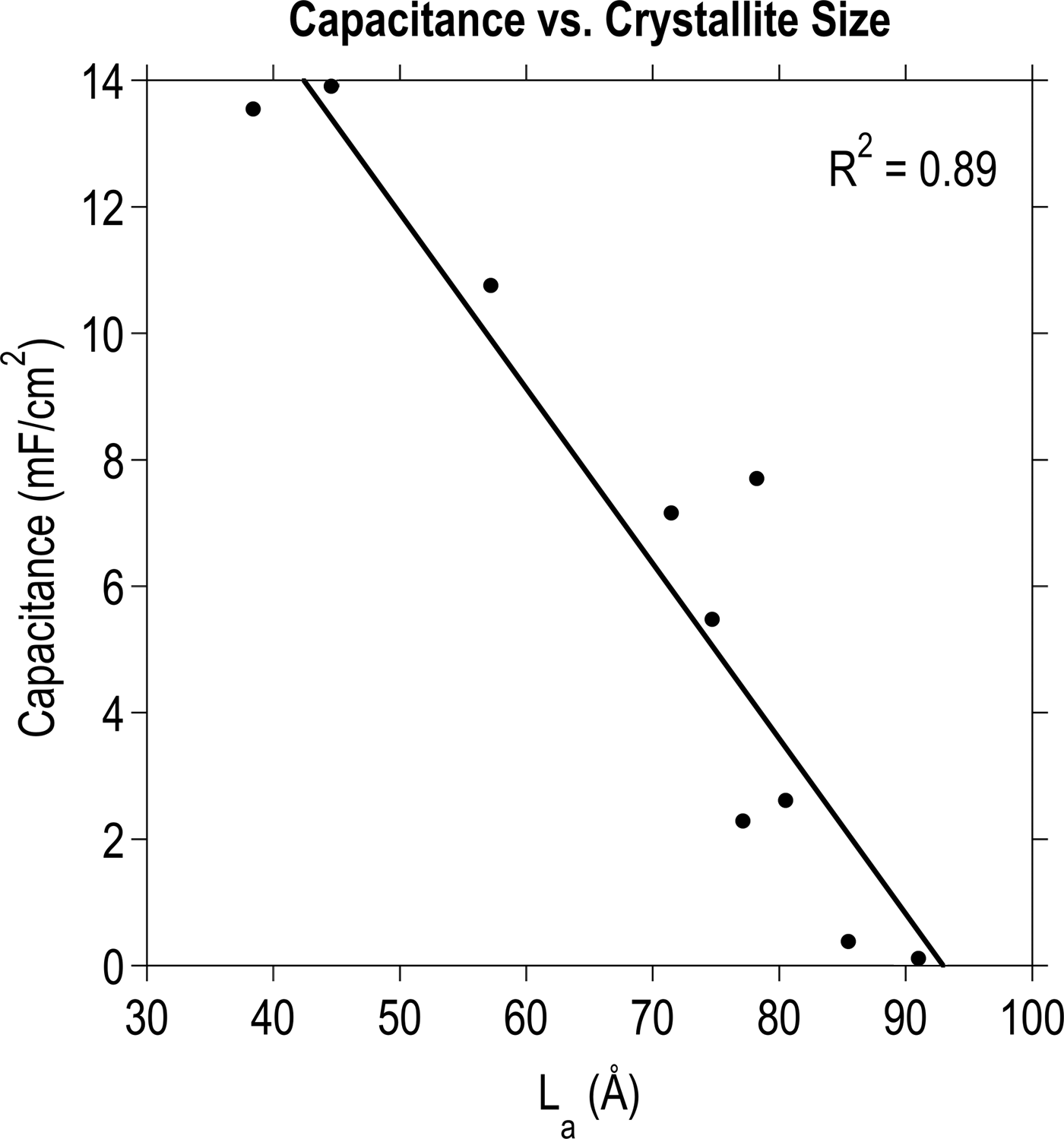
A monotonically increasing trend was discovered between I D/I G and capacitance, which prompted a comparison with L a. As can be seen in Fig. 3, a linear relationship exists between capacitance as a function of nominal surface area and the nanocrystalline domain size calculated from the Raman data. Fig. 4 illustrates this trend in the form of cyclic voltammetry (CV) curves for three representative films: CNTs, g-CNTs, and a-C. This result is in agreement with reports of Rice and McCreery[Reference Rice and McCreery23] and others[Reference Miller, Outlaw and Holloway15, Reference Rice, Pontikos and McCreery24, Reference Randin and Yeager39, Reference McCreery40] who determined that the specific capacitance of the basal plane was much lower than edge planes in graphitic materials. More recently, it was experimentally demonstrated that the edge of a single graphene sheet possesses a specific capacitance four orders of magnitude higher than the basal plane, a faster electron transfer rate, and stronger electrocatalytic activity.[Reference Yuan, Zhou, Li, Li, Peng, Zhang, Liu, Dai and Shi41] The trend is also consistent with previously reported electrochemical impedance spectroscopy data[Reference Parker, Raut, Brown, Stoner and Glass28] of g-CNTs, showing an increase of 5.4× for mass-normalized capacitance of g-CNTs compared with CNTs at 1 Hz, and faster charge transfer kinetics in g-CNTs compared with CNTs.[Reference Henry, Raut, Ubnoske, Parker and Glass42]
The relationship between nanocrystalline domain size and specific capacitance. A linear fit converges with an R 2 value of 0.89 for various carbon thin films deposited according to the DOE procedure.[Reference Ubnoske, Raut, Brown, Parker, Stoner and Glass29]
CV curves (100 mV/s) of structures from the plot in Fig. 3. SEM micrographs are representative images of the nanostructures grown for the capacitance data set, including CNTs, g-CNTs, and a-C.
By roughly estimating and comparing the surface area of CNTs and CNSs, it is possible to eliminate the possibility that the trend in Fig. 3 arises primarily due to differences in the surface area. CNSs grown by PECVD can be modeled as semi-circular two-dimensional objects with a radius of ~700 nm and inter-sheet spacing of ~500 nm based on SEM images. For a substrate of 1 cm2 nominal area, this corresponds to a surface area on the order of 10−4 m2. Similarly for CNTs on a 1 cm2 substrate, assuming a CNT diameter of ~50 nm, height ~10 μm, and density 1.5 × 10¹⁰ CNTs/cm2,[Reference Raut, Parker and Glass31] the surface area is on the order of 10−2 m2. Thus, CNTs have approximately two orders of magnitude higher surface area compared with CNSs under these experimental conditions. Since CNSs possess a smaller L a and higher specific capacitance than CNTs, it can therefore be concluded that defect density, which influences electronic structure and adsorption, more strongly corresponds to electrochemical capacitance than surface area for these materials.
The density of states (DOS) of pristine graphene, which is 0 at the Fermi level, has been shown to increase with an increase of edge plane defects.[Reference Peres, Ling and Shan-Wen43–Reference Jiang, Sumpter and Dai45] Furthermore, a high DOS was reported at graphene zig-zag edges.[Reference Jiang, Sumpter and Dai45] Interestingly, double-layered graphene is nearly 1.6 times more reactive than single-layer graphene according to calculations performed by Sharma et al.[Reference Sharma, Baik, Perera and Strano46] As the primary class of defects in the hybrid materials presented here is edge plane defects emerging from FLG foliates, an increase in local charge density at these edge plane sites may be primarily responsible for the improvement in double-layer capacitance and charge transfer kinetics. Figure 5 illustrates local differences in charge density for two simplified representative structures: a graphene flake with a pentagon defect and a small foliate covalently bonded to a CNT. Molecular orbitals and charge densities were calculated using the extended Hückel method, and energy was minimized using the MM2 interatomic potential. The edge plane sites display significantly higher charge density compared with the basal planes, in agreement with the literature.
Representation of the molecular orbitals and associated charge densities in a small graphene sheet (left) and a CNT with a graphene foliate (right) calculated using the extended Hückel method. Blue regions are more negatively charged, and red represents positively charged areas. Charge density and associated DOS are higher near the graphene edge planes relative to the basal plane, consistent with the experimental observations.
Conclusions
Carbon nanomaterials with varying defect density were grown via MPECVD and their Raman spectra were analyzed. The I D/I G ratio was used to calculate the mean nanocrystalline domain size, which may also be interpreted as the mean distance between defects or in-plane correlation length,[Reference Ferrari and Robertson21] including the “foliates” of FLG grown directly on substrates or simultaneously with CNTs. A linear trend emerged between the measured specific capacitance and L a, yielding a novel perspective for engineering carbon nanomaterials for energy storage applications.
Acknowledgments
We acknowledge Professor Tom O'Haver at the University of Maryland at College Park for development of the Matlab peak fitting script used in this study, and the Shared Materials Instrumentation Facility staff at Duke University for access to the Raman spectrometer and scanning electron microscope. This work was partially supported by grants ECCS–1344745 and DMR–1106173 from the National Science Foundation and 1R21NS070033-01A1 from the National Institutes of Health.


 Open access