


I. INTRODUCTION
The low-frequency (LF) noise at the output of a detector may contribute to increasing system instability, becoming a source of error, for example in the operation of radiometers. Particularly, to establish appropriate switching frequencies in switched radiometer systems, it is especially relevant to know the knee frequency of devices [Reference Mennella, Bersanelli, Butler, Maino, Mandolesi and Morgante1]. The presence of a switching frequency in these systems transforms the noise analysis into a cyclostationary problem. Moreover, the system's knee frequency may vary depending on the operation mode of the devices. Rigorous mathematical treatment of several types of deterministic and random signals flowing through a nonlinearity is a classic topic [Reference Middleton2], which should be reconsidered as simulation tools evolve and the requirements of systems become stricter. On the other hand, in general, apart from phase noise (PHN) in oscillators, simulation tool studies have paid limited attention to LF noise. Therefore, it is considered of great interest to have an accurate characterization of devices’ LF noise together with reliable simulation tools for predicting its conversion to the system output, depending on the device operation regimes.
The relevance of the device operation regime is shown in [Reference Graffeuil, Liman, Muraro and Llopis3], which provides empirical evidence of the shot noise deviation with respect to the conventional model in a large-signal pumped Schottky diode, proposing an alternative model based, not on the mean current of the device, but on the small-signal resistance, supported by a classic reference [Reference Dragone4] and in agreement with the distinction between shot noise with constant and with time-varying rate presented in [Reference Demir5]. In [Reference Conte, Bertazzi, Guerrieri, Bonani and Ghione6], the simulation of cyclostationary noise is treated from a physically-based point of view. In [Reference Pascual, Aja, De La Fuente, Pomposo and Artal7], the use of time-domain and transient-envelope tools is proposed for the simulation of switching radiometer systems handling noisy broadband signals. Nevertheless, the frequency domain is usually preferred for noise simulation in presence of multiple frequencies, being particularly suitable for cyclostationary noise [Reference Ngoya8]. In [Reference Ngoya8], a global modeling of cyclostationary noise simulation is proposed, including both conventional approaches (noise Modulated first, then Filtered – MF – or noise Filtered first, then Modulated – FM – as termed in [Reference Conte, Bertazzi, Guerrieri, Bonani and Ghione6]) as particular cases. The Volterra series formalism has been successfully proved as a tool to analyze the response of nonlinear systems, particularly those with memory, such as diode-based detectors, to harmonic and Gaussian (noisy) inputs [Reference Bedrosian and Rice9, Reference Gomes, Testera, Carvalho, Fernández-Barciela and Remley10]. In this work, dc current dependence of shot noise and flicker noise is revised, and a further step is proposed, from the single-device noise model to the detector noise performance under different operation regimes. The capability and limitations of harmonic balance (HB) based on commercial simulation tools to cope with these simulations is analyzed.
Three different scenarios for the characterization of diodes, alone or in detectors, are considered:
– Characterization of a single diode, to obtain the basic 1/f noise coefficients, depending only on dc bias point.
– Characterization of a microwave detector built with the same type of diode plus radio frequency (RF) input matching, dc return, and lowpass resistance capacitance (RC) output filtering. The detector is usually conceived to avoid requiring dc bias, although a bias network was added to allow dc bias and/or the measurement of rectified current through the diode due to RF and modulation pumping.
The operation regime of the detector depends on both the input and the bias conditions. Three possible inputs can be considered: a room temperature matched 50 Ω load without applied RF signal, a continuous wave (CW) RF signal or an RF amplitude modulated (AM) signal can also be applied. A dc bias can be applied or not to the diode in each of the previous cases. RF noise conversion to LF noise at the output will also be discussed.
– Characterization of a differential setup formed by two detectors. The goal of this setup is to try to cancel noise at the output coming from the RF pumping signal. In this case no external bias was applied to the detectors and the main emphasis was put on the shot noise contribution in the flat part of the output noise spectrum.
This paper is organized as follows: first, the LF noise sources in Schottky diodes are revised in Section II, then the responses of a Schottky diode-based detector to different RF input signals are discussed in Section III. Later, simulation tools are revised and discussed and a pseudo-analytical procedure is proposed in Section IV. Then different setups are presented for measuring LF noise of a standalone diode in Section V and of a complete detector in Section VI. Next, a differential setup is proposed in Section VII. Finally, some conclusions are drawn in Section VIII.
II. SCHOTTKY DIODE LF NOISE MODEL
Some of the main contributors to LF noise in Schottky diodes are [Reference Van Der Ziel11]:
Flicker noise: related to generation-recombination in surface states [Reference Sato12]. It is described by (1), where I is the dc current and the other parameters are device dependent (a f, bf, Kf), usually having a 1/f shape (b f ~ 1).
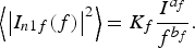 $$\left\langle {{{\left \vert {{I_{n1f}}(f)} \right \vert} ^2}} \right\rangle = {K_f}\displaystyle{{{I^{{a_f}}}} \over {{f^{{b_f}}}}}.$$
Burst noise: related to generation-recombination within semiconductor bulk [Reference Sato12]. It can be represented by an equation in the form of (2) depending on dc current (I) and a set of device-dependent parameters (f c, ab, bb, Kb), usually having a Lorentzian shape (b b ~ 2):
 $$\left\langle {{{\left \vert {{I_{nb}}(f)} \right \vert} ^2}} \right\rangle = {K_b}\displaystyle{{{I^{{a_b}}}} \over {1 + {{(f/{f_c})}^{{b_b}}}}}.$$
Thermal noise: due to thermal energy of the electrons flowing through the series resistance of the diode R S. It depends on temperature T with Boltzmann's Constant K as the proportionality factor.
 $$\left\langle {\left \vert {I_{nRs}^{} {{(f)}^2}} \right \vert} \right\rangle = \displaystyle{{4KT} \over {{R_S}}}.$$
Shot noise: due to randomness of current flowing through any semiconductor [Reference Van Der Ziel11]. Depends on electron charge q, saturation current I sat and diode current I diode.
 $$\left\langle {{{\left \vert {{I_{nshot}}(f)} \right \vert} ^2}} \right\rangle = 2q\left( {{I_{diode}} + 2{I_{sat}}} \right).$$
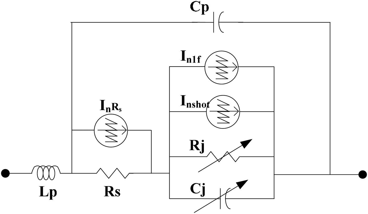
Current dependence in flicker, burst, and shot noise is conventionally assumed to be on the dc current of the device, considered as the mean current. LF noise in the Schottky diodes under study could be appropriately explained by a model dominated by flicker noise, shot noise, and thermal noise, without a burst contribution. Therefore, the topology of the noise current sources chosen was as shown in Fig. 1 with three noise current sources associated with flicker, shot, and R s thermal noise.
Noise sources in the Schottky diode circuit model.

III. SCHOTTKY DIODE IN MM-WAVE DETECTOR
To design a detector with a Schottky diode, a RF input matching network, a dc return path, and an output RF short-circuit stub plus lowpass RC output filter must be added to the diode. The microwave detector design presented in [Reference Cano, Aja, Villa, De la Fuente and Artal13] and fabricated in microstrip technology with HSCH 9161 or MZB 9161 Schottky diode models (depending on availability) was used as a platform for comparisons of LF noise measurements and simulations.
A basic simplified scheme of a Schottky diode-based Microwave detector (Fig. 2) will be used to discuss the relationship between the main function of the detector and its capability to convert LF noise. The study of the detector restricted to a resistive nonlinearity is a classical premise [Reference Middleton2] for an analytical treatment, whose validity and limitations can be later verified in simulation including nonlinear capacitances. The goal of this simplified analytic development is just to establish a draft preliminary vision of the expected detector outputs for different harmonic and noisy inputs. For example, it will be shown that ideally no down-converted PHN is expected from a quadratic nonlinearity. Nevertheless, full simulations presented later in this article, including nonlinear capacitance and an exponential diode curve model, show the limitations of this preliminary approximation, even maintaining the basic detector behavior. For example, they may affect the form of unexpected harmonic content, unexpected conversion of phase modulated (PM) noise and changes in the detector's sensitivity, depending on the type or RF signal (single or multitone, broadband, etc.). The use of Volterra series could provide a more accurate analytic description [Reference Bedrosian and Rice9, Reference Gomes, Testera, Carvalho, Fernández-Barciela and Remley10].
Simplified schema of diode-based detector.
The I–V characteristics of a Schottky diode can be expressed as (5) where n is the ideality factor and α is defined as q/nKT (where q is the electron charge, n is the ideality factor, K is Boltzmann's Constant and T is the absolute temperature in Kelvin).
 $$I = {I_{sat}}({e^{\displaystyle{q \over {nKT}}(V - I{R_s})}} - 1) = {I_{sat}}({e^{\alpha (V - I{R_s})}} - 1).$$
If a dc bias point voltage V b is assumed, the diode current can be expressed as a Taylor series for voltage values V around V b.
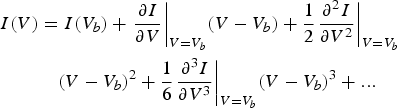 $$\eqalign{I(V) & = I({V_b}) + {\left. {\displaystyle{{\partial I} \over {\partial V}}} \right \vert _{V = {V_b}}}(V - {V_b}) + \displaystyle{1 \over 2}{\left. {\displaystyle{{{\partial ^2}I} \over {\partial {V^2}}}} \right \vert _{V = {V_b}}} \cr & \quad {(V - {V_b})^2} + \displaystyle{1 \over 6}{\left. {\displaystyle{{{\partial ^3}I} \over {\partial {V^3}}}} \right \vert _{V = {V_b}}}{(V - {V_b})^3} +...} $$
Based on the simplified schema in Fig. 2, the expression for V out will be obtained for different scenarios, depending on the type of signal applied.
According to (6) and to Fig. 2, defining v ac = V − V b and assuming a second-order truncation of the Taylor series, the output voltage of the detector before considering the RF short effect will be:
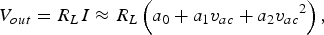 $${V_{out}} = {R_L}I \approx {R_L}\left( {{a_0} + {a_1}{v_{ac}} + {a_2}{v_{ac}}^2} \right),$$
where
 $$\eqalign{&{v_{ac}} = V - {V_b},\quad {\rm} {a_0} = I({V_b}),\quad {a_1} = {\left. {\displaystyle{{\partial I} \over {\partial V}}} \right \vert _{{V_b}}}, \cr & \quad {a_2} = \displaystyle{1 \over 2}{\left. {\displaystyle{{{\partial ^2}I} \over {\partial {V^2}}}} \right \vert _{{V_b}}}}.$$
Four basic cases will be considered:
(1) Single-tone RF input: v ac = Acosωt.
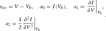
If a lowpass filtering (LPF) is applied to V out the resulting output signal will be:
 $${V_{out}}(LPF) \simeq {R_L}\left( {{a_0} + {a_2}\displaystyle{{{A^2}} \over 2}} \right) = {R_L}{a_0} + {a_2}{R_L}{R_{in}}{P_{inav}}, $$
where P inav is the available input power supposing matched input. This case represents the basic operation of a detector, providing a dc output voltage proportional to RF input power. (9) means that the slope V out(LPF) versus P inav is proportional to a2.
(2) White-noise input (filtered in a fixed RF bandwidth BW RF around ω, with BW RF ≪ ω).
A bandpass-filtered white-noise can be represented using phase and quadrature components: v ac = n i(t)cosωt - n q(t)sinωt.
Substituting into (7) and applying LPF with bandwidth BW RF/2.
 $$\left\langle {{V_{out}}(LPF)(t)} \right\rangle \simeq {R_L}{a_0} + {R_L}{a_2}\left\langle {{v_{ac}}(t)_{}^2} \right\rangle, $$
where the processes n i(t) and n q(t) are uncorrelated and 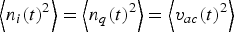 $\left\langle {{n_i}(t)_{}^2} \right\rangle = \left\langle {{n_q}(t)_{}^2} \right\rangle = \left\langle {{v_{ac}}(t)_{}^2} \right\rangle $, since they correspond to a bandpass-filtered white-noise signal. The spectrum corresponding to n i(t) and n q(t) is flat in a bandwidth BW RF/2. As they are squared, the bandwidth is doubled to BW RF. There is a down-conversion of noise from the RF bandwidth to low frequencies. LPF becomes quite relevant because with a LF bandwidth BW LF < BW RF, the output would provide an integrated version of (10) equivalent to averaging. In fact, the ratio BW LF/BW RF determines the sensitivity of the detector in radiometric applications. The average value 〈v ac(t)2〉/2 = ηBW RF corresponds to the power of the bandpass-filtered input white-noise with spectral density η in the positive frequency region.
(3) Phase modulated single-tone RF input v ac = Acos (ωt + ϕ(t)) substituted into (7) gives (11):
(11) $$ \hskip-14pt {V_{out}}(t) \simeq {R_L}\left( \matrix{{a_0} + {a_1}A\cos (\omega t + \phi (t)) + {a_2}{A^2} \hfill \cr \quad \displaystyle{{1 + \cos 2\omega t\cos 2\phi (t) - \sin 2\omega t\sin 2\phi (t)} \over 2} \hfill} \right).$$
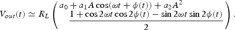
Assuming slow variations of ϕ(t) compared with ω, all the spectral components lie around ω and 2ω. Therefore, once LPF is applied:
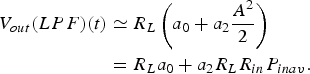 $$\eqalign{{V_{out}}(LPF)(t) & \simeq {R_L}\left( {{a_0} + {a_2}\displaystyle{{{A^2}} \over 2}} \right) \cr & = {R_L}{a_0} + {a_2}{R_L}{R_{in}}{P_{inav}}.}$$
This result is equivalent to the first case. Taking into account that a tone with only PHN behaves as a phase-modulated tone, no down-conversion of PHN should be expected from a quadratic detector.
(4) AM input: the case of double sideband (DSB) AM modulation and the cases of single sideband (SSB) plus carrier AM modulation will be distinguished:
(a). AM input tone v ac = A(t)cosωt.
Supposing a slow-varying modulating signal A(t) with null mean value and a maximum frequency = ½ BW RF and ≤BW LF, the lowpass filtered output would be:
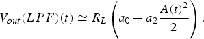 $${V_{out}}(LPF)(t) \simeq {R_L}\left( {{a_0} + {a_2}\displaystyle{{A{{(t)}^2}} \over 2}} \right). $$
A 2(t) will be the down-converted signal around the dc output with double the bandwidth of A(t), i.e. BW RF. If BW LF < BW RF, the output will provide an average power of the input envelope.
(b). If we consider two tones: SSB AM-modulated by a tone signal plus carrier:
$${v_{ac}} = {A_c}\cos {\omega _c}t + {A_m}\cos ({\omega _c} + {\omega _m})t$$

The lowpass-filtered output signal will be (14):
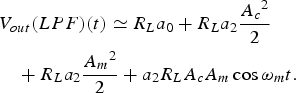 $$\eqalign{& {V_{out}}(LPF)(t) \simeq {R_L}{a_0} + {R_L}{a_2}\displaystyle{{{A_c}^2} \over 2} \cr & \quad + {R_L}{a_2}\displaystyle{{{A_m}^2} \over 2} + {a_2}{R_L}{A_c}{A_m}\cos {\omega _m}t.} $$
The first three terms correspond to: the dc offset, a dc term proportional to the carrier power, and the other dc term proportional to sideband power. The fourth term represents a down-conversion from the sideband of an AM input to the output LF noise, which is proportional to a 2. If ω m < BW LF, a spectral line around dc will appear at ω m. Note that, in this case, there is down-conversion of the modulating tone, in fact, the detector may act as a demodulator. This does not happen in case 4 (a).
With the most basic operation of a mm-wave detector, with a 50 Ω room temperature resistor loading the input, the expected output signal would contain:
(1) Dc component proportional to RF power, in this case thermal white-noise from the 50 Ω resistor in the RF bandwidth, depending on the output filter bandwidth BW LF.
(2) LF noise linearly transferred from diode noise sources (flicker, thermal, shot, etc.).
(3) Thermal noise due to dissipative losses in input and output networks.
(4) LF noise nonlinearly converted from diode sources (flicker, thermal, shot, etc.) due to the quadratic characteristics of the diode.
If a RF tone with fixed power and a given phase and amplitude noise is applied, the following components would be expected at the output:
(1) Dc component proportional to RF power of the tone plus thermal white-noise from the RF generator resistor in the RF bandwidth, depending on the output filter bandwidth BW LF.
(2) LF noise linearly transferred from diode noise sources (flicker, thermal, shot, etc.).
(3) LF noise from down-conversion only of the tone amplitude noise, not from phase noise.
(4) Thermal noise due to dissipative losses in input and output networks
(5) LF noise nonlinearly converted from diode noise sources (flicker, thermal, shot, etc.) due to the quadratic characteristics of the diode.
Note that no down-conversion is expected from PHN in a quadratic detector, according to (12).
If the RF tone is completely AM-modulated at a given modulating frequency (ω m), the demodulated ω m tone would also be expected at the output.
Prior to LF noise simulations, the ordinary mode of operation of the detector was tested in measurements and simulations. HB simulations of dc output voltage versus RF input power of the detector were compared with measurements for a 31 GHz CW tone prior to further simulations of LF noise conversion. Results are shown in Fig. 3 where it can be seen that the dc output voltage range is well predicted by the model (based on diode I–V curves and scattering parameters), but it fails to predict the compression of the voltage versus input power slope. It is beyond our scope to go deeper into these discrepancies, but as has been shown in (9)–(14), this must be kept in mind later when evaluating and comparing LF AM noise conversion in measurements and simulations.
Dc output voltage versus RF input power at 31 GHz CW input tone.
IV. SIMULATION TOOLS AND PSEUDO-ANALYTICAL PROCEDURES
Basic operation of the detector, providing a dc voltage proportional to the RF input power is simulated by HB. The result of this simulation provides the reference operating point for linearizing the circuit, assuming that noise sources will behave as small signals around that point.
Different noise analyses are possible [14], however, in this case, we consider the most suitable to be the mixer mode, i.e. as a conversion matrix problem. The models of the different noise contributions consist of stationary sources describing the spectral densities with a set of parameters corresponding to the type of noise (1), (2), (3), and (4).
Some concerns were found in the HB-based mixing-mode noise analysis applied to the detector:
– Noise models dependent on dc currents flowing through diodes (or transistors) would be expected to consider the zero harmonic solution of HB, not only the initial dc simulated current value. Depending on the simulator, it could be necessary to perform a HB simulation twice: the first to establish the “true” mean dc current from the zero-order harmonic, and the second to include that value as a dc current value, suitable to be used by the noise source as a controlling current.
– In general, built-in noise models are controlled by dc currents/voltages. Noise models using AC magnitudes (i.e. first harmonic current or voltage or incremental resistance) like in [Reference Graffeuil, Liman, Muraro and Llopis3], where the shot noise model depends on the diode pumping resistance, would definitely require a two-step simulation to provide these magnitudes for the conventional models as “false” dc magnitudes.
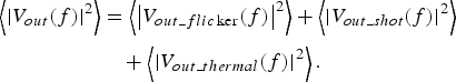
– Initially, it is not clear to the user how correlation between noise sources may affect simulation results. Noise sources are described in terms of spectral densities, but the simulator is understood to operate with voltages and currents, assuming some phases, therefore causing some ambiguity due to possible correlation. This question can be addressed by the individual simulation of each contributing noise source and then, the quadratic addition of all the contributions (15):
(15)$$\eqalign{ \left\langle {{{\left \vert {{V_{out}}(f)} \right \vert} ^2}} \right\rangle &= \left\langle {{{\left \vert {{V_{out\_flic\ker}} (f)} \right \vert} ^2}} \right\rangle + \left\langle {{{\left \vert {{V_{out\_shot}}(f)} \right \vert} ^2}} \right\rangle \cr & \quad + \left\langle {{{\left \vert {{V_{out\_thermal}}(f)} \right \vert} ^2}} \right\rangle.} $$– When a noise analysis is superimposed on an HB simulation, the noise frequency range around dc should lie within the spectrum situated between dc and the first spectral line present in the HB analysis, i.e.: if the first mixing term is placed at 1 MHz, it is not possible to obtain a noise spectrum up to 10 MHz. In this case, the noise spectrum will stop at 1 MHz.
– In the HB simulation of a mixing process, considering the carrier, if it is present, as a local oscillator (LO), and the sidebands to be RF, the existence of a large difference between power levels of both signals may cause a sort of numerical noise floor in the intermediate frequency (IF) output due to the limits of simulation's relative tolerances. To overcome this problem, an up-scaling of the minimum input power values is required; later output levels being corrected in the same ratio. Up-scaling involves some inaccuracy because the simulated levels of the weak signal are not the real ones, but it is considered to be more suitable than overestimation due to the numerical noise floor. In the cases where the level of the signal covers a wide range, the problem of numerical noise floor becomes evident below a certain threshold. Some examples will be shown later. In a large-signal HB simulation there are two possibilities: the simulation can be performed in full large-signal HB mode or the small-signal approach may be applied. The latter option may reduce the problem of the numerical noise floor.
A) Pseudo-analytical procedure
A pseudo-analytical procedure is proposed to validate direct simulator noise results, by obtaining the transfer functions in a stationary case placing conventional current sources in the position of noise current sources inside the diode and evaluating the linear transfer to the output of the detector circuit. As it was mentioned, in large-signal HB simulation there are two possibilities: the small-signal approach may be applied or the simulation can be performed in full large-signal HB mode. In the latter case, the small-signal amplitude has to be chosen to be effectively small, but above the numerical noise fixed by the simulation tolerance in voltages and currents. Note that in the diode circuit model (Fig. 1), the R S thermal noise source and flicker and shot sources are located in different positions, so it is necessary to calculate two different impedance transfer functions: Z (referred to a virtual current source I n placed in the position of flicker and shot noise sources) and Z Rs (referred to a virtual current source placed in the position R S) (16) and (17).
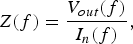 $$Z(f) = \displaystyle{{{V_{out}}(f)} \over {{I_n}(f)}},$$
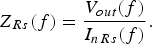 $${Z_{Rs}}(f) = \displaystyle{{{V_{out}}(f)} \over {{I_n}_{Rs} (f)}}. $$
This noise transfer function is strongly dependent on the diode bias point, as it can be seen in Fig. 4, it being higher when lower dc currents pass through the diode. However, the noise current to be transferred to the output is proportional to dc bias, the final budget being that the overall output noise is mainly proportional to bias current.
Transfer function (impedance in magnitude) between a current source in the position of the noise sources and the detector output voltage.
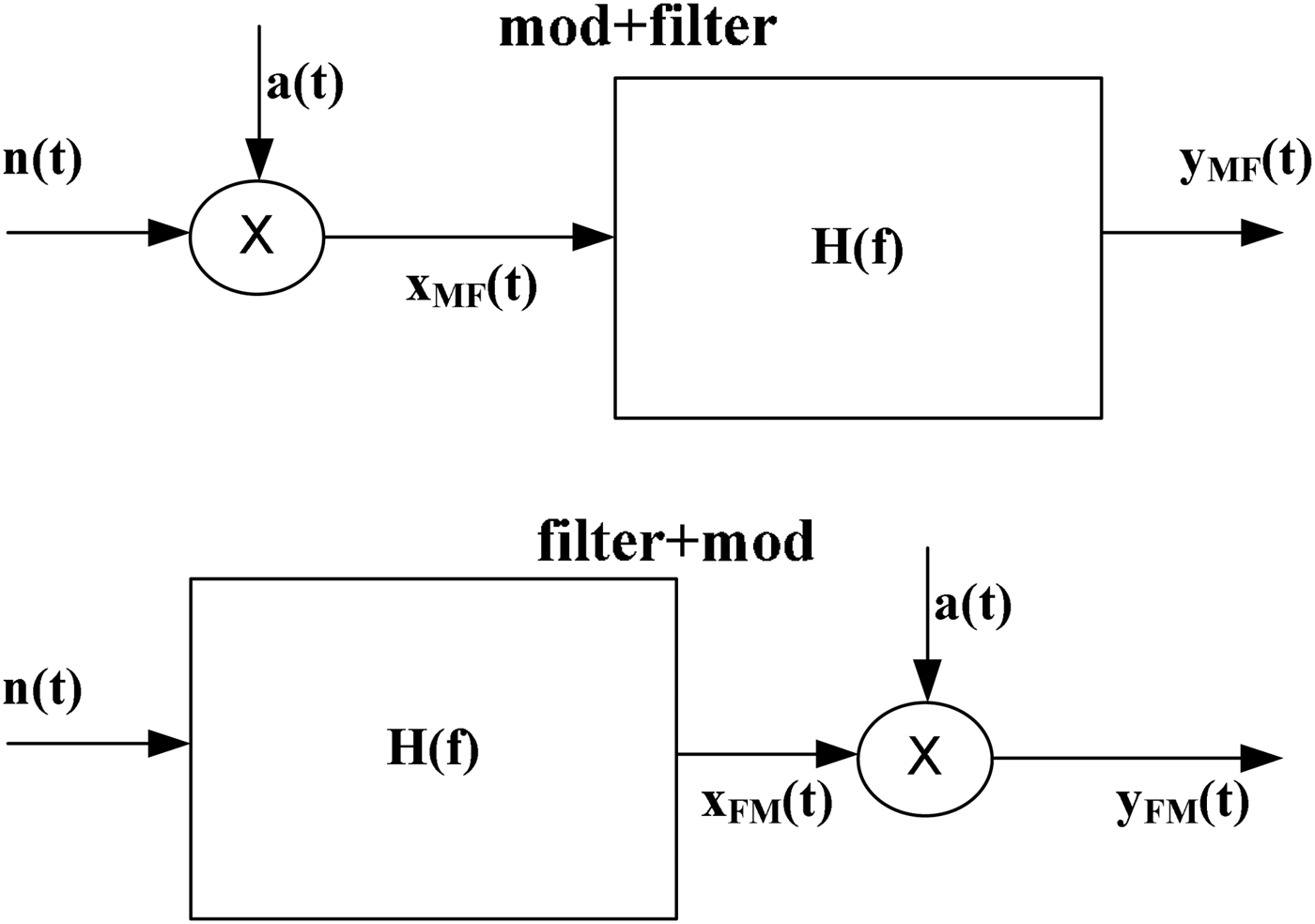
If the bias point varies periodically, the transfer function becomes time-varying, requiring the treatment proposed in [Reference Ngoya8], which generalizes the two approaches shown in Fig. 5, where n(t) is the white-noise and a(t) is the modulating signal, and it is described as noise first modulated and then filtered (MF) or noise first filtered and then modulated (FM) [Reference Conte, Bertazzi, Guerrieri, Bonani and Ghione6].
Two system approaches for the modeling of a cyclostationary noise: noise first modulated and then filtered and noise first filtered and then modulated.
The pseudo-analytical process can be extended from the stationary case to the cyclostationary case and the transfer functions can also be obtained including the cyclostationary sources in the HB simulation.
When RF signals are present in the circuit, two cases can be distinguished:
(1) RF frequency much higher than noise frequencies and absence of low-frequency (LF) signals.
(2) RF plus LF signal (i.e.: RF modulated by LF) with LF in the range of noise frequencies.
The first case could still be considered as a stationary case from the point of view of currents governing diode noise sources. The difference would be that the dc value should take into account the dc contribution from rectified RF in the diode, not only the dc values of the initial default dc simulation without RF pumping.
The second case would be that of a RF tone AM-modulated by an envelope or just a RF tone with some amplitude noise. In this case, the LF signal may fall in the output noise spectrum of interest. Two different sources of output noise can be distinguished: diode noise sources under cyclostationary regime and RF noise down-conversion.
For shot noise, [Reference Graffeuil, Liman, Muraro and Llopis3] proposes the evaluation of a small-signal dynamic resistance of the pumped diode, measured simultaneously with the noise, not necessarily equal to the differential resistance obtained from the I–V dc characteristics. Our attempts to obtain this by simulation show differences with the differential resistance depending on the range of small-signal amplitudes. Later we will propose a second-order Taylor approach to obtain this analytically. In our initial modeling we will use the approach evaluating the new dc quiescent point under RF and/or under RF + LF pumping for flicker noise (1), and also for shot noise (2).
Note that for analysis purposes, the influence of the cyclostationary case will be present both in the noise source values (procedure to simulate the average current controlling the noise sources), and in the transfer function from noise sources to the output. Moreover, for comparisons with HB noise simulations, it should be taken into account that the simulated noise spectrum cannot overlap the lowest HB frequency mixing terms.
Down-converted RF noise may lie in the frequency range of LF noise. To evaluate RF noise down-conversion, a small-signal sideband source at a given offset frequency f m (ω m = 2πf m) with respect to the carrier (ω c = 2πf c) is placed at the input, and the output voltage at f m is obtained considering contributions from both, upper (H u) and lower (H d) sidebands (18).
 $$\eqalign{& {H_u}({f_m}) = \displaystyle{{{V_{out}}({f_m})} \over {{V_{sb}}({f_c} + {f_m})}} \cr & {H_d}({f_m}) = \displaystyle{{{V_{out}}({f_m})} \over {{V_{sb}}( - {f_c} + {f_m})}} = \displaystyle{{{V_{out}}({f_m})} \over {{V_{sb}}{{({f_c} - {f_m})}^{\ast}}}}.} $$
Once the transfer functions are available, the following calculations are done:
 $${\left\langle {{{\left \vert {{I_n}({f_m})} \right \vert} ^2}} \right\rangle = \left\langle {{{\left \vert {{I_{flic\ker}} ({f_m})} \right \vert} ^2}} \right\rangle + \left\langle {{{\left \vert {{I_{shot}}({f_m})} \right \vert} ^2}} \right\rangle},$$
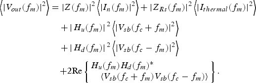 $$\eqalign{\left\langle {{{\left \vert {{V_{out}}({f_m})} \right \vert} ^2}} \right\rangle &= {\left \vert {Z({f_m})} \right \vert ^2}\left\langle {{{\left \vert {{I_n}({f_m})} \right \vert} ^2}} \right\rangle + {\left \vert {{Z_{Rs}}({f_m})} \right \vert ^2}\left\langle {{{\left \vert {{I_{thermal}}({f_m})} \right \vert} ^2}} \right\rangle \cr & \quad + {\left \vert {\left. {{H_u}({f_m})} \right \vert} \right.^2}\left\langle {{{\left \vert {{V_{sb}}({f_c} + {f_m})} \right \vert} ^2}} \right\rangle \cr & \quad + {\left \vert {\left. {{H_d}({f_m})} \right \vert} \right.^2}\left\langle {{{\left \vert {{V_{sb}}({f_c} - {f_m})} \right \vert} ^2}} \right\rangle \cr & \quad\, {\rm + 2 Re}\left\{ \matrix{{H_u}({f_m}){H_d}{({f_m})^{\ast}} \hfill \cr \quad \left\langle {{V_{sb}}({f_c} + {f_m}){V_{sb}}({f_c} - {f_m})} \right\rangle \hfill} \right\}.} $$
According to (12), no down-conversion of PHN is expected when a phase-noisy RF tone is applied to a quadratic nonlinearity. In (20) phase modulation and quadratic nonlinearity means that the fifth-order term would cancel the addition of the third- and fourth-order terms (21).
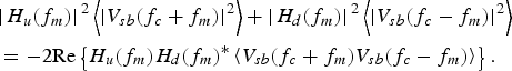 $$\eqalign{& {\left \vert {\left. {{H_u}({f_m})} \right \vert} \right.^2}\left\langle {{{\left \vert {{V_{sb}}({f_c} + {f_m})} \right \vert} ^2}} \right\rangle + {\left \vert {\left. {{H_d}({f_m})} \right \vert} \right.^2}\left\langle {{{\left \vert {{V_{sb}}({f_c} - {f_m})} \right \vert} ^2}} \right\rangle \cr & = {\rm - 2 Re}\left\{ {{H_u}({f_m}){H_d}{{({f_m})}^{\ast}}\left\langle {{V_{sb}}({f_c} + {f_m}){V_{sb}}({f_c} - {f_m})} \right\rangle} \right\}.} $$
For example, with a signal v ac = Acos (ωt + ϕ(t)), corresponding to a PM carrier modulated by a sine function with a low modulation index, it can be verified that V sb(f c + f m) = −V sb(−f c + f m). The phase shift in the lower sideband causes a cancellation after the detection which would not happen if sidebands corresponding to an AM-modulated carrier were applied to the same pair of transfer functions H u and H d.
Eventually, in a more realistic circuit with a not-only-quadratic nonlinearity and in the presence of other signals, it could be of interest to evaluate PHN down-conversion.
Additionally, even the case of frequency doubling of the offset sidebands (considering the quadratic nature or the detector) could be evaluated for AM or PM sidebands:
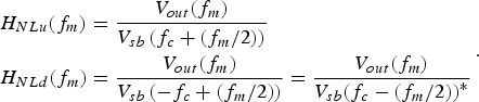 $$\eqalign{& {H_{NLu}}({f_m}) = \displaystyle{{{V_{out}}({f_m})} \over {{V_{sb}}\left( {{f_c} + ({f_m}/2)} \right)}}\cr &{H_{NLd}}({f_m}) = \displaystyle{{{V_{out}}({f_m})} \over {{V_{sb}}\left( { - {f_c} + ({f_m}/2)} \right)}} = \displaystyle{{{V_{out}}({f_m})} \over {{V_{sb}}{{\left( {{f_c} - ({f_m}/2)} \right)}^{\ast}}}}}. $$
The additional terms due to (22) could be added to (20). It provides a tool to consider quadratic transformations of the noise sidebands from fm/2 to fm, and even it can be extended to take into account other kinds of nonlinearities. Nevertheless, in practice, this contribution was not found relevant.
B) Pseudo-analytical results
When the detector is dc biased, in the absence of a RF tone at the input, there is good agreement between the pseudo-analytical procedure and the simulator, as it can be seen in Fig. 6 for 0.4 mA bias current, where the separate contribution of flicker noise has also been represented. The question of correlation between sources has been analyzed in this case: the simulation of the completely biased detector was done, first considering separately contributions of shot noise, flicker noise, thermal noise, and then adding quadratically all those quantities (15). On the other hand, all the noise sources were included together in a single simulation. Results show almost no difference, so the results of the complete simulation with all the noise sources activated could be considered as valid.
Comparison between results simulated with a built-in procedure (labelled “simul”) and pseudo-analytically calculated results (labelled “func_trans_tot”). Flicker noise contribution is plotted separately (labelled “func_trans_only_flick”).
With the presence of a RF tone at the input of a detector, two cases should be considered to obtain the complete output signal: conversion of AM sidebands and possible conversion of PHN bands.
C) AM sideband conversion: transfer function obtained for an input tone with flat AM sidebands in HB
If the carrier contains AM noise in the form of sidebands, conversion to the output is produced as could be expected from (14). The output levels are proportional to the sideband levels.
Transfer functions defined by (18) and (21) relate (see Fig. 2) V out(f m) and V in(f c ± f m), but those voltages are applied at different impedances and the ratio of impedances should be taken into account to operate with power spectral densities (PSD):
 $${P_{outdBm/Hz}} = {P_{insbdBm/Hz}} + {H_{dB}} + 10\log ({R_{in}}/{R_{load}})$$
Where P insb represents the input PSD corresponding to V in(f c ± f m), P out the power spectral density corresponding to V out(f m) and H dB the combined transfer function. For R in = 50 Ω (assuming input matched) and R load = 1 MΩ the correction term is −43 dB.
Normal operation power levels at the input of the detector may be around −30 dBm, nevertheless, a 9.5 dBm RF tone at 33 GHz is applied at the input of the detector to cause some dc rectification in the diode. A certain arbitrary level of flat-frequency AM noise is superimposed to see its conversion at the output. When the level of this AM noise is varied, the problem of the numerical noise floor arises. It has been found that with a main tone of 9.5 dBm at 33 GHz, the level of the sidebands should be at least around −30/−20 dBm to find correspondence of linear increments between input and output (see Fig. 7). Note the coincidence of small-signal HB results with large-signal HB results in the linear range.
Determination of numerical noise floor in HB sideband conversion simulations in the presence of a 9.5 dBm carrier at 33 GHz when sideband power input is swept (P sbin). Comparison of small-signal and large-signal HB simulations showing coincidence in the linear range of large signal HB.
Therefore, it becomes necessary to downscale simulated results with an input level where the simulated response is linear (−20 dBm) to a more realistic lower level (i.e. −120 dBm). Results are shown in Fig. 8, including the overestimated simulated results for −120 dBm. Note the great difference between power spectral densities simulated and downscaled at −120 dBm.
The transfer function computed and validated in the linear range in Fig. 7 (−20 dBm) is used to compute response with a sideband level below the linear range (−120 dBm). Notice in this case the difference between the simulated result and the corrected-downscaled result.
D) PM sideband conversion: transfer function obtained for an input tone with PM sidebands in HB
According to (12), down-converted PHN in an ideal quadratic detector should be null. To verify this, an ideal quadratic nonlinearity (a 0 = a 1 = 0 in (7)) was used as an ideal reference simulation workbench. An RF tone with different RF power levels and with or without PHN was applied. In agreement with (12), the output noise of the ideal detector is the same and practically null and flat in both cases, showing no influence of the RF generator phase noise.
Nevertheless, when we consider the complete detector circuit (including all the elements described with their corresponding models, particularly the diode nonlinearity, not only quadratic, resistors, and distributed parts), in the presence of a RF tone, discrepancies may arise between simulation results and theory for the ideal case. Moreover, the application of the pseudo-analytical procedure may provide different results if the numerical noise floor is not taken into account.
Using (18), the corresponding transfer function obtained with a HB of the mixing process, considering carrier and out-of-phase sideband pairs of tones (PM by a sine with a low modulation index), was used to calculate the noise at the output of the detector when a 9.5 dBm signal with a certain level of PHN was applied at the input. The detector is not dc biased, except for its own rectification of the RF tone. Results are compared with the ones provided by the built–in HB noise simulation in Fig. 9. Sideband power level was swept to find the optimum value to provide linear range, but the built-in procedure shows some numerical noise floor which we tried to avoid using the transfer function procedure. It should be mentioned that the input PHN level has a large variation range, contrary to the case of the flat amplitude noise level used in simulations in Fig. 8.
Noise output voltage converted from RF input PHN of a 9.5 dBm tone, estimated by built-in simulator procedure and by pseudo analytical transfer function (HB mixing).
For a better understanding of the problem, the built–in HB noise simulation procedure was applied to simulations with different flat noise levels of PHN in the input signal, in order to obtain an alternative transfer function for later application to the same input PHN level as in Fig. 9. Results are shown in Fig. 10, showing the same trend as the transfer function obtained with the HB mix. Therefore, we conclude that the numerical noise floor associated with the lower noise levels corresponding to the highest offset frequencies is responsible for that discrepancy.
Noise output voltage converted from RF input PHN estimated by built-in simulator procedure (labelled “psd out actual”) and by pseudo analytical transfer function obtained by using built-in noise simulation with two different flat levels: −20 and −90 dBm.
V. Setup for stand-alone diode and detector power spectral density characterization in dc regime
The following setup (Fig. 11) inspired in [Reference Hardy, Deen and Murowinski15] was used to obtain the power spectral density of both the stand-alone diode and a complete detector using model MZB-9161 (as model HSCH-9161 was no longer available at that time). In [Reference Grop and Rubiola16], a more complex scheme is proposed to de-embed the noise contribution of a single detector in a system containing three detectors.
Setup for noise measurements of Schottky diode (input upper connection) or detector (input down connection).
Comparisons between measurements and simulations are made in terms of noise power spectral density at the signal analyzer input. The measurement system noise floor is modeled and included in the simulations together with known contributions of noise added by several resistors (including input and output impedances, and biasing resistors), prior to comparison with the measurements (see scheme in Fig. 11). In this case, comparisons are made with true measured magnitudes, modeling additional noise sources, but without de-embedding them to obtain the intrinsic noise sources of the diode. We chose to avoid mixing modeled sources and measurements, providing not only the model of the diode noise sources but also a model of the complete setup.
Biasing is applied to the diode through a 1 Hz lowpass filter built using a RC chain ladder. Biasing voltage is obtained from batteries with a high-quality stabilized resistance voltage divider. The output noise frequency range was chosen between 1 Hz and 100 KHz, where the effect of bias variation on 1/f noise was most evident against the system noise floor. Later in other setups, it was necessary to reduce the useful frequency range due to the noise floor increase.
In Fig. 11, the setup for the detector is shown (input down connection). The detector Input is loaded with a 50 Ω room-temperature load. Initially the RF input generator is turned-off. Calculations to compute noise in the circuit in Fig. 11 (upper part) are slightly modified to include 50 Ω input resistance and detector resistance contributions.
The first step to establish the noise floor of the measurement system (see circuit in Fig. 11 and fitted measurements in Fig. 12) is to short-circuit the input of the instrumentation amplifier and to measure the output noise with the same gain settings used in the measurements. This is the most intuitive approach. For a deeper study additional impedances such as open circuit and an equivalent resistance could be placed at the input to compare.
Measurement system noise floor (with instrumentation amplifier short-circuited input): measured values and fitted to a model.
Once the noise floor is modeled, the detector output is connected to the Stanford amplifier, placing a room-temperature 50 Ω resistor at the detector input, obtaining the power spectral density measurements at V out on a 1 MΩ resistor, then fitted to the model of (1). The optimum set of parameters to fit measurements in Fig. 13 is K f = 1.6 × 10⁻³, a f = 3.3790, b f = 1.3008. The current I in (1) is the nominal dc diode current. These parameters will be initially fixed for the simulations including RF and LF signals in the next section.
Output detector noise under different dc bias points measured and fitted to the model in HB-based LF noise simulation.
VI. SETUP FOR DETECTOR POWER SPECTRAL DENSITY CHARACTERIZATION IN RF AND CYCLOSTATIONARY REGIME
Inherent decoupling of RF input–dc output in the detector was used to apply a LF modulating signal through the RF input to the diode (controlling its intrinsic noise sources) in the same frequency range evaluated at the output or higher. Three possible detector inputs were considered: RF turn off, CW RF (non-modulated), RF AM-modulated by several modulating frequencies (f m): 50, 100, 500 KHz, and 1 MHz. Note that 50 and 100 KHz fall into the output noise frequency range of measurements. The RF input signal was previously visualized in a spectrum analyzer to evaluate PHN plus AM noise and AM sidebands, to be later taken into account for the simulations.
RF input power level was fixed at 9.5 dBm to produce a significant rectifying current and the corresponding LF output noise. The detector design is not intended for this RF input level beyond the quadratic zone, but we are mainly focused on the problem of noise prediction under forced regimes. Detector output noise for RF input levels around −30 dBm (quadratic zone) did not stand out without bias. To verify this, the output noise power spectral density of the detector was measured with −30 dBm input power at 33 GHz and with −20 dBm input power at 33 GHz with the diode unbiased and biased with 0.1 mA (Fig. 14). The increment from −30 to −20 dBm was not relevant in the 1/f frequency range of measured output noise, but the change from no dc bias to 0.1 mA was quite noticeable. Therefore, a higher level of input power was applied, namely 9.5 dBm, which was able to cause some rectifying in the diode and the consequent increase in 1/f LF output noise.
Output noise power spectral density for −30 and −20 dBm input tone with detector unbiased and biased with 0.1 mA current. Note that the main influence is due to bias current not to the increment in RF power.
As it was mentioned, additional dc bias as well as diode rectification was applied to study dependence of noise sources on dc current under cyclostationary regime. For the simulations, dependence of the noise sources on the simulated dc current, on the “true” HB mean current (harmonic #0), on the LF current component and on the first harmonic current were computed, choosing dependence on the “true” mean current as it was closer to measurements and was more feasible in agreement with theory. Initially AM/ PHN conversion to quasi-dc was not taken into account. Then, it was considered using the linearized transfer functions previously discussed and simulator built-in conversion.
To evaluate different simulations of down-conversion noise contributions, the case of un-modulated RF input is chosen as starting point which mostly coincides with the system noise floor (Fig. 12).
Note that when the RF generator is turned on (Fig. 15), flat noise level increases by about 10 dB. This increase can be attributed to shot noise due to the additional rectified dc current, some contribution from converted amplitude noise and maybe converted phase noise. Measurements are plotted along with several simulations in Fig. 16: the LF noise simulation; including all contributions (shot, flicker, thermal) controlled by rectified current except for converted noise; including converted noise using a linearized transfer function as defined in (18) (flat AM noise); including converted noise using a linearized transfer function as defined in (21) (PHN) and including converted PHN using simulator built-in procedure. An additional trace is composed to provide the best fit with measurements, requiring the combination of LF contributions from diode plus AM noise down-conversion and PHN down-conversion weighted with a voltage factor (around 0.0125). The weighting factor combined with an arbitrarily chosen AM level provides a quite reasonable fit with the level of noise at the output of the detector. The need for a weighting factor <1 indicates an overestimation of conversion which could be related to the difference in slope in Fig. 3. Nevertheless, this contribution is necessary to provide the particular shape measured between 1 and 10 KHz.
Detector output power spectral density with a 9.5 dBm at 33 GHz input signal: Measurements and simulations considering only flicker, shot, and thermal noise of the diode and the detector circuit under rectified current, adding flat AM noise down-conversion, adding PHN down-conversion computed with a transfer function and with the built-in procedure, and finally adding a combination of converted flat AM noise and converted PHN with a weighting factor to provide the best fit.
Measured detector output power spectral density for the detector dc biased at 0.1 mA without RF applied, with a 9.5 dBm 33 GHz input signal and with the same carrier, but with 50 KHz AM modulation.
The next step is to bias the diode adding the current directly applied to the rectified current up to 0.1 mA. Measurements of the output power spectral density are shown in Fig. 16 for three different cases, all with the same total dc current flowing: without RF applied at the input, with a 9.5 dBm RF tone at 33 GHz and with the same RF carrier modulated with a 50 KHz tone. As we have seen previously, there is an increase in the noise level when the RF signal is turned on, even with the same dc current, including rectified plus applied dc current. Converted noise from RF input could be responsible for this increase. In the range between 100 Hz and 2 KHz there is no difference due to the addition of 50 KHz AM modulation, but in the range of 10 KHz a noise shoulder arises. The shape resembles the PHN of a phase-locked oscillator, lower inside the loop bandwidth because of the reference tracking and higher outside the loop bandwidth, similar to following a free running oscillator. In fact the RF generator used is synthesized both when it produces a single tone and when AM is generated. Of course, the demodulated 50 KHz signal appears at the output as well as its next harmonic at 100 KHz. The level difference between the modulated case and the single tone case in the range between 50 and 100 KHz could be caused by the AM noise corresponding to the sidebands, or to an increase in the shot noise due to the relatively slow-varying modulating current. In all cases, the mean dc current is the same.
Focusing first on the RF single tone case, new comparisons are made between measurements and simulations (Fig. 17). There is only a slight increase, compared with the unbiased case (Fig. 15), which simulations reveal.
Detector output power spectral density with a 9.5 dBm 33 GHz input signal and diode biased at 0.1 mA (including rectification): Measurements and simulations considering only flicker, shot, and thermal noise of the diode and the detector circuit, adding PHN down-conversion computed with the built-in procedure, and adding a combination of converted flat AM noise and converted PHN with a weighting factor to provide the best fit.
Considering that the AM-modulated carrier provides a LF cyclostationary regime for the diode when a 50 KHz modulating signal is applied to the AM input of the RF generator, biasing the diode with a total current of 0.1 mA, measurements show a change in the Lorentzian shape found in the previous measurements only with a carrier which is difficult to fit with our previous simulations. Simulated results are available only up to 50 KHz because the HB built-in noise simulation is only possible between dc and the minimum frequency present in the HB frequency base, 50 KHz in this case. Different simulation results are shown in Fig. 18, considering only LF noise sources, adding full PHN down-conversion, adding weighted PHN down-conversion and finally AM noise down-conversion. Simulations fitting the measurements are not as satisfactory as in Figs 15 and 17. In an attempt to improve this situation, different current dependences of LF shot noise sources on total dc current or on 50 KHz component current were tested, but without further improvement. Finally, the phase-locked oscillator demodulated noise is considered to be the most feasible explanation of the shape.
Detector output power spectral density with 9.5 dBm 33 GHz, 50 KHz modulation, and diode biased at 0.1 mA (including rectification): measurements and simulations considering only flicker, shot and thermal noise of the diode and the detector circuit, adding PHN down-conversion computed with the built-in procedure, and adding a combination of converted flat AM noise and converted PHN with a weighting factor to provide the best fit.
For the sake of clarity, simulations including biased diode noise and converted noise from a RF tone, modulated or not and which achieve the best fit are superimposed with measurements in Fig. 19.
Detector Output power spectral density with 9.5 dBm 33 GHz, diode biased at 0.1 mA (including rectification) and 50 KHz modulated or not: Measurements and simulations considering flicker, shot and thermal noise of the diode and the detector circuit, adding a combination of flat converted AM noise and converted PHN with a weighting factor to provide the best fit.
VII. DIFFERENTIAL SETUP FOR DETECTOR POWER SPECTRAL DENSITY CHARACTERIZATION IN RF AND CYCLOSTATIONARY REGIME
The previous section showed how AM (and possibly PM) noise of the RF signal applied to the detector is a source of uncertainty which requires a weighting factor to fit the measured detector output noise. To avoid, or at least, reduce this problem by cancellation, a simple differential configuration similar to [Reference Graffeuil, Liman, Muraro and Llopis3], but implemented in mm-wave technology, is tested utilizing both inputs of the instrumentation-low-noise-amplifier in differential mode, subtracting the outputs of two detectors fed by the same RF generator and assuming that both detectors are equal. Some requirements needed to be fulfilled: availability of a Ka-band 3 dB coupler, availability of two detectors with the same model of diode and minimum impairment between circuits, RF paths, etc. For simplicity in this setup detectors were not biased. A scheme of a more complex setup for optimum removal of noise contributions at LFs can be found in [Reference Bedrosian and Rice9], requiring three detectors and a lock-in amplifier.
In our first assembly the unbalance of the RF-DC response between the two detectors was enough to cause an increment in output noise. To minimize the output noise a rotary attenuator and additionally two phase shifters were inserted, adjusting the power to obtain the same dc output level in both branches (Fig. 20). Contrary to simulations, in practice, phase shifters did not seem to affect results noticeably. Comparisons between measurements and simulations were made in terms of noise power spectral density at the signal analyzer input (V out in Fig. 21). The system noise floor including short-circuited cables showed a shoulder which forced us to reduce the valid range between 10 and 100 KHz, which excludes the 1/f zone, therefore, focusing this differential setup on shot noise, without external dc bias and under cyclostationary operation.
Improved setup for adjusting the operation point of both detector diodes. Scheme and photograph of the Ka-band coupler connected to the two detectors with phase shifters and an attenuator.
Measured output noise power spectral density for 0dBm per branch (3 dBm total) and 8 dBm per branch (11 dBm total) RF input power with and without adjustment for equal dc output (DC balanced). Simulations for both input powers and the measured/simulated system noise floor are superimposed (labelled NFG).
A small attenuation around 0.14 dB in the branch of the most sensitive detector is enough to achieve the minimization of output noise thanks to the dc balance of both detectors, as can be observed in Fig. 22 for a CW RF input signal of 0 dBm per detector (+3 dBm total) and for 8 dBm per detector (+11 dBm total). As can be seen in Fig. 21, dc balance reduces the initial noise measurements about 14 dB. This minimization facilitates better coincidence with the results simulated with the conventional shot noise model.
System Output power spectral density with 8 dBm per branch at 33 GHz input tone: measurements and simulations with conventional shot noise model, noise floor simulated and measured.
For the sake of clarity, comparison of measurements and simulation will be made for 8 dBm per detector RF input power in a smaller frequency range corresponding to the flat spectrum. Simulated results predict a noise level slightly higher than was measured (see Fig. 22).
In the case of a 50-KHz AM-modulated 33-GHz carrier, a pumping signal is present in a frequency in the range of the output noise frequencies of interest and suitable to cause a periodic variation of the diode bias point. We can alternatively propose a modified shot noise model according to [Reference Graffeuil, Liman, Muraro and Llopis3], depending on R dp: a dynamic resistance under pump condition, replacing (4) for (24) to compare fitting of measurements, as can be seen later in Fig. 23.
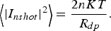 $$\left\langle {{{\left \vert {{I_{nshot}}} \right \vert} ^2}} \right\rangle = \displaystyle{{2nKT} \over {{R_{dp}}}}.$$
System Output power spectral density with 11 dBm at 33 GHz input tone (8 dBm per branch) AM-modulated by 50 KHz: noise floor measured (NF_grounded) and modelled (SIM_DIF_GND), measurements (Meas) and simulations with the conventional shot noise model (SIM_8dBm_AM) and a shot noise model based on small-signal resistance (SIM_8dBm_AM_ Rdp).
In [Reference Graffeuil, Liman, Muraro and Llopis3], R dp is measured and compared with the computed inverse of the I–V slope. An analytical approach could be considered, assuming a Taylor series (6) of the diode current (5) truncated in the second term. The resistance can be computed according to (25) with the assistance of an HB simulation test bench, showing dependence on the small-signal voltage swing. If ΔV is neglected, R dp will match the inverse of the I–V slope at the bias point and both the conventional and modified models should provide the same results.
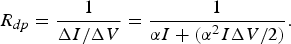 $${R_{dp}} = \displaystyle{1 \over {\Delta I/\Delta V}} = \displaystyle{1 \over {\alpha I + ({\alpha ^2}I\Delta V/2)}}. $$
Nevertheless, HB simulation enables the computation of how self-biasing fixes the operation point of the diode, therefore, R dp can also be computed by increments in a HB simulation workbench, focusing on the junction conductance. Junction capacitance current will be neglected in the estimation of R dp, obtaining a high value in the range of 5 KΩ. In this case both shot noise models fit similarly with output noise power spectral density measurements, as it can be seen in Fig. 23.
VIII. CONCLUSIONS
The capability of HB-based simulation tools to predict LF noise transference and down-conversion in diode-based detectors under different regimes has been discussed. Only in dc operation, simulations and measurements show fully satisfactory agreement. With a RF tone pumping the diode, some issues should be taken into account. Currents controlling LF noise sources should consider mean current values including rectification due to RF tones. This requires a special implementation of the simulations, because built-in procedures usually only account for initial dc current obtained in a dc simulation previous to the HB simulation.
We have found a trend to overestimate down-conversion, from AM and, possibly, PM noise, in mixer-based noise simulations and in built-in noise simulations. This trend could be related to a magnification of large-signal modeling errors when moving from conventional detector simulations to LF noise simulations, and also to disparities among input power levels, causing a sort of numerical noise floor in HB mixing simulation. The results could be meaningful, but should be weighted. The use of small-signal HB may reduce this numerical noise floor problem. An alternative pseudo-analytical procedure is proposed, but it also suffers from the aforementioned numerical noise floor. This procedure uses conversion-matrix type formulation, which relates the carrier noisy sidebands of the input signal to the detector output spectrum through a pair of transfer functions obtained in commercial software.
Measurements for comparison with simulations have been provided by a simple measurement system used to characterize, not only a single diode, but also a detector fabricated with the same model of diode. Unfortunately, when establishing proper comparisons, large LF noise dispersion was found between different units of the same diode model fabricated in different runs, and even between different manufacturers of the same diode model. In the measurement of noise, the main concern was to have a clear distinction between the device-under-test's noise and the setup noise floor, which was also modeled. Limitations of the measurement system in discriminating different contributions to output noise can be reduced with a more complex differential topology. However, in this case, the difficulties incurred in shielding caused a noise floor increase, reducing the range of meaningful measurements to the flat portion of spectra. The conventional shot noise model and a shot noise model based on small-signal resistance were also applied to fit measurements, both seeming suitable in the presence of a LF modulating signal with a limited range of power, compared with other direct LF injection setups.
ACKNOWLEDGEMENTS
The authors would like to thank the Spanish Ministry of Science and Innovation (MICINN) for the financial support provided through projects TEC2011-29264-C03-01, CONSOLIDER-INGENIO CSD2008-00068 (TERASENSE), TEC2014-58341-C4-1-R, FEDER co-funding, CONSOLIDER-INGENIO CSD2010-00064 and the University of Cantabria Industrial Doctorate programme 2014, project: “Estudio y Desarrollo de Tecnologías para Sistemas de Telecomunicación a Frecuencias Milimétricas y de Terahercios con Aplicación a Sistemas de Imaging en la Banda 90–100 GHz”. The authors would like to express their gratitude to all the staff of DICOM's Microwaves & RF group, and particularly to Ana Perez, Eva Cuerno, and Sandra Pana for their help with the fabrication of the prototypes and to Dermot Erskine for the correction of the text.
Jéssica Gutiérrez Asueta was born in Santander (Spain) in 1985. She received her Telecommunications Engineering degree and the Master degree in ‘Information Technologies and Mobile Network Communications’ from the University of Cantabria (Spain) in 2010 and 2011, respectively; and she obtained an award for her Master Thesis Project in 2011. She joined the Department of Communications Engineering (University of Cantabria) in 2010, where she has participated in some research projects, particularly in a Spanish Consortium of research in the field of ‘Terahertz Technology for Electromagnetic Sensing Applications’. Since 2014, she has been working for Erzia Technologies and is simultaneously preparing for her Ph.D. degree under a grant of the University of Cantabria for Industrial Doctorate. Her area of interest includes the design, assembling and testing of hybrid and MMIC circuits in millimeter waves, and particularly for imaging system in W-band.
Kaoutar Zeljami was born in Tetouan (Marroc) in 1984. She received her Master's degree in Electronics and Telecommunication Systems in 2008, from University Abdelmalek Essadi (Marroc). She obtained a MAEC-AECID Doctoral Grant, sponsored by Spanish Ministry of Foreign Issues, and she joined the RF and Microwaves Group of Department of Communications Engineering of University of Cantabria, Spain, in 2008. She achieved the Master's degree in Information Technologies and Mobile Networks Communications from University of Cantabria, Spain, in 2009. She worked in the project “EDA KORRIGAN” and she participated in a Spanish Consortium of research in the field of “Terahertz Technology for Electromagnetic Sensing Applications”. She obtained her Ph.D. degree from the University of Cantabria in 2012. Her area of interest includes Characterization and Modeling of Semiconductor Devices in Terahertz frequencies, particularly, Schottky Diodes.
Enrique Villa received his degree in Telecommunications Engineering, the Master's degree in Mobile Network Information and Communication Technologies and the Ph.D. degree in Mobile Network Information and Communication Technologies from the University of Cantabria in 2005, 2008 and 2014, respectively. His research activity is related to the design and performance of radio-astronomy receivers, taking special interest in cryogenic behavior of phase switches, low-noise amplifiers and detectors, and design, analysis and testing of microwave devices.
Beatriz Aja received her Telecommunications Engineering degree and the Ph.D. in 1999 and 2007, respectively, from the University of Cantabria, Spain. From 2008 to 2012 and from 2013 to 2015 she has been invited as scientist at the Fraunhofer Institute for Applied Solid State Physics (Germany), in a joint collaboration project with Centro Astronómico de Yebes (Spain). Since 1999 she has been with the Department of Communications Engineering at the University of Cantabria. Her main research interests are microwave and millimeter-wave circuits and systems design, and in particular the design of microwave low noise amplifiers.
Luisa de la Fuente graduated from the University of Cantabria, Santander, Spain in 1991 and received her Doctoral degree in Electronics Engineering in 1997. From 1992 to 1993, she was an Associate Teacher in the Department of Electronics, University of Cantabria. She is currently a lecturer in the Department of Communication Engineering, University of Cantabria. Her main research interests include design and testing of microwave circuits in both hybrid and monolithic technologies. In the last years she has worked in the projects focused in the development of radiometers for space applications, like the Planck Mission, in particular in low noise amplifiers at room and cryogenic temperatures. Currently she is involved in several projects focused on the development of very low noise receivers in the 30 and 40 GHz frequency bands for the QUIJOTE experiment, and on the development of polarimeter receivers at W band.
Sergio Sancho received his Ph.D. degree in 2002 from the Communications Engineering Department from the University of Cantabria, Spain. At present, he works at the University of Cantabria, as an Associate Professor in Communications Engineering Department. His research interests include the nonlinear analysis of microwave autonomous circuits and frequency synthesizers, including stochastic and phase-noise analysis.
Juan Pablo Pascual was born in Santander (Spain) in 1968. He received his Master's degree in Electronics with honors (1990) and the Ph.D. degree in Electronic Engineering (1996), both from the University of Cantabria, where he works currently as Associate Professor in the Communications Engineering Department, teaching Signal processing, RF, and MMIC design. His research interests are active device modeling, MMIC design methodology of nonlinear functions, and subsystems, from microwaves to millimeter waves and Terahertz, and system simulation. He has co-authored more than 60 contributions in International Journals and Congress. He has been involved in modeling and design projects with industries and research institutions from Spain and with international companies and institutions like Daimler Chrysler, OMMIC, ESA, Technical University of Darmstadt (where he stayed during 1999), the PLANCK, and the QUIJOTE mission consortiums and a Spanish Consortium of research in the field of “Terahertz Technology for Electromagnetic Sensing Applications”.


 Open access