




Introduction
Future wireless communication systems targeting applications such as virtual and augmented reality, Industry 4.0, and holography require ultra-reliable operation, energy-efficient transceivers, data rates exceeding 1 Tb/s, and end-to-end latencies below one millisecond [Reference Giordani, Polese, Mezzavilla, Rangan and Zorzi1, Reference Saad, Bennis and Chen2]. Beyond conventional communication scenarios, these stringent requirements increasingly overlap with the demands of high-resolution imaging and sensing, including short-range radar and passive imaging receivers. In such applications, wide instantaneous bandwidths, low-noise figures, and stable amplitude and group delay are essential to achieve high spatial resolution, accurate target detection, and  $ \gt $100 Gbps data rates. To meet these performance requirements, wireless systems have progressively migrated toward the D-band and (sub-)terahertz (THz) frequency regime, above 110 GHz, where large absolute bandwidths are available. Experimental demonstrations in this frequency range have already achieved data rates exceeding 100 Gb/s [Reference Grzyb, Rodríguez-Vázquez, Malz, Andree and Pfeiffer3]. In parallel, the same spectrum is of significant interest for radar and passive imaging systems, as the short wavelengths enable fine spatial resolution, compact antenna arrays, and non-ionizing sensing capabilities. Consequently, THz receiver front ends are increasingly required to operate over extremely wide bandwidths while maintaining low-noise figure and low group delay variation, both of which are critical for coherent radar processing and broadband imaging reconstruction. Within the context of next-generation (6G) wireless systems, the IEEE 802.15.3d-2017 standard [Reference Petrov, Kurner and Hosako4] defines an operational frequency range from 252.72 to 321.84 GHz. When exploiting the full allocated bandwidth in single-carrier mode with 64-QAM modulation, the standard theoretically enables data rates of up to 315.39 Gb/s [5]. Despite this relevance, the realization of broadband RF front-end building blocks covering the full IEEE 802.15.3d frequency range remains highly challenging. Operation across such wide bandwidths at frequencies approaching the intrinsic device cut-off frequencies ( $f_t$ and $f_{max}$) pushes semiconductor technologies to their limits. In this regime, parasitic effects dominate, the transistor model accuracy degrades, and the available small-signal gain is significantly reduced. Among the fundamental receiver components, the low-noise amplifier (LNA) is particularly critical, as it largely determines the system noise figure, dynamic range, and its group delay variations. LNAs for THz communication and sensing systems must therefore simultaneously provide high and flat gain, near-minimum noise figure, power-efficient operation, and minimal group delay variation requirements. Although III–V semiconductor technologies such as Indium-Phosphide (InP) or Gallium-Arsenide (GaAs) offer superior high-frequency performance demonstrated by LNAs achieving more than 14 dB gain over a 315 GHz bandwidth [Reference Thome and Leuther6] or exceeding 20 dB gain above 600 GHz [Reference Tessmann, Leuther, John, Massler and Piironen7], silicon-based technologies remain the dominant choice for highly integrated receiver implementations. This preference is primarily driven by silicon’s cost efficiency, scalability, and compatibility with large-scale system-on-chip and array-based architectures required for compact communication terminals. Most silicon-based LNAs reported at these frequencies employ stagger-tuned transmission-line matching networks to extend bandwidth. Representative examples include LNAs with 12.9 dB gain over a 23 GHz bandwidth at 291 GHz [Reference Singh, Rahkonen, Leinonen and Pärssinen8], 17.1 dB gain from 260 to 316 GHz [Reference Wu, Li, Li, Fu, Chen and Li9], and 15.5 dB gain across an 80 GHz 3-dB bandwidth centered at 180 GHz [Reference Mehta, Thomas and Babakhani10]. While effective, this approach often requires a large number of cascaded stages, resulting in increased power consumption, degraded noise performance, larger chip area, and increased group delay variations. More recently, broadband reactively matched LNAs based on transformer-based matching networks have emerged as a promising alternative in silicon technologies. This approach enables a flat gain response per stage, allowing broadband operation closer to the minimum achievable noise figure ( $\mathrm{NF_{min}}$) while maintaining low group delay variation. Prior work has demonstrated a differential five-stage cascode LNA achieving more than 30 dB gain over a 146 GHz bandwidth centered at 204 GHz [Reference Andree, Grzyb, Heinemann and Pfeiffer11, Reference Grzyb, Andree, Rücker and Pfeiffer12], as well as a three-stage pseudo-differential cascode LNA with 10.8 dB gain and a 68 GHz 3-dB bandwidth around 291 GHz [Reference Gadallah, Eissa, Mausolf, Kissinger and Malignaggi13]. Nevertheless, most reported silicon-integrated LNAs do not fully cover the entire IEEE 802.15.3d frequency range. An earlier version of this paper was presented at EuMW 2025 and was published in its Proceedings [Reference Prabhu, Grzyb, Andree, Cao, Rücker and Pfeiffer14]. In this paper, the design and experimental characterization of a two-stage LNA employing broadband transformer-based matching networks is presented. The work is extended by a detailed LNA design section, including trade-offs of the transformer-based matching network as well as additional measurements demonstrating variation of gain, BW, and GD across 35 samples. The proposed amplifier achieves a 3-dB bandwidth exceeding 100 GHz and fully covers the IEEE 802.15.3d-2017 frequency range, while also encompassing most of the WR-3/J-band from 220 to 325 GHz. Owing to its broadband and low-noise, the presented LNA is well suited for broadband THz communication systems as well as broadband radar and passive imaging applications, enabling multifunctional receiver architectures for future 6G and THz sensing systems.
Circuit design
The circuit diagram of the two-stage pseudo-differential cascode LNA is shown in Figure 1. The LNA is designed in an advanced 130-nm SiGe BiCMOS HBT technology from IHP with an 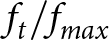 $f_t/f_{max}$ of 470/650 GHz. The back-end-of-line (BEOL) consists of a 12-µm thick seven-metal aluminum stack with two thick top-metal layers, 1.5 fF/µm2 metal-insulator-metal (MIM)-capacitors, and a 256 $\Omega$/sq polysilicon resistor. The cascode stages and the transformers are full-wave 3-D EM co-simulated in Ansys HFSS, including all parasitics and interconnects. All simulations utilize the HiCUM transistor model provided by the foundry for a better correlation between simulation and measurements.
Block diagram of the two-stage LNA with simplified circuit diagram of the  $\times$4 differential cascode topology with biasing networks.
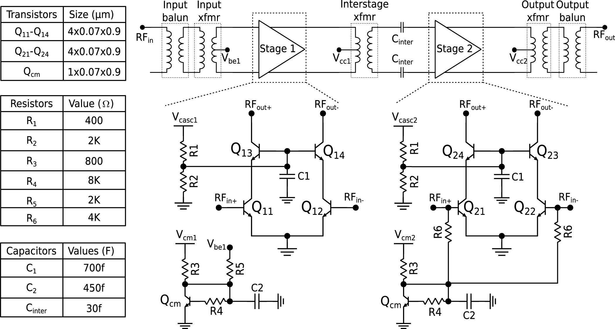
Figure 1 Long description
The diagram shows a two-stage low noise amplifier with detailed circuit components and connections. The transistors are labeled Q subscript 11 to Q subscript 14 and Q subscript 21 to Q subscript 24, each with a size of 4 times 0.07 times 0.9 micrometers and Q subscript cm with a size of 1 times 0.07 times 0.9 micrometers. Resistors are labeled R subscript 1 to R subscript 6 with values of 400 ohms, 2 kilo-ohms, 800 ohms, 8 kilo-ohms, 2 kilo-ohms and 4 kilo-ohms respectively. Capacitors are labeled C subscript 1, C subscript 2 and C subscript inter with values of 700 femtofarads, 450 femtofarads and 30 femtofarads respectively. The input balun and input transformer are connected to the RF subscript in terminal, leading to Stage 1, which is connected to the interstage transformer and capacitor C subscript inter. Stage 2 is connected to the output transformer and output balun, leading to the RF subscript out terminal. The circuit includes connections for V subscript be1, V subscript cc1 and V subscript cc2. The detailed circuit diagram shows transistors Q subscript 11, Q subscript 12, Q subscript 13 and Q subscript 14 connected with resistors R subscript 1 and R subscript 2 and capacitor C subscript 1. Transistors Q subscript 21, Q subscript 22, Q subscript 23 and Q subscript 24 are connected similarly with resistors R subscript 1 and R subscript 2 and capacitor C subscript 1. The circuit also includes connections for V subscript casc1, V subscript casc2, V subscript cm1, V subscript cm2 and Q subscript cm with resistors R subscript 3, R subscript 4, R subscript 5 and R subscript 6 and capacitor C subscript 2.
Due to its lower output capacitance, a 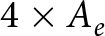 $4 \times A_e$ ( $A_e = 0.07 \times 0.9$ µm2) device size was chosen, enabling low-loss wideband matching. This device size provides the best compromise between minimum noise figure ( $NF_{min}$), maximum available gain ( $G_{max}$), and power consumption. An $NF_{min}$ of 6.6/10 dB and a $G_{max}$ of 17/7 dB at 220/320 GHz, respectively, is achieved at an optimal current density ( $J_{c_{opt}}$) of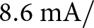 $8.6~\mathrm{mA}/$µm2 ( $I_c$ = 3.3 mA). Due to the limited gain at 320 GHz and to compensate the matching losses, the first stage is biased at a current density of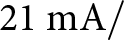 $21~\mathrm{mA}/$µm2 ( $I_c$ = 8 mA), yielding an $NF_{min}$ of 7.2/10.6 dB and a $G_{max}$ of 21.7/10.2 dB at 220/320 GHz, respectively. To improve the overall gain of the amplifier, the second stage is biased at a current density of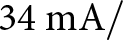 $34~\mathrm{mA}/$µm2 ( $I_c$ = 13 mA).
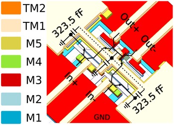
The 3-D model of the cascode core, along with the position of the metal stack, is shown in Figure 2. The input and output are routed from metal 1 (M1) to top metal 1 (TM1) in a vertical staircase configuration similar to [Reference Xingcun, Chen, Zhou, Wang, Huang, Shuyang, Chen and Feng15, Reference Eissa, Malignaggi and Kissinger16], leading to an input differential loss of 0.22 dB and an input differential phase rotation of 12 $^\circ$, and an output differential loss of 0.13 dB and an output differential phase rotation of 10 $^\circ$. MIM capacitors are placed directly above the base of the common-base device, hence reducing the parasitic inductance observed from the inner and outermost fingers of the transistor and improving stability. Ground planes are established all around the cascode device on metal 3 (M3), with an additional vertical ground plane established on metal 1 (M1) along the differential symmetry plane. This allows for better isolation between devices and provides a well-defined current path for the differential and common mode [Reference Andree, Grzyb, Heinemann and Pfeiffer11, Reference Bücher, Grzyb, Hillger, Rücker, Heinemann and Pfeiffer17]. Figure 3 shows the comparison of $G_{max}$ and $NF_{min}$ for a single-stage ideal cascode and the EM-simulated cascode. A gain of 21/12 dB at 220/320 GHz can be achieved with inductive peaking and a noise figure of 7/10 dB at 220/320 GHz. This section investigates the gain and noise figure performance using available gain/power circles (GACs/GPCs) and noise circles (NCs) evaluated at the band edges of 220 GHz and 320 GHz, and subsequently details the transformer design guided by these metrics.
3-D view of the differential cascode core with metal 3 (M3) as ground plane and the input and output routed to top-metal 1 (TM1).

Figure 2 Long description
Insufficient visual information to describe this element accurately.
Comparison plot of maximum available gain ( $G_{max}$) and minimum noise figure ( $NF_{min}$) of the ideal and EM-simulated differential cascode core.

Figure 3 Long description
The plot contains two overlaid line-graph groups against frequency. The x-axis is labeled Frequency (gigahertz), ranging from 150 to 330 with tick marks at 150, 170, 190, 210, 230, 250, 270, 290, 310 and 330. The left y-axis is labeled Gmax (decibel), ranging from 0 to 30 with tick marks at 0, 5, 10, 15, 20, 25 and 30. Two lines are shown for Gmax: one labeled Gmax (Ideal) and one labeled Gmax (EM). Both decrease as frequency increases. At about 150 gigahertz, both are near 25 decibel. Around 190 gigahertz, the ideal curve is near 23 decibel while the EM curve is near 24 decibel. Around 230 gigahertz, the ideal curve is near 20 decibel and the EM curve is near 21 decibel. Around 270 gigahertz, the ideal curve is near 16 decibel and the EM curve is near 17 decibel. Near 330 gigahertz, both are near 12 decibel. The right y-axis is labeled NFmin (decibel), ranging from 6 to 11 with tick marks at 6, 7, 8, 9, 10 and 11. Two lines are shown for NFmin: one labeled NFmin (Ideal) and one labeled NFmin (EM). Both increase as frequency increases. At about 150 gigahertz, both are near 6 decibel. Around 190 gigahertz, the ideal curve is near 6.5 decibel and the EM curve is near 6.7 decibel. Around 230 gigahertz, the ideal curve is near 7.5 decibel and the EM curve is near 7.8 decibel. Around 270 gigahertz, the ideal curve is near 8.6 decibel and the EM curve is near 8.9 decibel. Near 330 gigahertz, the ideal curve is near 10 decibel and the EM curve is near 10.3 decibel. Two oval callouts are drawn: one around the gain curves near about 190 gigahertz and about 22 to 24 decibel and one around the noise-figure curves near about 240 gigahertz and about 7.5 to 8.5 decibel. Two horizontal arrows are drawn: one pointing left near about 15 decibel on the gain scale and one pointing right near about 2 on the gain scale.
Analysis and design
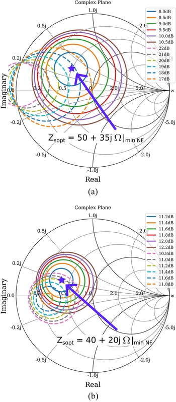
The analysis is carried out using the optimized EM model of the differential cascode core as described in the previous section. To achieve wideband noise matching, two extreme frequencies, 220 and 320 GHz, are considered for the analysis. To facilitate this analysis and to visualize the trade-offs between gain and noise performance, available GACs and NCs are employed. Figure 4 shows the available GACs (dotted) and NCs (solid) plotted on a Smith chart at 220 and 320 GHz. These circles represent the loci of source impedances corresponding to constant available gain and constant noise figure, respectively. The resulting optimal source impedance ( $Z_{sopt}$) of 50+j35 $\Omega$/40+j20 $\Omega$ yields an NF of lower than 8/11.2 dB at 220/320 GHz, respectively.
Analysis of source impedance ( $Z_{sopt}$) using available GACs and NCs for noise optimization. (a) Represents a $Z_{sopt}$ of $50+j35~\Omega$ at 220 GHz, yielding an NF lower than 8 dB, and (b) $Z_{sopt}$ of $40+20j~\Omega$ at 320 GHz, yielding an NF lower than 11.2 dB.

Figure 4 Long description
Two Smith charts illustrate source impedance optimization using available gain circles and noise circles for noise figure minimization. The charts are labeled (a) and (b) for frequencies 220 GHz and 320 GHz, respectively. The x-axis is labeled Real and the y-axis is labeled Imaginary, representing the normalized impedance plane. In chart (a), Zsopt equals 50 plus j35 ohm and in chart (b), Zsopt equals 40 plus j20 ohm, both marked with arrows. The gain circles are dashed, ranging from 8 to 11 decibel and the noise circles are solid, ranging from 17 to 21 decibel. These circles represent loci of constant available gain and noise figure, respectively. The Zsopt points lie near the center of the lowest-noise circle, indicating optimal noise performance. The charts demonstrate the trade-off between gain and noise figure, with shifts in circle positions between the two frequencies.
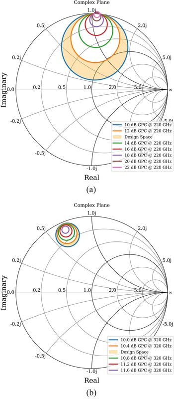
As compared to the input node, the output node presents a significant challenge to achieve wideband matching due to the high Q-factor at the output of the cascode, despite optimizing the layout parasitics. To analyze the sensitivity of the load impedance, GPCs are employed, analogous to the use of GAC and NC. Since the goal of the design is to achieve flat gain, the overall gain of the amplifier is limited by the gain at the higher cut-off frequency of 320 GHz. Figure 5 shows the GPC at 220 and 320 GHz. Unlike the source impedance, a design space with a constant gain of 10 dB is chosen, making the interstage and output transformer design more flexible.
Analysis of load impedance ( $Z_{L}$) using GPCs. (a) Depicts a design space with a constant gain of 10 dB at 220 GHz, and (b) depicts a design space with a constant gain of 10 dB at 320 GHz.

Figure 5 Long description
Panel (a) 220 GHz: A Smith chart showing power gain circles for load impedance analysis. The axes represent the real and imaginary parts of the reflection coefficient. The chart includes contours for gains of 10 to 22 decibels at 220 GHz, with larger circles indicating higher gains. The contours are centered near the upper part of the chart, indicating a wider gain range. Panel (b) 320 GHz: Another Smith chart with similar axes, showing gain circles for 10 to 11.6 decibels at 320 GHz. These contours are more compact and clustered, indicating a narrower gain range. Both panels use the complex plane to visualize impedance matching, with the real axis labeled from 0.2 to 5.0 and the imaginary axis from minus 1.0 to 1.0. The charts help in understanding the design space for achieving constant gain at specified frequencies.
Typical transmission line matching at millimeter-wave frequencies lacks sufficient bandwidth. Although transformers provide larger bandwidths than transmission-line matching above 200 GHz, this design approach fails due to the unavailability of classical transformers operating below the self-resonance frequencies. To overcome this, transformers are implemented as edge-coupled-line sections. However, these coupled line transformers fail to provide large impedance transformation ratios over a large bandwidth. This issue is addressed by implementing the transformer as an asymmetrical broadside coupled line section capable of providing a higher impedance transformation ratio over the required bandwidth. These asymmetrical broadside coupled lines can be expressed in terms of two independent modes, namely “c” and “ $\pi$” modes. The corresponding line impedances are represented as $Z_{ct}$, $Z_{cb}$, and $Z_{\pi t}$, $Z_{\pi b}$ for the top and bottom conductors, respectively. Unlike symmetrical lines, an extra parameter $R_c$ and $R_{\pi}$ is defined as the mode amplitude ratio of the two lines. In case of a symmetric line,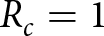 $R_c = 1$ and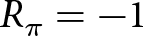 $R_{\pi} = -1$ [Reference Tripathi18–Reference Tsai and Tzuang20]. Taking advantage of the vertical stack of BEOL, all transformers are designed as asymmetrical broadside coupled line sections on TM1 and M4. Additional ground strips are established on M1, which reduces the effective aperture size of the ground opening, hence minimizing the common mode radiation by 40 $\%$ to the substrate and improving common mode stability. Figure 6 shows $ \gt 15~\mathrm{dB}$ improvement in the common-mode suppression at 220 GHz without affecting the differential loss of the transformer.
Simulated differential and common-mode loss of the input transformer with and without the M1 ground strip.

Figure 6 Long description
The y-axis is labeled “Differential/Common-Mode Loss (dB)”. The y-axis ranges from 0 to minus 30, with labeled ticks at 0, minus 2, minus 4, minus 6, minus 8, minus 10, minus 12, minus 14, minus 16, minus 18, minus 20, minus 22, minus 24, minus 26, minus 28 and minus 30. The x-axis is labeled “Frequency (GHz)”. The x-axis ranges from 200 to 330, with labeled ticks at 200, 210, 220, 230, 240, 250, 260, 270, 280, 290, 300, 310, 320 and 330. A legend lists four line series: “Transformer Differential-Loss without M1 Strip”, “Transformer Differential-Loss with M1 Strip”, “Transformer Common-mode Loss without M1 Strip” and “Transformer Common-mode Loss with M1 Strip”. The “Transformer Common-mode Loss with M1 Strip” curve starts near minus 26 at 200 and increases steadily to about minus 8 at 330. The “Transformer Common-mode Loss without M1 Strip” curve starts near minus 6 at 200 and rises gradually to about minus 2 at 330. The two differential-loss curves remain close to 0 across the full frequency range, with small variation around 0 and no large slope visible.
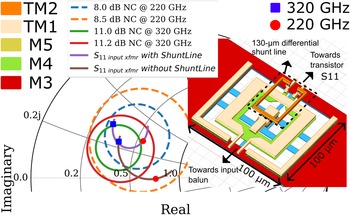
Figure 8 shows the 3-D model of the input transformer and its output impedance trajectory with a 100  $\Omega$ differential input impedance. The input transformer occupies an area of 100 µm $\times$ 100 µm and provides an approximate impedance transformation ratio of 3.3:1 (100–30 $\Omega$) resulting in its output impedance trajectory located inside the ( $\mathrm{NF_{min}}$+1 dB) NCs across the entire J-band which are exemplarily shown for 220 GHz (8.0 dB NC) and 320 GHz (11.0 dB NC) in Figure 8. The highlighted 130 µm differential shunt line implemented on top-metal 2 further increases the inductive behavior of the transformer output impedance, resulting in an impedance of 52+24j $\Omega$ at 220 GHz and a loss of $-$1.1 dB to $-$1.3 dB in the range of 200–320 GHz as shown in Figure 7. The interstage and output transformers are optimized at 320 GHz and ensure a constant gain of 10 dB from 220 to 320 GHz, which is close to its peak gain of 10.8 dB at 320 GHz, excluding transformer losses. The interstage transformer is designed as an asymmetric broadside coupled line on TM1 and M4 in combination with a 30 fF series capacitance to achieve an impedance transformation from 30 $\Omega$ (input of second stage) to 150 $\Omega$ (output of first stage). Unlike the input transformer, the interstage transformer is designed as a tapered asymmetrical broadside coupled line section, providing a distributed loading effect and making the transformer compact and extremely wideband with a larger transformation ratio of 5:1. It occupies an area of 80 µm $\times$ 65 µm as shown in Figure 9(b). Figure 7 shows the loss of the interstage transformer, with a minimum loss of $-$1.8 dB at 320 GHz and $-$6 dB at 220 GHz, hence maintaining a constant gain across the BW. The impedance trajectory of the interstage transformer when loaded with differential input impedance of the following stage ( $R_{ser} \approx$30 $\Omega$ and $C_{ser}\approx$25 fF), together with the GPCs of the first stage at 220 and 320 GHz, are shown in Fig. 9(a). In more detail, the impedance trajectory lies within the 9–10 dB GPC across the entire bandwidth, achieving a flat gain characteristic. Furthermore, it has been simulated for slightly varying device output capacitances, showing a similar gain characteristic, thus accounting for device model uncertainties and ensuring proper operation above 300 GHz. Figure 10 depicts the Smith chart trajectory of the interstage transformer for different taper angles $\alpha$, where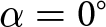 $\alpha=0^\circ$ corresponds to an untapered line. Increasing the taper angle enhances the distributed impedance gradient along the structure, thereby increasing the effective impedance transformation ratio. As the taper angle increases, the trajectory moves into the 10 dB at 320 GHz, leading to a stronger transformation from the input impedance of 52-24j $\Omega$ presented by the input of the second stage. At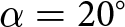 $\alpha=20^\circ$, the targeted 5:1 transformation ratio is achieved while maintaining a broadband match.
Simulated losses of input, interstage, and output transformers with respective impedance loading.

Input impedance transformation (S $_{11}$ input transformer) with and without the differential shunt line overlapping the EM simulated NCs at 220/320 GHz and the 3-D model of the input transformer with the 130-µm differential shunt line.

Figure 8 Long description
Two sub-images are present. The image A showing a Smith chart plotting the input reflection coefficient labeled S11, representing the input impedance trajectory of a transformer. Four trajectory curves are shown, each corresponding to a distinct condition. Two curves represent S11 input at 220 gigahertz and 320 gigahertz with the differential shunt line. Two additional curves represent S11 input at 220 gigahertz and 320 gigahertz without the shunt line. Two circular overlays represent electromagnetically simulated noise circles labeled NC at 220 gigahertz with 8.0 decibel NC and at 320 gigahertz with 11.0 decibel NC. The trajectories with the shunt line sit closer to the center of the Smith chart compared to those without, indicating improved impedance matching. The trajectory labels include five named curves in the legend: TM2 at 8.0 decibel NC at 220 gigahertz, TM1 at 8.5 decibel NC at 220 gigahertz, M5 at 11.0 decibel NC at 320 gigahertz, M4 at 11.2 decibel NC at 320 gigahertz and M3. Two directional labels are present indicating the path toward the input and toward the transistor or load. The image B showing a 3D layout drawing of the input transformer structure. The structure is square with nested rectangular conductor paths forming a transformer geometry. A label identifies a 130 micro meter differential shunt line implemented on the top metal layer. A dimension marking along one edge reads 100 micro meter, indicating the overall footprint of the transformer. Labels on the structure identify the S11 input port direction and the S11 load direction, corresponding to the trajectory endpoints shown in the Smith chart.
(a) Interstage (S $_{11}$ interstage transformer) and output impedance (S $_{22}$ output transformer) transformation overlapping GPCs at 220/320 GHz. (b) 3-D model of the interstage transformer with a 30 fF series capacitor and output transformer with a 50-µm, 35 $\Omega$ differential series line.

Figure 9 Long description
The image A showing a Smith chart displaying normalized impedance trajectories labeled S11 interstage and S11 output, overlaid with constant power gain circles at 220 gigahertz and 320 gigahertz. The Smith chart uses normalized resistance circles and reactance arcs to represent the complex reflection coefficient magnitude and phase. The S11 label refers to the input reflection coefficient, indicating how closely the transformer output impedance matches the desired load. Five impedance trajectory curves are shown, each corresponding to a metal layer stack option labeled TM2, TM1, M5, M4 and M3. The power gain circles are plotted at levels of 9.0 decibel, 10.0 decibel, 10.2 decibel, 10.4 decibel, 10.6 decibel and 10.8 decibel at 320 gigahertz and 9.0 decibel, 10.0 decibel at 220 gigahertz, as indicated in the legend. The S11 interstage trajectory at 320 gigahertz falls within the 10.0 to 10.8 decibel power gain circles, while the trajectory at 220 gigahertz falls within the 9.0 to 10.0 decibel power gain circles. The metal layer traces differ in their proximity to the chart center and their containment within specific gain circles, with TM2 and TM1 positioned closer to the center compared to M5, M4 and M3. The image B showing two 3D structural models side by side. The left model is labeled interstage transformer and shows a layered transmission line structure with a 30 femtofarad series capacitor. Annotations indicate the direction towards the input of stage 2 and the S11 interstage output of stage 1. The structure occupies a footprint labeled 80 micrometers by 65 micrometers, with a taper angle labeled alpha. The right model is labeled output transformer and shows a similar layered structure with annotations indicating the direction towards the output balanced-to-unbalanced converter and towards the transistor. The footprint is labeled 80 micrometers by 55 micrometers, also with a taper angle labeled alpha. Both models display multiple metal layers rendered in distinct shading to indicate layer separation.
Sweep of taper angle of the interstage transformer with the output of the transformer (towards the input of stage 2) being loaded with the input impedance of the second stage.

Figure 10 Long description
The Smith chart displays S11 trajectories for different taper angles, representing the input reflection coefficient on a normalized impedance plane. The chart includes five trajectories for taper angles of 0, 5, 10, 15 and 20 degrees. The gain circles, labeled as GPC, indicate constant gain contours at 220 gigahertz (9 and 10 decibels) and 320 gigahertz (10.0 to 10.8 decibels). The S11 trajectories show how the reflection coefficient varies with taper angle, with the 20-degree taper moving closer to the center, indicating better matching and lower reflection. The dashed trajectory extends toward higher positive reactance, showing increased inductive behavior. The chart helps in selecting taper angles that align S11 within higher-gain regions, optimizing performance at the specified frequencies.
The output transformer is designed following the same principle as the interstage transformer, employing a tapered asymmetrical broadside-coupled line section on TM1 and M4. A similar taper profile of 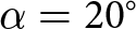 $\alpha=20^\circ$ is adopted to achieve a gradual variation in impedance along the structure, enabling broadband impedance transformation. Figure 9 shows the impedance trajectory and the 3-D model of the output transformer occupying an area of 80 µm $\times$ 65 µm. It is designed in combination with a capacitively coupled 50 µm, 35 $\Omega$ series differential line to achieve an impedance transformation from 100 $\Omega$ to 25+70j $\Omega$ (4:1) while maintaining a 10 dB gain from 220 to 320 GHz. The insertion loss of the output transformer follows a trend similar to that of the interstage transformer, with a minimum of $-$2.1 dB at 320 GHz and $-$5 dB at 220 GHz, as shown in Figure 7.
Measurements
The chip micrograph of the LNA with a core amplifier area of 0.053 mm $^2$ is shown in Figure 11(a). Two additional Marchand baluns, placed at the LNA input and output, compensate for the parasitic pad capacitance, allowing broadband on-wafer measurements. A single balun/pad combination covers the entire J-band, featuring a measured insertion loss of 1.3 - 1.5 dB [Reference Grzyb, Andree, Hillger, Bücher and Pfeiffer21]. The balun layout provides good common-mode suppression similar to Figure 6 due to its asymmetrical layout, which features a ground pattern that prevents common-mode propagation to the substrate. To characterize the LNA as a standalone circuit, the influence of the baluns has been de-embedded from the measured gain and NF.
(a) Chip micrograph of the two-stage LNA with a core size of 382 µm  $\times$ 140 µm. (b) Measurement setup for 1) small-signal with OML-Modules and 2) large-signal measurements using the AMC378 and 379 modules.

Figure 11 Long description
The image consists of two parts. The first part shows a chip micrograph of a two-stage low-noise amplifier. The micrograph is rectangular, measuring 765 micrometers by 440 micrometers, with a core size of 382 micrometers by 140 micrometers. It features an input/output matching transformer labeled at the top center and a balun labeled at the bottom center. The input is marked on the left and the output is marked on the right. The second part illustrates a measurement setup. It includes two configurations: 1) small-signal measurement using OML Modules operating between 220 to 325 gigahertz, connected to the device under test (DUT) via input and output probes. 2) large-signal measurement using AMC 378 and 379 modules with a variable attenuator, also connected to the DUT. The output is connected to a power meter labeled PM 4. The setup is designed for testing the performance of the LNA.
The measurement setup is shown in Figure 11(b). Two out-of-band (200–330 GHz) calibrated J-band frequency extension modules from OML are connected to a Keysight P8361A vector network analyzer for small signal measurements. The measurement is performed on 35 samples after an initial Line-Reflect-Match calibration on a standard CS-15 calibration substrate from GGB Industries. The results of the best sample have been presented in this paper
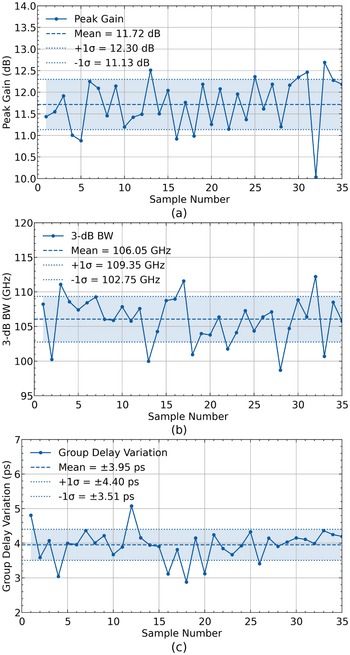
Simulated and measured S-parameters and the simulated NF are shown in Fig. 12. With  $S_{11}$ values smaller than 10 dB and $S_{22}$ values below 7 dB, the input and output are well matched across the whole J-band. $S_{12}$ is typically below $-$40 dB. A maximum $S_{21}$ of 11.8 dB is achieved at 295 GHz, covering a broad 111 GHz 3-dB bandwidth spanning from 211 to 322 GHz. The measured and simulated $S_{21}$ values correlate well, showing a similar trend and a deviation of $ \lt 0.5~\mathrm{dB}$/stage across the entire operating range. In contrast to previous publications [Reference Andree, Grzyb, Heinemann and Pfeiffer11, Reference Bücher, Grzyb, Hillger, Rücker, Heinemann and Pfeiffer22], no faster gain roll-off was present in the measured LNA gain above 300 GHz. This confirms the complex design approach, ensuring a constant LNA gain across varying device output capacitances that may arise from inaccurate device models above 300 GHz. Due to the unavailability of a J-band noise source and the low LNA gain, only NF simulations are presented. The minimum NF is 9.7 dB at 226 GHz, and it increases to 14 dB at 330 GHz. In Figure 13, the measured and simulated group delay and k-factor of the LNA are presented. With a minimum value higher than 14.5 measured at 234 GHz, the k-factor indicates stable LNA operation from 200 to 330 GHz. With a maximum value of 20.5 ps around 320 GHz and a minimum value of 13 ps at 242 GHz, the variation of the measured group delay stays within $\pm 3.8$ ps. Additionally, 35 samples were measured, and Figure 14 shows the variation of peak gain, BW, and GD across the samples. The LNA has an average peak gain/BW/GD variation of 11.71 dB/109 GHz/3.95 ps with 70 $\%$ of the samples within $\pm1\sigma$. The sample with the largest bandwidth is selected, showing a deviation of less than 1% in peak gain and 5% in group delay relative to the mean values.
Measured and simulated small-signal s-parameters with a peak gain of 11.8 dB at 295 GHz and simulated LNA NF and the single-stage  $NF_{min}$.

Figure 12 Long description
The graph shows measured and simulated small-signal S-parameters and noise figure versus frequency. The x-axis is labeled frequency in GHz, ranging from 200 to 330. The left y-axis is labeled S-parameter in decibel, ranging from -50 to 10. The right y-axis is labeled noise figure in decibel, ranging from 0 to 14. The plot includes several curves: S11 (measured and simulated), S21 (measured and simulated), S12 (simulated), S22 (simulated) and noise figure (simulated). The S11 curves show input return loss, with dips around 240 GHz and 300 GHz. The S21 curves indicate forward gain, peaking at 295 GHz with a maximum gain of 11.8 decibel. The S12 curve represents reverse isolation, remaining below -40 decibel. The S22 curve shows output return loss. The noise figure curve rises from 9.7 decibel at 226 GHz to 14 decibel at 330 GHz. The plot highlights the performance of the low-noise amplifier across the J-band frequency range.
Measured and simulated group delay and k-factor of the LNA including the baluns. The group delay stays within  $\pm 3.8$ ps and k-factor $ \gt 5$.

Figure 13 Long description
Simulated GD Measured GD Simulated k-factor Measured k-factor A dual-axis line graph with frequency on the horizontal axis. The horizontal axis is labeled Frequency (GHz), with tick labels from 200 to 330 in steps of 10. The left vertical axis is labeled Group Delay (ps), with tick labels from 12.5 to 30.0 in steps of 2.5. The right vertical axis is labeled K-factor, with tick labels from 0 to 80 in steps of 10. Four line series are shown: Simulated GD, Measured GD, Simulated k-factor and Measured k-factor. Group delay traces: The group delay values lie mainly between about 13 and about 22 ps across the frequency range. The measured group delay line shows multiple small peaks and dips between 200 and 260 GHz, then continues with smaller variations from about 260 to 330 GHz. The simulated group delay line is smoother and trends downward from the low 20 ps range near 200 GHz toward the mid to high teens by about 330 GHz. K-factor traces: The k-factor lines are near the lower part of the right-axis scale for most frequencies. A narrow, tall peak is present in the k-factor around the mid-200 GHz region, rising to near the top of the 0 to 80 scale, then returning to lower values after the peak. The simulated and measured k-factor traces follow similar overall placement, with the sharp peak visible on the k-factor series.
Measured sample variation across 35 samples showing (a) peak gain with an average of 11.72 dB, (b) 3-dB BW with an average of 106 GHz, and (c) group delay variation of 3.95 ps.

Figure 14 Long description
Three vertically stacked line graphs labeled a, b and c. a) Legend text: Peak Gain; Mean equals 11.72 decibel; plus 1 sigma equals 12.30 decibel; minus 1 sigma equals 11.13 decibel. Horizontal axis label: Sample Number. Horizontal axis range: 0 to 35. Vertical axis label: Peak Gain (decibel). Vertical axis range: 10.5 to 14.0. The plotted line shows multiple peaks and dips across the sample numbers, with a low point near sample number 33 close to 10.5 and higher points near sample numbers 31 to 35 around 12.5 to 13.0. b) Legend text: 3 dash decibel BW; Mean equals 106.05 GHz; plus 1 sigma equals 109.35 GHz; minus 1 sigma equals 102.75 GHz. Horizontal axis label: Sample Number. Horizontal axis range: 0 to 35. Vertical axis label: 3 dash decibel BW (GHz). Vertical axis range: 95 to 120. The plotted line varies across the samples, with values near 100 to 110 for many samples, a higher point near sample number 15 around 112 and higher points near sample numbers 33 to 35 around 115 to 118. c) Legend text: Group Delay Variation (ps); Mean equals 3.95 ps; plus 1 sigma equals 4.40 ps; minus 1 sigma equals 3.51 ps. Horizontal axis label: Sample Number. Horizontal axis range: 0 to 35. Vertical axis label: Group Delay Variation (ps). Vertical axis range: 2 to 7. The plotted line fluctuates around 4, with a higher point near sample number 10 around 5.5, a lower point near sample number 18 around 3.0 and values near 4.0 to 4.5 from about sample number 25 to 35.
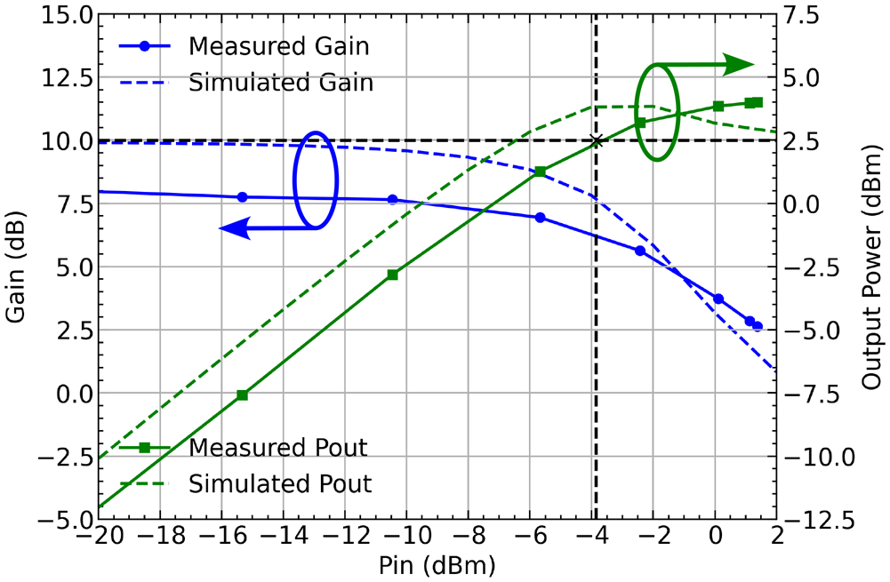
As shown in Figure 11(b), VDI’s amplifier multiplier chain (AMC) 378 (219–270 GHz) and AMC379 (270–330 GHz) modules were used to drive the LNA input for large-signal measurements. The AMC378 ( $\times 24$) comprises a preamplifier, a quadrupling amplifier, a doubler followed by a tripler, while the AMC379 ( $\times 24$) includes a preamplifier, a doubling amplifier, two cascaded doublers followed by a tripler, generating an output power of 6.5–9.5 dBm. The input power to the LNA is controlled using a mechanical attenuator with an attenuation range of $-$1.5 to $-$30 dB in the J-band and an accuracy of $\pm$0.5 dB, and the output is connected to a PM4 power meter. Due to the losses of the waveguide bend and probe at the input (7.5 dB at 310 GHz), a maximum power of 2 dBm is available at the input of the LNA. The waveguide bend and probe losses at the output (7.75 dB at 310 GHz) are de-embedded from the measured output power. Figure 15 shows the compression curves of the LNA, including the balun losses at 310 GHz, with a measured saturated output power ( $P_{sat}$) of 4.0 dBm and an $OP_{1dB}$ of 2.5 dBm. Figure 16 shows the $P_{sat}$ and the $OP_{1dB}$ curve across the J-band, including the losses of the balun. A third-order polynomial fit was done on the measured data, showing good correlation with the simulated curves. The LNA has a peak $P_{sat}$ of 4.65 dBm at 280 GHz with a corresponding $OP_{1dB}$ and $IP_{1dB}$ of 3.6 and $-$4.6 dBm, respectively.
Measured and simulated output power and power gain at 310 GHz, including the balun losses.

Figure 15 Long description
A plot with two line graphs on the same axes area. Legend text: Measured Gain. Simulated Gain. Measured Pout. Simulated Pout. Horizontal axis label: Pin (decibel milliwatt). Horizontal axis range: negative 20 to 0. Left vertical axis label: Gain (decibel). Left vertical axis range: negative 5.0 to 15.0. Right vertical axis label: Output Power (decibel milliwatt). Right vertical axis range: negative 12.5 to 7.5. Plotted series: 1. Measured Gain: A curve that rises from near 0 gain at Pin around negative 20, reaches a higher region around 10 to 12 gain near Pin around negative 10 to negative 6, then decreases toward lower gain as Pin approaches 0. 2. Simulated Gain: A curve that follows a similar rise and then a decrease, staying close to the measured gain curve across the Pin range. 3. Measured Pout: A curve that increases as Pin increases, starting near the lower part of the right axis at Pin around negative 20 and reaching near the upper part of the right axis as Pin approaches 0. 4. Simulated Pout: A curve that increases with Pin and stays close to the measured output power curve across the Pin range. Two vertical dashed reference lines are drawn at Pin equals negative 6 and Pin equals negative 4.
Measured and simulated  $P_{sat}$ and $OP_{1dB}$ with a peak $P_{sat}$ of 4.65 dBm and an $OP_{1dB}$ of 3.6 dBm at 280 GHz, including the balun loss.

Figure 16 Long description
The graph displays output power in decibels on the vertical axis, ranging from negative 5 to 6 and frequency in gigahertz on the horizontal axis, ranging from 200 to 330. It includes six lines: simulated Psat (solid blue), measured Psat (blue circles), measured Psat fit (dashed blue), simulated OP1dB (solid red), measured OP1dB (red squares) and measured OP1dB fit (dashed red). The simulated Psat line peaks around 4.5 dBm near 280 GHz, while the measured Psat line peaks slightly lower. The simulated OP1dB line peaks around 3.5 dBm, also near 280 GHz, with the measured OP1dB line following a similar trend but at a lower level. The graph shows how the measured data closely follows the simulated data, with both sets peaking around the same frequency range.
Conclusion
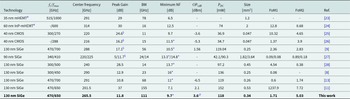
This paper presents the analysis of a two-stage pseudo-differential cascode LNA implemented in IHP’s 130-nm SiGe HBT technology (SG13G3), demonstrating 70%/100% of the samples within 1 $\sigma$/3 $\sigma$. Based on a broadband, fully EM co-simulated transformer-based matching network, the LNA covers the IEEE 802.15.3d-2017 band and nearly the entire J-band. The proposed design achieves a 3-dB bandwidth of 111 GHz (211–322 GHz) with a peak gain of 11.8 dB, representing the widest bandwidth reported for silicon-integrated, reactively matched LNAs operating above 300 GHz, as summarized in Table 1. A modified figure of merit (FoM) is introduced to account for high-frequency design complexity and enable a fair comparison with prior work. Using this metric, the proposed LNA demonstrates state-of-the-art performance and outperforms 90 $\%$ of reported designs above 200 GHz. The LNA exhibits a $P_{sat}~ \gt 2~\mathrm{dBm}$ and an $OP_{1dB}~ \gt 0~\mathrm{dBm}$ from 220 to 330 GHz. Furthermore, the measured group delay variation of $\pm$3.8 ps corresponds to less than 10% of the symbol duration for a 100 Gb/s 16-QAM signal, highlighting its suitability for low-latency, broadband wireless communication systems.
State-of-the-art silicon LNAs operating above 200 GHz

Table 1 Long description
The table compares published low-noise amplifiers operating above 200 GHz across technologies, listing transistor speed, center frequency, peak gain, bandwidth, minimum noise figure, output compression point, DC power, chip area, and two figures of merit. Center frequencies span about 201.5 to 314 GHz, with gains from 5 to 37 dB and bandwidths from 11 to 155 GHz. The strongest overall entry is a 130 nm SiGe design at 201.5 GHz with 37 dB gain, 155 GHz bandwidth, 7.1 dB minimum noise figure, 2.1 dBm output compression, 152 mW power, and the highest FoM1 at 1237.9. The widest bandwidth among the remaining entries is 111 GHz for a 130 nm SiGe design at 265.5 GHz, while a 35 nm mHEMT waveguide LNA reports 29 dB gain over 78 GHz bandwidth at 291 GHz but does not report power or figures of merit. CMOS entries around 216 to 220 GHz show moderate gain, about 16.2 to 24.6 dB, narrower bandwidth, 11 to 15 GHz, and minimum noise figures around 9.7 to 11.5 dB, with power near 35 mW and very small area at 0.047 square millimeters. The “This work” 130 nm SiGe result at 265.5 GHz reports 11.8 dB gain, 111 GHz bandwidth, 9.7 dB minimum noise figure, 118 mW power, 0.34 square millimeters area, FoM1 of 1.71, and FoM2 of 5.03. Some noise figures are marked as simulated rather than measured, and one output compression value includes balun loss, so direct comparisons should be made with caution.
* Simulated, $ Gain boosted, # Waveguide LNA, β With balun loss, FoM1 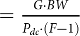 $= \frac{G\cdot BW}{P_{dc}\cdot(F-1)}$, FoM2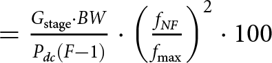 $ = \frac{G_{\mathrm{stage}}\cdot BW}{P_{dc}(F-1)} \cdot \left(\frac{f_{NF}}{f_{\max}}\right)^2 \cdot 100$
Funding statement
The research work presented in this paper was funded by the German Research Foundation (“Deutsche Forschungsgemeinschaft”) (DFG) under project ID 287022738 TRR 196 for project C08.
Competing interests
The author(s) declare none.

Arjith Chandra Prabhu received the B.Sc. degree in Electronics and Communication from PES Institute of Technology, Bengaluru, India, in 2018 and the M.Sc. degree in Electrical Engineering and Information Technology from Karlsruhe Institute of Technology (KIT), Germany, in 2021. He is currently pursuing his Ph.D degree at the Institute of High Frequency and Communication Technology, University of Wuppertal, Germany. He has received the European Microwave Components (EuMC) Young Engineers Prize (YEP) at the 2025 EuMW conference. His main research focus is on mm-Wave and THz signal generation for high-resolution imaging and communication.

Dr Janusz Grzyb received the M.Sc. degree (cum laude) in electronic engineering from the Integrated Circuits Laboratory, Gdansk University of Technology, Gdansk, Poland, in 1998, and the Ph.D. degree from the Swiss Federal Institute of Technology, Zurich, Switzerland, in 2004. From 2004 to 2006, he was with the Communication System Design and High-Speed/Optical Packaging Groups, IBM T. J. Watson Research Center, Yorktown Heights, NY, USA. From 2006 to 2009, he was with the Research and Development Group, Huber&Suhner, Pfaffikon ZH, Switzerland. From 2009 to 2024 he was with the Institute for High-Frequency and Communication Technology, University of Wuppertal, Wuppertal, Germany. His research interests include all aspects of silicon-integrated THz electronics.

Dr Marcel Andree received the M.Sc. degree and Ph.D. degree (passed with honors) in electrical engineering from the University of Wuppertal, Wuppertal, Germany, in 2017 and 2023, respectively, where he focused on the development and optimization of integrated mixed-signal circuits and silicon-integrated circuits for THz imaging applications. Since 2017, he has been a Research Staff Member with the Institute for High-Frequency and Communication Technology (IHCT), Wuppertal. Currently, he is a Postdoctoral Researcher and Group Leader for integrated circuit design at the University of Wuppertal. His research interests include terahertz integrated circuit and system design in silicon technologies. He is a co-recipient of the 2025 European Microwave Integrated Circuits Conference (EuMIC) Best Paper Prize.

Zhichu Cao received the B.Sc. degree in the School of Electronic Information and Electrical Engineering from Shanghai Jiao Tong University, Shanghai, China, in 2018, and M.Sc. in electrical engineering from the University of Wuppertal, Wuppertal, Germany, in 2024. She is currently pursuing a Ph.D. degree with the Institute for High Frequency and Communication Technology, University of Wuppertal, Wuppertal, Germany. Her main research interest is terahertz integrated circuits and system design in silicon technologies.

Dr Holger Rücker received the Diploma and Doctorate degree in physics from the Humboldt University of Berlin, Berlin, Germany, in 1986 and 1988, respectively. From 1989 to 1991, he was a Staff Member with the Humboldt University of Berlin. From 1991 to 1992, he was with the Max Planck Institute for Solid State Research, Stuttgart, Germany. In 1992, he joined IHP, Frankfurt (Oder), Germany, where he is engaged in research on the physics and fabrication of semiconductor devices. He has also led the development of IHP’s 130-nm SiGe BiCMOS technologies SG13S, SG13G2, and SG13G3. His research interests include SiGe bipolar devices, the development of CMOS and BiCMOS technologies, and their application in radio-frequency integrated circuits.

Dr Ullrich R. Pfeiffer received the diploma degree and Ph.D. degree in physics from the University of Heidelberg, Heidelberg, Germany, in 1996 and 1999, respectively. In 1997, he worked as a Research Fellow with the Rutherford Appleton Laboratory, Oxfordshire, England. From 1999 to 2001, he worked as a Postdoctoral Researcher with the University of Heidelberg and with the European Organization for Nuclear Research (CERN), Geneva, Switzerland. From 2001 to 2006, he was with the IBM T.J. Watson Research Center, Yorktown Heights, NY, USA. Since 2008, he has been holding the High-Frequency and Communication Technology chair at the University of Wuppertal, Wuppertal, Germany. His current research interests include silicon RFICs for mmWave/THz communications, radar, and imaging systems.














 Open access

