


1 Introduction
Spatial light modulators (SLMs) enable arbitrary shaping of near-field beam profiles[ Reference Li, Wang, Lu, Ding, Du, Chen, Zheng, Ba, Dong, Yuan, Bai, Liu and Cui 1 – Reference Lin, Zhong, Wu, He, Chen, Hu, Chen and Yu 3 ]. Their dynamic reshaping flexibility and programmability are indispensable for beam shaping, wavefront controlling and additive manufacturing[ Reference Sun, Dai, Lin, Qiao, Zhang, Li and Ruan 4 – Reference Kumar, Gupta, Ghosh and Banerjee 7 ]. Optically addressed spatial light modulators (OASLMs) offer higher optical transmittance and avoid the black matrix effect compared with conventional electrically addressed SLMs[ Reference Huang, Fan, Cheng, Xia, Pei, Li and Lin 8 ]. These devices have been used in the high-power-laser facility for spatial beam shaping at the Lawrence Livermore National Laboratory (LLNL, United States), called the National Ignition Facility, since 2010[ Reference Heebner, Borden, Miller, Hunter and Dinicola 9 , Reference Heebner, Borden, Miller, Stolz, Suratwala, Wegner, Hermann, Henesian, Haynam, Hunter, Christensen, Wong, Seppala, Brunton, Tse, Awwal, Franks, Marley, Williams, Scanlan, Budge, Monticelli, Walmer, Dixit, Widmayer, Wolfe, Bude, McCarty and DiNicola 10 ]. Currently, OASLMs are deployed in major high-power-laser facilities such as the Shenguang facility series in China[ Reference Fan, Jiang, Wang, Wang, Huang, Lu, Wei, Li, Pan, Qiao, Wang, Cheng, Zhang, Huang, Xiao, Zhang, Li, Zhu and Lin 11 , Reference Jiang, Wang, Ding, Liu, Yang, Li, Huang, Cao, Yang, Hu, Miao, Zhang, Wang, Yang, Yi, Tang, Kuang, Li, Yang and Zhang 12 ], OMEGA-EP system in the United States[ Reference Barczys, Bahk, Spilatro, Coppenbarger, Hill, Hinterman, Kidder, Puth, Touris and Zuegel 13 ] and Laser Mégajoule device in France[ Reference Julien, Adolf, Bar, Beau, Bordenave, Chiès, Courchinoux, Di-Nicola, Féral, Gendeau, Graillot, Grosset-Grange, Henry, Higonenq, Journot, Lacampagne, Lafond, Le Déroff, Martinez, Patissou, Roques, Thauvin and Thiell 14 ].
The application of OASLMs in high-power lasers saves considerable operational costs by improving the beam shaping accuracy and avoiding frequent optics replacement[ Reference Huang, Fan, Cheng, Wei, Wang, An, Wang, Cheng, Xia, Li and Lin 15 ]. To meet the demand for higher-precision dynamic beam shaping, next-generation OASLMs[ Reference Chatterjee, Ghandiparsi, Gottlieb, Shao, Frye, Harrison and Voss 16 – Reference Gu, Niu, Liu, He, Yao, Yi, Wang, Xun and Liu 18 ] must withstand laser intensities exceeding the current limit. In high-power, high-repetition-rate laser systems, the dominant failure mechanism is not optical breakdown[ Reference Sharma and Rieckhoff 19 ], but rather performance degradation induced by thermal accumulation[ Reference Zhang, You and Chu 20 ]. The absorption coefficient of indium tin oxide (ITO) is high[ Reference Han, Fan, Song, Huang, Cheng, Pan and Lin 21 ]; therefore, under high-average-power laser irradiation, the resulting heat accumulation rapidly increases the temperature of ITO. In an OASLM, this drives the adjacent nematic liquid crystal (LC) layer beyond its clearing point and imposes excessive thermal stress on the electro-optic Bi12SiO20 (BSO) crystal, which ultimately fractures[ Reference Ghandiparsi, Chatterjee, Shen, Gottlieb, Frye, Schneider, Muir, Buckley, Harrison, Shao, Varley and Voss 22 ].
Han et al. [ Reference Han, Fan, Cheng, Huang and Chen 23 ] showed that decreasing the incident laser spot size increased the tolerated power density of an OASLM but decreased the total tolerated power. Song et al. [ Reference Song, Fan, Sun, Huang, Cheng, Pan and Wang 24 ] replaced a conventional K9 glass substrate with sapphire and fabricated a gallium nitride-based OASLM that delivered an on/off contrast of 256:1 while achieving a peak power density of 2534 W/cm2 using a small spot. Chen et al. [ Reference Chen, Shen, Duan, Qiao, Zeng, Li, Li, Luo, Wang, Shen, Zhao and Zhang 25 ] fabricated an OASLM that remained operational when irradiated by a 352 W, 2.2 mm spot for 10 s. Hamamatsu[ 26 ] reported a liquid crystal on silicon (LCOS) that incorporated high-thermal-conductivity materials and a water-cooling module, thereby enabling continuous laser irradiation at 700 W.
Traditionally, in an OASLM, two ITO layers are deposited onto the surfaces of K9 glass and a BSO crystal, whose thermal conductivities – 1.4 W/(m·K)[ Reference Han, Fan, Cheng, Huang and Chen 23 ] and 3 W/(m·K)[ Reference Ghandiparsi, Chatterjee, Shen, Gottlieb, Frye, Schneider, Muir, Buckley, Harrison, Shao, Varley and Voss 22 ], respectively – are extremely low to dissipate the absorbed heat efficiently. Sapphire, with κ ≈ 45 W/(m·K), offers an order-of-magnitude improvement. Du et al. [ Reference Du, Huang, Cheng, Fan, Xing, Zhu and Liu 27 ] developed a sapphire bonding scheme that exhibited a higher continuous-wave (CW) laser resistance of 100 W/cm2 compared to a K9 substrate OASLM; however, this scheme suffers from bonding strength degradation. In this study, we designed a novel three-layer voltage division architecture that overcomes this limitation.
2 Design parameters of a liquid crystal cell based on bilateral-sapphire substrates with an air gap
In our OASLM design, the ITO electrode is shifted from the BSO surface to a separate sapphire window, and the two crystals are bonded using an ultraviolet (UV) light-curable adhesive. The adhesive layer causes a micrometer-scale air gap (κair ≈ 0.025 W/(m·K)) between the sapphire and BSO layers. This gap acts as a thermal buffer that prevents the temperature rise of the ITO layer from being efficiently conducted into the BSO crystal, thereby mitigating cracking caused by excessive thermal stress. The LC, BSO crystal and air layers between the two ITO electrodes share a voltage. The photoconductive properties of BSO are used to control the voltage across the LC layer. OASLMs achieve beam intensity shaping by coupling the polarization-rotation characteristics of twisted nematic LCs with a pair of polarized beam-splitting prisms[ Reference Wang, Cao, Guo, Xu, Chen and Hu 28 ].
The OASLM architecture based on bilateral-sapphire substrates with an air gap is shown in Figure 1. The device can modulate near-infrared light by addressing a 460 nm blue light.
Schematic of the OASLM based on bilateral-sapphire substrates with an air gap.

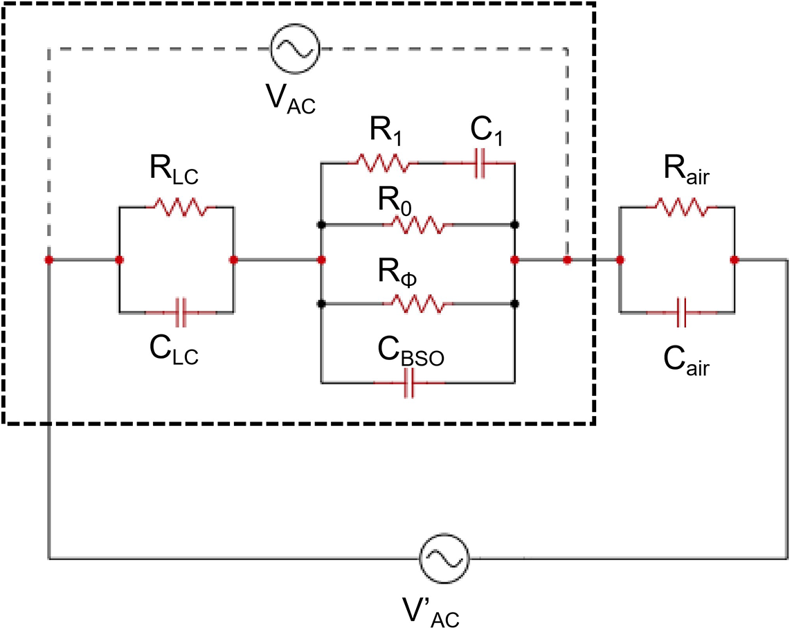
The equivalent circuit of the new OASLM structure is based on the circuit of a traditional OASLM connected in series with an air layer. The air layer is equivalent to a parallel connection between a capacitor and a resistor. The equivalent circuit is shown in Figure 2, where the equivalent circuit of the traditional OASLM is shown in a dashed box[ Reference Aubourg, Huignard, Hareng and Mullen 29 ].
Equivalent circuit model of the OASLM based on bilateral-sapphire substrates with an air gap.

In the equivalent circuit of the traditional OASLM, the voltage division of the LC layer can be expressed as follows:
 $$\begin{align}{V}_{\mathrm{LC}}={V}_{\mathrm{AC}}\frac{\frac{1}{R_0}+\frac{1}{R_{\phi }}+ j\omega {C}_{\mathrm{BSO}}+\frac{j\omega {C}_1}{1+ j\omega {R}_1{C}_1}}{\frac{1}{R_0}+\frac{1}{R_{\phi }}+ j\omega {C}_{\mathrm{BSO}}+\frac{j\omega {C}_1}{1+ j\omega {R}_1{C}_1}+\frac{1}{R_{\mathrm{LC}}}+ j\omega {C}_{\mathrm{LC}}},\end{align}$$
where ${V}_{\mathrm{AC}}$
is the driving voltage of the LC cell,
${V}_{\mathrm{AC}}$
is the driving voltage of the LC cell, ${V}_{\mathrm{LC}}$
is the voltage division of the LC layer,
${V}_{\mathrm{LC}}$
is the voltage division of the LC layer, ${R}_0$
represents the dark resistance of the BSO crystal,
${R}_0$
represents the dark resistance of the BSO crystal, ${R}_{\phi }$
represents the bright resistance of the BSO under blue light irradiation,
${R}_{\phi }$
represents the bright resistance of the BSO under blue light irradiation, ${R}_1{C}_1$
represents the equivalent resistance and capacitance formed by the charge binding effect caused by the photoconductive effect of the BSO crystal,
${R}_1{C}_1$
represents the equivalent resistance and capacitance formed by the charge binding effect caused by the photoconductive effect of the BSO crystal, ${C}_{\mathrm{BSO}}$
represents the capacitance of the BSO layer and
${C}_{\mathrm{BSO}}$
represents the capacitance of the BSO layer and ${R}_{\mathrm{LC}}$
and
${R}_{\mathrm{LC}}$
and ${C}_{\mathrm{LC}}$
respectively represent the resistance and capacitance of the LC layer.
${C}_{\mathrm{LC}}$
respectively represent the resistance and capacitance of the LC layer.
The voltage division formula for the LC layer in the new OASLM structure is as follows:
 $$\begin{align}{V}_{\mathrm{LC}}=V{\hbox{'}}_{\mathrm{AC}}\frac{\frac{1}{\frac{1}{R_{\mathrm{LC}}}+ j\omega {C}_{\mathrm{LC}}}}{\frac{1}{\frac{1}{R_{\mathrm{LC}}}+ j\omega {C}_{\mathrm{LC}}}+\frac{1}{\frac{1}{R_0}+\frac{1}{R_{\phi }}+ j\omega {C}_{\mathrm{BSO}}+\frac{j\omega {C}_1}{1+ j\omega {R}_1{C}_1}}+\frac{1}{\frac{1}{R_{\mathrm{air}}}+ j\omega {C}_{\mathrm{air}}}}.\end{align}$$
To maintain the partial voltage of the LC layer constant at the threshold voltage ${V}_{\mathrm{LC}}$
in the off state, Equations (1) and (2) can be combined to obtain the relationship between
${V}_{\mathrm{LC}}$
in the off state, Equations (1) and (2) can be combined to obtain the relationship between $V{\hbox{'}}_{\mathrm{AC}}$
and
$V{\hbox{'}}_{\mathrm{AC}}$
and ${V}_{\mathrm{AC}}$
as follows:
${V}_{\mathrm{AC}}$
as follows:
 $$\begin{align}V{\hbox{'}}_{\mathrm{AC}}={V}_{\mathrm{AC}}+{V}_{\mathrm{LC}}\frac{\frac{1}{R_{\mathrm{LC}}}+ j\omega {C}_{\mathrm{LC}}}{\frac{1}{R_{\mathrm{air}}}+ j\omega {C}_{\mathrm{air}}}.\end{align}$$
In the equation, ${V}_{\mathrm{AC}}$
= 27 V,
${V}_{\mathrm{AC}}$
= 27 V, ${V}_{\mathrm{LC}}$
= 2.95 V,
${V}_{\mathrm{LC}}$
= 2.95 V, ${R}_{\mathrm{LC}}={\rho}_{\mathrm{LC}}/S$
,
${R}_{\mathrm{LC}}={\rho}_{\mathrm{LC}}/S$
, ${R}_{\mathrm{air}}={\rho}_{\mathrm{air}}/S$
,
${R}_{\mathrm{air}}={\rho}_{\mathrm{air}}/S$
, ${C}_{\mathrm{LC}}={\varepsilon}_{\mathrm{LC}}{\varepsilon}_0S/d$
and
${C}_{\mathrm{LC}}={\varepsilon}_{\mathrm{LC}}{\varepsilon}_0S/d$
and ${C}_{\mathrm{air}}={\varepsilon}_{\mathrm{air}}{\varepsilon}_0S/d$
. The driving voltage of the LC cell was calculated to be 56 V. According to the calculation results, 4.8 μm is a suitable thickness for the air gap based on the existing laboratory conditions and experimental requirements.
${C}_{\mathrm{air}}={\varepsilon}_{\mathrm{air}}{\varepsilon}_0S/d$
. The driving voltage of the LC cell was calculated to be 56 V. According to the calculation results, 4.8 μm is a suitable thickness for the air gap based on the existing laboratory conditions and experimental requirements.
3 Simulation analysis
3.1 Damage mechanism in the new OASLM structure
Pulsed laser damage produces irreversible cracking at the BSO surface of an OASLM, whereas high-average-power laser irradiation damage degrades the LC by a thermally driven reversible (and ultimately permanent) loss of the modulation performance. The dominant pathway is the high absorption coefficient of the transparent ITO electrode (α ≈ 5 × 10⁵ m−1 at 1053 nm). The resulting local heating increases the overall temperature until the LC approaches its clearing point. Under the same driving parameters, the relationship between the transmittance of the LC cell and temperature is as follows[ Reference Li, Gauza and Wu 30 ]:
 $$\begin{align}{T}_{\mathrm{LC}}&=\frac{I}{I_0}=\left(1-R\right)\frac{\sin^2\left(\frac{\pi }{2}\sqrt{N}\right)}{N},\nonumber\\N&=1+{\left(\!\frac{2d\Delta {n}_0}{\pi m\lambda}\left(\!{U}_{\mathrm{LC}}{\left(\!1-\frac{T}{T_\mathrm{C}}\!\right)}^{\frac{\beta }{2}}-\pi m{\left(\!1-\frac{T}{T_\mathrm{C}}\!\right)}^{\beta}\!\right)\!\right)}^2,\end{align}$$
where ${T}_{\mathrm{LC}}$
represents the transmittance of the LC cell,
${T}_{\mathrm{LC}}$
represents the transmittance of the LC cell, $d$
is the thickness of the LC layer,
$d$
is the thickness of the LC layer, $m$
is a parameter related to the elastic coefficient,
$m$
is a parameter related to the elastic coefficient, $\Delta {n}_0$
represents the birefringence of the LC when no voltage is applied,
$\Delta {n}_0$
represents the birefringence of the LC when no voltage is applied, $T$
represents the real-time temperature of the LC layer,
$T$
represents the real-time temperature of the LC layer, ${T}_\mathrm{C}$
represents the clearing point temperature of the LC at 355 K and
${T}_\mathrm{C}$
represents the clearing point temperature of the LC at 355 K and $\beta$
is the material constant of the LC. In this study, the HFS962000-100 LC material produced by Jiangsu Hecheng Display Technology Co., Ltd was used. Its material constant is approximately 0.14–0.2.
$\beta$
is the material constant of the LC. In this study, the HFS962000-100 LC material produced by Jiangsu Hecheng Display Technology Co., Ltd was used. Its material constant is approximately 0.14–0.2.
3.2 Simulation analysis
High-average-power laser heating simulations were conducted based on the Beer–Lambert law and Fourier’s heat conduction equation. The absorption within each layer obeys the Beer–Lambert law as follows:
 $$\begin{align}\frac{\partial I}{\partial Z}=\alpha I\left(1-R\right),\end{align}$$
where $I$
is the laser intensity,
$I$
is the laser intensity, $R$
is the surface reflectivity at 1053 nm and
$R$
is the surface reflectivity at 1053 nm and $\alpha$
is the absorption coefficient at the laser wavelength.
$\alpha$
is the absorption coefficient at the laser wavelength.
When an LC cell is continuously irradiated with a laser, each material layer has a certain laser absorption coefficient, and the device acts as a heat source. The temperature distribution within the device after absorbing a radiation beam is obtained using a partial differential equation of the temperature distribution inside the device according to Fourier’s heat conduction equation, as expressed in Equation (6):
 $$\begin{align}\rho C\frac{\partial T}{\partial t}-\frac{k}{r}\frac{\partial }{\partial r}\left(\frac{\partial T}{\partial r}\right)-k\frac{\partial^2T}{\partial {z}^2}=Q=\alpha I\left(1-R\right),\end{align}$$
where $\rho$
,
$\rho$
, $C$
and
$C$
and $k$
represent the density, constant-pressure heat capacity and thermal conductivity of the material, respectively,
$k$
represent the density, constant-pressure heat capacity and thermal conductivity of the material, respectively, $t$
,
$t$
, $r$
and
$r$
and $z$
represent the time, radial and axial directions of the temperature distribution, respectively, and
$z$
represent the time, radial and axial directions of the temperature distribution, respectively, and $Q$
represents the heat source formed after the device absorbs radiation.
$Q$
represents the heat source formed after the device absorbs radiation.
The temperature rise generated in the device under laser irradiation leads to crystal deformation, resulting in a certain amount of stress that is thermal stress. The distribution of thermal stress within the crystal can be expressed as thermoelastic equations (Equation (7)):
 $$\begin{align}&\rho \frac{\partial^2u}{\partial {t}^2}-\nabla \cdotp \sigma =0,\nonumber\\&\sigma =C:\left(\varepsilon -\beta \left(T-{T}_{\mathrm{b}}\right)\right),\nonumber\\&\varepsilon =\frac{1}{2}{\left({\left(\nabla u\right)}^{\mathrm{T}}+\nabla u\right)}^2, \end{align}$$
where $u$
,
$u$
, $\sigma$
and
$\sigma$
and $\varepsilon$
represent the displacement, thermal stress and thermal strain, respectively,
$\varepsilon$
represent the displacement, thermal stress and thermal strain, respectively, $C$
and
$C$
and $\beta$
represent the elastic tensor and thermal expansion coefficient, respectively, and
$\beta$
represent the elastic tensor and thermal expansion coefficient, respectively, and $T$
and
$T$
and ${T}_{\mathrm{b}}$
represent the real-time temperature of the object and the environment temperature.
${T}_{\mathrm{b}}$
represent the real-time temperature of the object and the environment temperature.
An anti-reflection coating is deposited on each layer of the substrate of the LC cell. Its absorption coefficient at 1053 nm is significantly low to allow it to be neglected to reduce the model complexity and computing time. The model represents a standard 20 mm × 20 mm LC cell comprising 3 mm sapphire windows, 1 mm BSO crystal, 4.8 μm nematic LC and air-gap layers and 50 nm ITO and 100 nm polyimide (PI) alignment layers. A one-quarter geometry with symmetrical planes is used to accelerate the convergence.
As the absorption coefficient of the ITO transparent conductive film under a 1053 nm laser reaches 5 × 10⁵ m−1, the absorption coefficient of the PI film also reaches 104 m−1. The temperature increase of the device is primarily due to heat absorption of the film and energy being conducted into the bulk substrates and ultimately into the LC layer, thereby driving the LC toward its clearing point and causing a loss of modulation capacity. The material parameters are listed in Table 1.
Material parameters of each layer of the OASLM[ Reference Bochentyn, Warych, Szreder, Mielewczyk-Gryń, Karczewski, Prześniak-Welenc, Gazda and Kusz 31 – Reference Cataluña, da Silva, Menezes and Samios 36 ].

The thermal responses of a conventional K9-substrate LC cell and the new design are compared under an 8-mm-diameter Gaussian beam delivering 25 W/cm2 until steady state is reached, as shown in Figure 3. At this fluence, the peak temperature of the K9 glass device is 358 K, as shown in Figure 3(a). As indicated in Figure 3(c), this temperature occurs in the ITO layer on the BSO surface exposed to air. The LC layer, which is heated from both ITO/K9 and ITO/BSO films, reaches 356 K, which is above the clearing point; thus, the modulator ceases to function.
Simulation results of the K9 substrate LC cell and new LC cell structure: (a) longitudinal temperature distribution of the K9 substrate LC cell; (b) longitudinal temperature distribution of the new LC cell structure; (c) cross-sectional temperature distribution of the K9 substrate LC cell; (d) cross-sectional temperature distribution of the new LC cell structure under 190 W/cm2 laser irradiation.

Under identical irradiation, the peak temperature of the LC cell with bilateral-sapphire substrates and an air gap is only 306 K, as shown in Figure 3(b). It occurs inside the BSO layer, well below the clearing point of the LC. The simulations show that as the incident power gradually increases, the clearing point temperature is not exceeded until the power density reaches 190 W/cm2, as shown in Figure 3(d).
Compared with the single-sapphire design, the bilateral-sapphire architecture eliminates the thermal bottleneck caused by the BSO-side ITO layer, thereby keeping the entire device within a safe operating temperature. We simulated the thermal stress distribution inside the BSO under identical power density irradiation for both structures, as shown in Figure 4. After reaching a steady state under laser irradiation at 150 W/cm2, the internal thermal stress in the BSO of the new structure OASLM is approximately half that of the traditional structure.
Based on the above simulation results, it is evident that the new structure LC cell offers significant advantages over the traditional one in terms of enhancing the device’s heat-dissipation performance and mitigating thermal stress.
Thermal stress distribution in the BSO crystal of both structures under irradiation at 150 W/cm2.

4 Experimental results and discussion
The LC cell fabricated in this study uses a BSO photoconductive crystal with an anti-reflection coating on both faces and two sapphire windows coated with an ITO transparent electrode. A PI alignment layer is spin-coated onto the ITO side of one sapphire window and one face of the BSO crystal; after curing, both PI surfaces are buffed with a velvet-clad roller to create shallow grooves on the PI layer, which define the pre-tilt angle and orientation of the adjacent nematic molecules. The rubbed sapphire window and BSO crystal are glued together around the 20 mm × 20 mm active area using a UV-curable adhesive doped with 4.8 μm silica spacers, thereby establishing a cavity for the LC layer. Vacuum equipment utilizing capillary action is used to draw a mixture of nematic LC molecules into the LC cell. Finally, the opposite face of the BSO crystal is bonded to the ITO surface of the second sapphire window using the same adhesive, thereby creating an air gap of the same thickness. A photograph of the LC cell containing complete bilateral-sapphire substrates and an air gap is shown in Figure 5(a).
(a) Photograph of the LC cell based on bilateral-sapphire substrates with an air gap. (b) Transmission spectrum of the LCOS and new OASLM structure.

4.1 Optical performance of the new OASLM structure
The driving parameters were optimized for a blue light projector. The final operating conditions were 50 V, 130 mA and 800 Hz. As shown in Figure 5(b), the transmission spectrum of the new OASLM structure exhibits virtually no distortion, whereas the reflection spectrum of a commercial phase-type LCOS at 1053 nm shows significant distortions. Therefore, the OASLM is more suitable for beam shaping than the LCOS when spectrum distortion is not allowed.
As shown in Figure 6, when the cell is fully switched on, the one-dimensional intensity curve of the uploaded binary stripe pattern shows a contrast ratio of 500:1, which exceeds the requirement for high-power-laser beam shaping. When arbitrary patterns ‘SIOM’ and ‘Shenguang’ are loaded in the LC cell, the resulting near-field images (Figures 6(c) and 6(d)) exhibit sharp edges and high fidelity, which indicates that the new OASLM structure can deliver programmable, high-contrast beam shaping under high-average-power density lasers.
(a) Loading binary stripe pattern. (b) One-dimensional intensity distribution of the red dotted line displayed on a CCD. (c) Loading of the ‘SIOM’ icon and (d) loading of the ‘Shenguang’ icon.

4.2 High-average-power laser irradiation test of new OASLM structure
A single-mode CW fiber laser (Maxphotonics MFSC-500W, λ = 1080 nm, maximum output power 500 W, 8-mm-diameter beam) was used as the light source having an output power of 10%–100%. The optical path used for the testing is shown in Figure 7. Two half-wave plates (HWPs) and two polarizing beam-splitter (PBS) cubes provide continuously variable incident power densities. The main beam is dumped into a water-cooled power absorber after passing through a test object. A 4% pick-off mirror (mirror-1) sends the sample to a second 30% mirror (mirror-2). The reflected fraction is imaged by a lens pair onto a charge-coupled device (CCD) to monitor the beam profile, whereas the transmitted fraction is measured using a power meter to record the power transmitted through the device. A polarizer–analyzer pair, together with the OASLM, controls the transmission and performs two-dimensional (2D) amplitude shaping. The surface temperature is measured using a FLUKE Ti400+ IR camera. Each irradiation step is maintained until thermal equilibrium is reached and then the sample is cooled to 298 K before the next power level is applied.
Schematic of the experimental optical path.

With the sample in place, a power meter is inserted in front, the laser is turned on and the HWP is rotated to set the desired incident power density. After the reading stabilizes, the power meter is removed and the irradiation test begins.
We first subjected three ITO-coated substrate materials (K9 glass, BSO crystal and sapphire) to CW laser irradiation. The results are presented in Figure 8.
Irradiation temperature increase tests of three types of ITO-coated substrate materials.

The BSO exhibits the fastest temperature rise and fractures at 14 W/cm2 (380.5 K) due to excessive thermal stress, whereas K9 fails at 100 W/cm2 (370 K). By contrast, sapphire remains intact at 100 W/cm2 and only reaches 320 K. Since the clearing point of the nematic LC is 350 K, the incident laser power density must be limited to 12 W/cm2 when ITO/K9 and ITO/BSO are used as substrates. Replacing K9 with sapphire and bonding the BSO crystal to an ITO-coated sapphire window can enhance the heat-dissipation capacity of ITO on both sides and prevent the BSO crystal from breaking under excessive thermal stress, which is consistent with the simulations.
We then compared the OASLM with bilateral-sapphire substrates and an air gap and a conventional K9 substrate device on our CW test bench. At 9 W/cm2, the K9-OASLM heated to 326.8 K within a few minutes, the power meter reading suddenly increased and the contrast ratio collapsed to 2:1. Therefore, we believe that the CW laser resistance of the K9-OASLM is 9 W/cm2. Under the same 9 W/cm2, the OASLM with bilateral-sapphire substrates and an air gap is at 297.4 K, which is well below the clearing point. When the power is further increased, the contrast remains above 120:1 up to 160 W/cm2. The contrast ratio variation curve of the new structure OASLM is shown in Figure 9. When the power density is below 100 W/cm2, the contrast ratio decreases rapidly from 236:1 and then gradually stabilizes at approximately 120:1. When the power density is greater than 160 W/cm2, the device contrast ratio decreases sharply again and, finally, the modulation performance is lost when the power density is greater than 180 W/cm2. The results show that the device operates stably under laser irradiation with a power density of 160 W/cm2.
Temperature increase of the conventional K9-OASLM and the new OASLM structure under a high-average-power laser and contrast ratio variation of the new OASLM structure.

Subsequently, a stripe mask was uploaded to the cell and the shaping performance was monitored using a CCD camera. Figure 10 shows that the K9 substrate cell when irradiated under 10 W/cm2 loses stripe visibility within 3 min. The contrast decreases from 10:1 to less than 2:1, which is below the requirement for high-power-laser beam shaping.
K9-OASLM loaded with a binary stripe pattern under 10 W/cm2 laser irradiation: (a) two-dimensional intensity distribution at t = 0; (b) central one-dimensional intensity distribution at t = 0; (c) two-dimensional intensity distribution at t = 3 min; (d) central one-dimensional intensity distribution at t = 3 min.

After loading a binary stripe pattern on the OASLM including bilateral sapphires with an air gap, the one-dimensional distribution of the spot under irradiation with different power densities was obtained. The results are shown in Figure 11. It can be observed that between 1.3 and 170 W/cm2, the stripe contrast does not significantly decrease. At only 1.3 W/cm2, the OASLM with bilateral sapphires and an air gap reproduces the stripe pattern with a contrast of more than 200:1. When the power increases to 170 W/cm2, the contrast remains above 70:1 even after 30 min of laser irradiation, and the stripe pattern remains clearly distinguishable. Thus, the new OASLM structure based on bilateral-sapphire substrates with an air gap significantly outperforms its K9 counterpart under high-average-power laser irradiation.
OASLM based on bilateral-sapphire substrates with an air gap and striped mask plate loaded at different power densities: (a)–(h) two-dimensional intensity distributions under laser irradiation of 1.3, 10, 30, 50, 75, 100, 140 and 170 W/cm2; (i) one-dimensional intensity distribution of (a)–(h).

When the power density reaches 180 W/cm2, the off-state transmission increases to approximately 20%, the pattern boundaries become blurred and the contrast ratio decreases below 10:1, as shown in Figure 12. At this point, the modulator no longer satisfies the requirements of high-power-laser shaping, and the CW laser resistance of an OASLM with bilateral-sapphire substrates and an air gap is 170 W/cm2. Under irradiation at the power density of 180 W/cm2, the performance of this OASLM no longer meets the beam-shaping requirements of high-power-laser systems, although it has not yet reached its damage threshold. Therefore, the experimental result is lower than the simulation.
OASLM based on bilateral-sapphire substrates with an air gap irradiated for 30 min at power densities of 170 and 180 W/cm2: (a) 170 W/cm2; (b) 180 W/cm2; (c) one-dimensional intensity distribution under laser irradiation of 170 and 180 W/cm2.

The temperature increase of the OASLM under CW irradiation originates mostly from the strong absorption of the ITO layer; therefore, the film thickness directly governs the CW laser damage resistance. We separately analyzed the impact of ITO with thicknesses of 10, 30, 50 and 100 nm on the device temperature rise, as shown in Figure 13, and the results showed that the thinner the ITO film, the lower the peak temperature and the higher the sustainable incident power. Since current OASLMs typically employ 50–100 nm ITO, simply reducing the film thickness in combination with high-thermal-conductivity substrates provides an immediate route to suppress CW heating and increase CW laser resistance to significantly higher values.
Simulation of the effect of ITO film thickness on the device temperature rise.

5 Conclusion and outlook
The developed OASLM architecture including bilateral-sapphire substrates with an air gap exhibits an increase in the CW laser resistance from 9 W/cm2 (K9 substrate) to 170 W/cm2 without any active cooling measures. It eliminates the steep thermal gradients that formerly fractured the electro-optic crystal by relocating the high-absorption ITO film from the low-thermal-conductivity BSO surface to a high-conductivity sapphire substrate. When operated at 50 V, 130 mA and 800 Hz, the fabricated device delivered more than 70% peak transmission and a 500:1 contrast ratio, thereby enabling arbitrary gray-level and patterned dynamic beam shaping.
Because these tests were performed using an 8-mm-diameter beam and without auxiliary heat extraction, the integration of a simple water-cooling device is expected to increase the sustainable average fluence, thereby promoting the application of these OASLMs in high-power-laser shaping. Our subsequent efforts will continue to focus on optimizing the device structure, selecting better heat-dissipation materials and implementing auxiliary cooling measures.
Acknowledgements
This work was supported by the Strategic Priority Research Program (Grant No. XDA25020303), the Youth Innovation Promotion Association (Grant No. 2022243) of the Chinese Academy of Sciences and operation of the SG-II facility.


 Open access