Introduction
After the 60 GHz ISM-band and the E-band (71–76 and 81–86 GHz), the next frequency band in point-to-point links is the D-band (110–170 GHz). This frequency band is attractive for compact and lightweight point-to-point applications such as backhaul links for 5 G mobile networks, inter-satellite communication, low-latency wireless high-definition television (HDTV) transmission, and high-resolution imaging systems [Reference Hansryd1–Reference Vizard and Doyle3]. The D-band has a relatively low atmospheric attenuation (1 dB/km) between two high attenuation points at 118 GHz (resonance of O2 molecule) and at 183 GHz (resonance of H2O molecule) which can be used for multiple gigabit communication with 1 km hop length [Reference Fujimoto, Motoyoshi, Yodprasit, Takano and Fujishima4–Reference Foulon, Pruvost, Pache, Loyez and Rolland6]. The 141–148.5 GHz frequency band is allocated by the Federal Communication Commission (FCC) for fixed and mobile communication [7]. This 7.5 GHz available bandwidth combined with high spectral efficiency modulation is capable of an ultra-high capacity backhaul links comparable with E-band link distance. This ISM bandwidth of 1 GHz about 122.5 GHz will be mainly used for industrial, medical, and security sensors in Europe and the USA [Reference Schmalz, Winkler, Borngraber, Debski, Heinemann and Scheytt8].
Quadrature modulation and demodulation can be performed directly at the carrier frequency to reduce the complexity of the transmitter and receiver systems. Quadrature mixers are therefore preferred blocks in future millimeter wave (mmWave) systems. For increased capacity and spectrum efficiency, the front-end circuits, therefore, need to be able to support complex modulations. However, beyond 100 GHz, the designs challenges are the increased parasitic effect, device model inaccuracy, and limited transistor performance.
A 25 Gbit/s data rate over a distance of 10 m with on–off keying (OOK) modulation was demonstrated at 220 GHz in [Reference Kallfass, Antes, Lopez-Diaz, Wagner, Tessmann and Leuther9]. A binary phase shift keying (BPSK) 40 Gbit/s over a waveguide at 240 GHz was exhibited in [Reference Lopez-Diaz, Tessmann, Leuther, Wagner, Schlechtweg, Ambacher, Koenig, Antes, Boes, Kurz, Henneberger and Kallfass10]. Nippon Telegraph and Telephone Corporation (NTT) has demonstrated a hop length of 5.8 km at a bit rate of 10 Gbit/s using OOK [Reference Takahashi, Kosugi, Hirata and Murata11] and 20 Gbit/s using quadrature phase shift keying (QPSK) [Reference Takahashi, Hirata, Takeuchi, Kukutsu, Kosugi and Murata12] in a laboratory environment at 120 GHz. An amplitude shift keying, OOK, or BPSK are simple and reliable modulation schemes but have low spectrum efficiency (<1 bit/s/Hz). The spectral efficiency can be increased by using more complicated modulation techniques, such as multilevel phase shift keying (PSK) or multilevel quadrature amplitude modulation (QAM). We have previously demonstrated a 48 Gbit/s data transmission on integrated frontend at 144 GHz using QPSK modulation over a 1.8 m distance in [Reference Carpenter, Nopchinda, Abbasi, He, Bao, Eriksson and Zirath13] and also using higher order QAM modulation scheme.
At mmWave, there is great potential for improved performance and higher integration levels in both III–V and silicon technologies [Reference Hacker, Seo, Young, Griffith, Urteaga, Reed and Rodwell14, Reference Avenier, Diop, Chevalier, Troillard, Loubet, Bouvier, Depoyan, Derrier, Buczko, Leyris, Boret, Montusclat, Margain, Pruvost, Nicolson, Yau, Revil, Gloria, Dutartre, Voinigescu and Chantre15]. Due to lower cost at volume, high reliability and the possibility of high integration with the dense CMOS-based digital processor, SiGe BiCMOS technology is in favor of the commercial application such as high-speed communication, automotive radars, sensing, and imaging [Reference Pfeiffer, Öjefors and Zhao16, Reference Laskin, Chevalier, Sautreuil and Voinigescu17].
This paper describes the design and implementation of a direct conversion I/Q modulator and I/Q demodulator in the D-band, which can be used in both homodyne and heterodyne architectures. This design requires modest local oscillator (LO) power which can be generated by frequency multiplier circuits in the same technology. The circuits have wide radio frequency (RF) and intermediate frequency (IF) bandwidth with multi-level modulation capability for high data rate communication. This paper begins with a brief presentation of the technology and passive structures in the section “Technology & passive structures”, followed by the design and characterization of a quadrature modulator in the section “Quadrature modulator’. Design details and measurement results of the demodulator circuits are included in the section “Quadrature demodulator”. Data transmission test is presented in the section “Data transmission measurement” and the section “Performance summary and conclusion” summarizes the presented performance compared with some of the other published results.
Technology and passive structures
The presented I/Q modulator and demodulator circuits are designed in a 130 nm SiGe BiCMOS process from Infineon (B11HFC). The process features high-speed npn HBTs with maximum f t/f max of 250 GHz/400 GHz and BV CEO = 1.5 V [Reference Böck, Aufinger, Boguth, Dahl, Knapp, Liebl, Manger, Meister, Pribil, Wursthorn, Lachner, Heinemann, Rücker, Fox, Barth, Fischer, Marschmeyer, Schmidt, Trusch and Wipf18]. The layerstack include six levels of copper metalization and 1.0 µm aluminum as top metal which is suitable for analog mixed-signal mmWave designs. In the presented design, Metal2 is used as a ground layer and Metal3 to Metal6 are used for interconnections and passive components.
At mmWave, proper implementation of passive structures and their modeling accuracy become increasingly important for the design success. Most of the passive components are EM-simulated in HFSS and then imported into the circuit design environment for co-simulation.
Unlike conventional transmission line-based matching techniques commonly used for mmWave designs, we have implemented custom spiral inductors and used them together with a metal–insulator–metal (MIM) capacitor of the process to perform impedance matching. Figure 1(a) shows the geometry of a two-turn on-chip inductor. By taking advantage of multilayer metallization, this approach significantly reduces the consumed chip area. All other interconnects are modeled as transmission lines and their effect is included in simulations.
(a) Three-dimensional (3D) layout of a multilayer on-chip inductor. (b) The 3D layout of the RF/LO balun. (c) Chip photograph of back-to-back connected Marchand baluns as a testing structure.
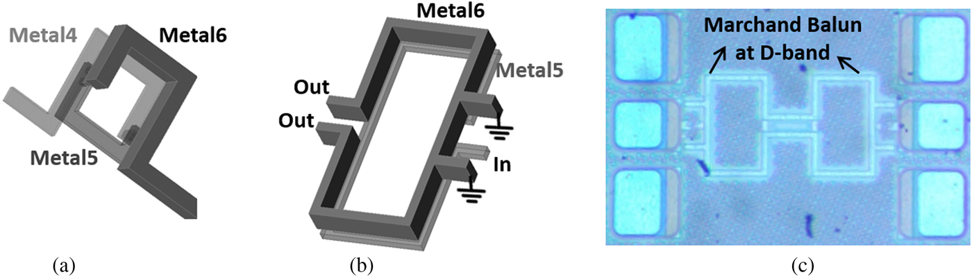
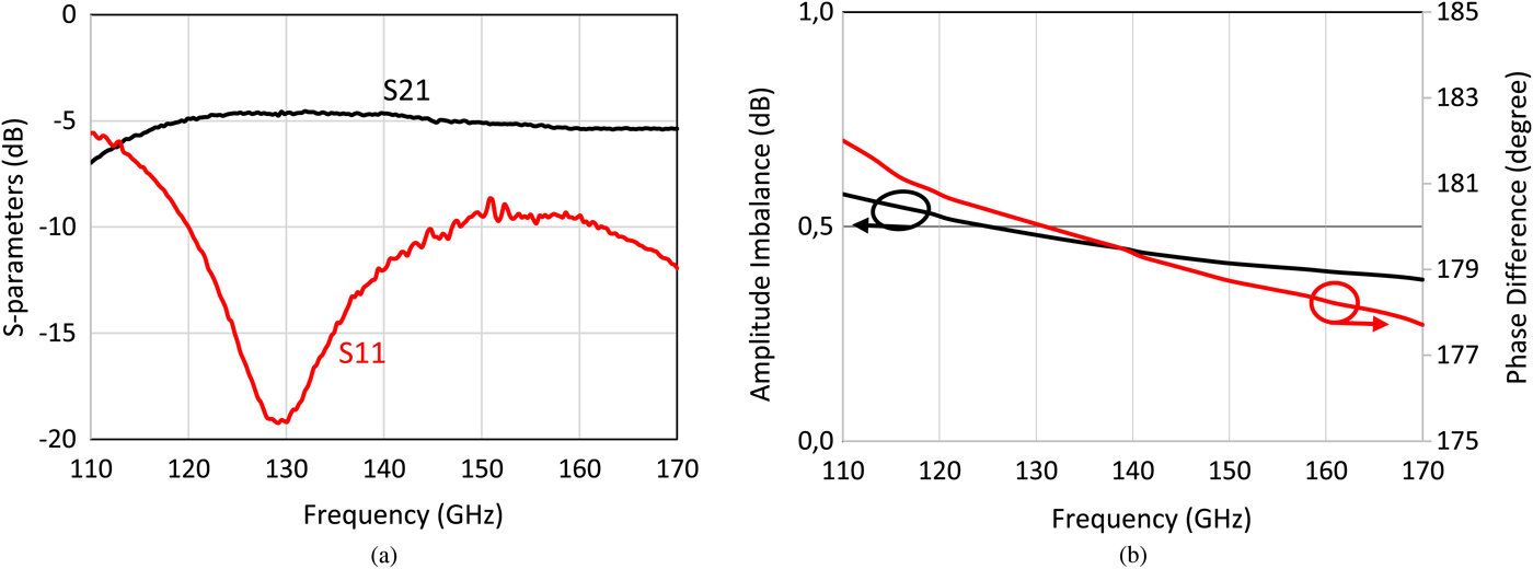
In order to minimize the sensitivity to noise and undesired couplings, single-ended signals are converted to differential as soon as they are interfaced to the chip. Single-ended to differential conversion is performed using Marchand baluns with broadside coupled lines on Metal6 and Metal5 layers, as shown in Fig. 1(b). Balanced signal lines are on Metal6, while Metal2 is still present as a dc return path and also to have a well-defined ground reference for common-mode signals. The same balun design is used on both LO and RF ports since these signals are at the same frequency for direct-conversion transmitter and receiver architectures. Figure 2(b) shows the simulated performance of the balun, indicating phase imbalance of 4° and amplitude imbalance of 0.57 dB over the D-band. The measured s-parameters of back-to-back connected Marchand baluns testing structure is shown in Fig. 2(a) and chip photo is presented in Fig. 1(c). The insertion loss is 4 ± 0.5 dB from 118 to 170 GHz and input return loss is better than 9 dB.
(a) Measured insertion loss of back-to-back connected Marchand baluns. (b) Simulated amplitude imbalance and phase difference between output ports of Marchand balun.
The particular topology of a quadrature-balanced mixer requires generation and distribution of differential 90° phase-shifted mmWave signals. Quadrature differential LO signals are generated with an on-chip differential coupler and are a differential implementation of the backward coupler [Reference Pozar19]. The coupler has 1.1 dB amplitude and 5° phase imbalance between the two output ports in the D-band. The reflection coefficients on input and output ports are simulated lower than 18 dB.
Quadrature modulator
Circuit design
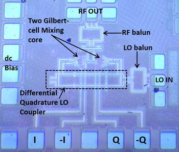
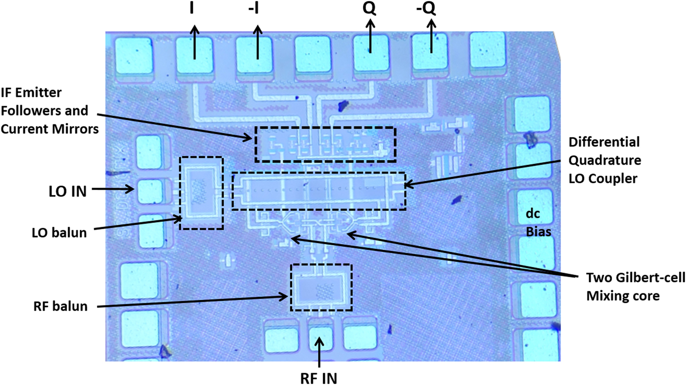
The block diagram of the I/Q modulator is shown in Fig. 3(a). The circuit consists of two Gilbert-cell mixers, an on-chip integrated differential quadrature LO coupler, and RF Marchand balun. The Gilbert-cell configuration provides high isolation between all three ports, as well as suppression of unwanted (spurious) mixing products at the output in a very compact die footprint [Reference Maas20]. For quadrature operation, the 90° phase shifter can be used either on the LO or the RF path. In the presented design, the phase shifter is inserted in the LO path for minimum noise figure. Figure 3(b) shows the schematic of the presented circuit. The input baseband signals are converted to current signals by the differential transconductance stage (T 9–T 10, T 11–T 12) and are fed to the differential pair (T 1–T 4, T 5–T 8) which is also called switching quads. The up-converted RF differential output currents are added and passed through a common inductive load (L 1). These two outputs are then connected to a balun for the differential to single-ended output conversion. A current mirror was included to control the currents in the mixer.
(a) Block diagram. (b) Schematic diagram of the quadrature modulator.

For optimal performance, the switching quad transistors are chosen 2 µm long and the transconductance transistors are accordingly scaled to 4 µm long. The larger device allows for higher current swings and therefore increased linearity. The baseband input ports are dc coupled. Decoupling capacitors (C d) are incorporated to avoid potential odd mode instability of the circuit. The chip photograph is shown in Fig. 4. In order to minimize any unwanted parasitic effects and to maintain the amplitude and phase balance of the modulator, the signal paths of the RF, LO, and IF were laid out as symmetric as possible. The LO coupler and matching networks are compact and symmetrically laid out around the mixer cells. The mixer collector is biased at + 2.8 V and takes 16 mA current. The LO and IF bias voltages are + 2 V (V LO) and + 1.7 V (V IF) as shown in Fig. 3(b).
Chip photograph of the quadrature modulator. The active chip size including the RF/LO baluns and the LO hybrid is 620 µm×480 µm.

Measurement setup and circuit characterization
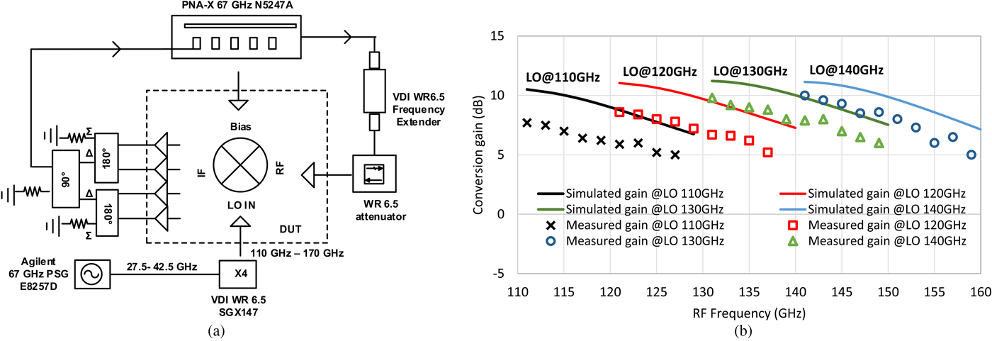
On-wafer probe measurements have been performed to characterize the I/Q modulator as a single sideband up-converting mixer using WR 6.5 waveguide GSG probes for the LO and RF ports and a GSSGSSG coaxial probe for the balanced IF ports. For the demonstration of single side-band operation, a CW signal with balanced four phases is applied to the differential I and Q ports. The LO signal is provided from an Agilent 8257D synthesizer together with VDI 6.5×4 multiplier chain. The LO power (measured with an Erikson power meter) after considering probe loss is between 4 and 7.5 dBm in the D-band. Details of the measurement setup are shown in Fig. 5(a). A Keysight PNA-X N5247A network analyzer with VDI WR 6.5 frequency extension module at RF port is used in the measurement. The losses due to probe, cable and hybrid network in measurement setup were calibrated and de-embedded in the presented data. The measured upper (USB) and lower (LSB) sideband conversion gains versus IF frequency at 126 GHz LO are shown in Fig. 6(a). The output power at 1 dB compression point was measured over the RF frequency (Fig. 5(b)) and has maximum output P 1dB of −4 dBm at 140 GHz output. The input signal power to both the I and Q ports are −27 dBm. The mixer exhibits up to 9.8 dB conversion gain and 19 dB image rejection ratio (IRR). The measured 3-dB IF bandwidth of the chip is 13 GHz which is in good agreement with the simulation. Figure 6(b) shows the simulated and measured USB conversion gain versus LO frequency at 1 GHz IF. The 3-dB RF bandwidth is 33 GHz from 119 to 152 GHz. Figure 6(c) shows the measured and simulated conversion gain versus input power at 1 GHz IF and 131 GHz RF. The input P 1dB is −14 dBm and can provide an output power of −2 dBm in saturation. For 1 GHz IF input, Fig. 5(b) shows the output power at 1-dB compression point over RF frequency in D band. The output P 1dB is −4 dBm at 140 GHz RF and 1 GHz IF. The LO signal power at the output port of mixer is measured. The 114 GHz LO signal power at RF port is −24 dBm which provides an LO-to-RF port isolation of 31 dB.
(a) The CW measurement setup of the I/Q modulator. (b) Measured output P 1dB versus RF frequency at 1 GHz IF.

(a) Conversion gain versus IF frequency at 126 GHz LO. (b) Conversion gain versus LO frequency at 1 GHz IF. (c) Conversion gain versus input power at 1 GHz IF and 131 GHz RF.

Quadrature demodulator
Circuit design and layout consideration
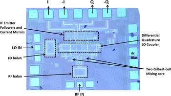
The schematic of the presented direct quadrature demodulator is shown in Fig. 7. The principle of operation of the demodulator circuit is similar to the modulator circuit. As shown in the chip photograph in Fig. 8, most parts of the circuit layout are also reused. The input RF signal is converted to a differential form with the Marchand balun and then divided to each mixer cells. The transconductance stage consisting of T 9–T 10 and T 11-T 12 transistors convert the RF input voltage signal into a current. This current then passes through switching transistor pairs (T 1–T 4 and T 5–T 8) which change the polarity of the current in every LO cycle. The low-frequency content of the resulting current signal is converted to voltage again by passing through resistive loads. The bias network on the bases of switching transistors maximizes the base-emitter voltage swing for effective switching. The emitter lengths of the switching transistors are chosen 2 µm for fast switching and transconductance stage transistors are accordingly scaled to 4 µm long for better linearity and current handling.
Schematic diagram of the quadrature demodulator circuit.

Chip photograph of the demodulator chip. The active chip size is 620 μm × 480 µm, including the RF/LO baluns and the LO hybrid.
The RF port is impedance matched to 50 Ω for interfacing to a low-noise amplifier or the antenna directly. Resistive IF loads are used to avoid the need for large on-chip inductors and to minimize the risk of instability. IF ports are isolated from the next stage by emitter followers (T 13–T 16), which are also biased by current sources and are designed to match to 50 Ω over a broadband. The IF interface is kept differential because most of the operational amplifiers have a differential input. If single ended termination is desired, one of the two outputs can be terminated, or alternatively, an external balun could be used.
The operating condition is set by the reference current, which is mirrored to two mixer cells, as shown in Fig. 7. The collector voltage of 2.8 V is applied to two mixing cells and to the four emitter followers, where mixer cells draw 8.5 mA and emitter followers draw 14 mA of current. Applied voltages to the bases of switching and transconductance transistors are 2.5 and 1.6 V, respectively.
Measurement setup and circuit characterization
On-wafer probe measurements have been performed to characterize the quadrature demodulator as an image-reject down-converting mixer. The experimental set up for continuous wave (CW) measurement is demonstrated in Fig. 9(a). A Keysight PNA-X N5247A network analyzer with VDI WR 6.5 frequency extension module at RF port is used to provide the RF signal in the D-band. A D-band variable attenuator is used to control the RF power to the circuit. The LO signal is generated by a VDI WR 6.5×4 multiplier chain. The four outputs from the demodulator are connected to three external hybrids through the IF probe. The single-sideband (SSB) conversion gain is measured at an RF power of −28 dBm to ensure linear operation of the circuit. The mixer is characterized at multiple LO frequencies across the D-band.
(a) CW measurement setup of the quadrature demodulator. (b) Conversion gain versus RF frequency at different LO frequencies.
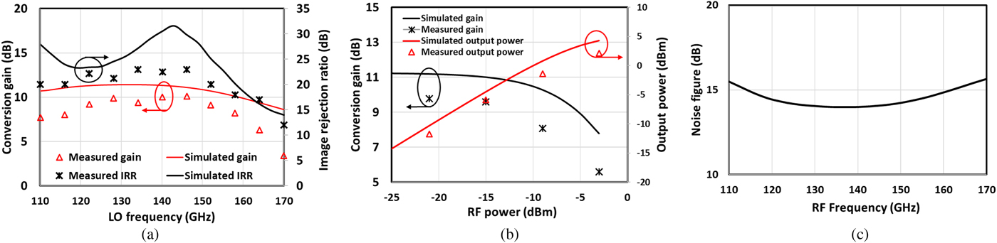
At different LO frequencies RF frequency is varied and USBs at the output are measured. Figure 9(b) presents the comparison between measured and simulated conversion gain. The modulator demonstrates a maximum conversion gain of 10 dB at 140 GHz LO and 141 GHz RF. The 3-dB variation in gain is measured over 18 GHz IF bandwidth. The RF frequency in D-band is swept with LO frequency to have a fixed IF of 1 GHz. At each RF frequency, the LO frequency is switched to above and below the RF in order to measure conversion gain in both LSB and USB. The ratio of the two output powers (IRR) is measured. An optimum collector current is observed for maximum image rejection, and as the current in mixing core increases, conversion gain increases. Measured conversion gain and image rejection versus LO frequency are shown and compared with simulated results in Fig. 10(a). A relatively flat gain response is obtained, with a maximum variation of 5 dB over an RF bandwidth of 110–165 GHz. The 3-dB RF bandwidth extends over 36 GHz from 117 to 153 GHz and the IRR is always better than 18 dB across most of the D-band and peaks to as high as 10 dB around 135 GHz LO frequency. Figure 10(b) demonstrates conversion gain and output power at 1 GHz versus input power at 138 GHz. The input P 1dB is −10 dBm and can provide up to 3 dBm of output power in saturation. The simulated SSB noise figure versus RF frequency is shown in Fig. 10(c) and varies from 14 to 16 dB in the complete D-band.
(a) Measured conversion gain and image rejection ratio versus LO frequency at 1 GHz IF. (b) Measured conversion gain and output power at 1 GHz versus RF power at 138 GHz. (c) Simulated SSB noise figure versus RF frequency at 1 GHz IF.
Data transmission measurement
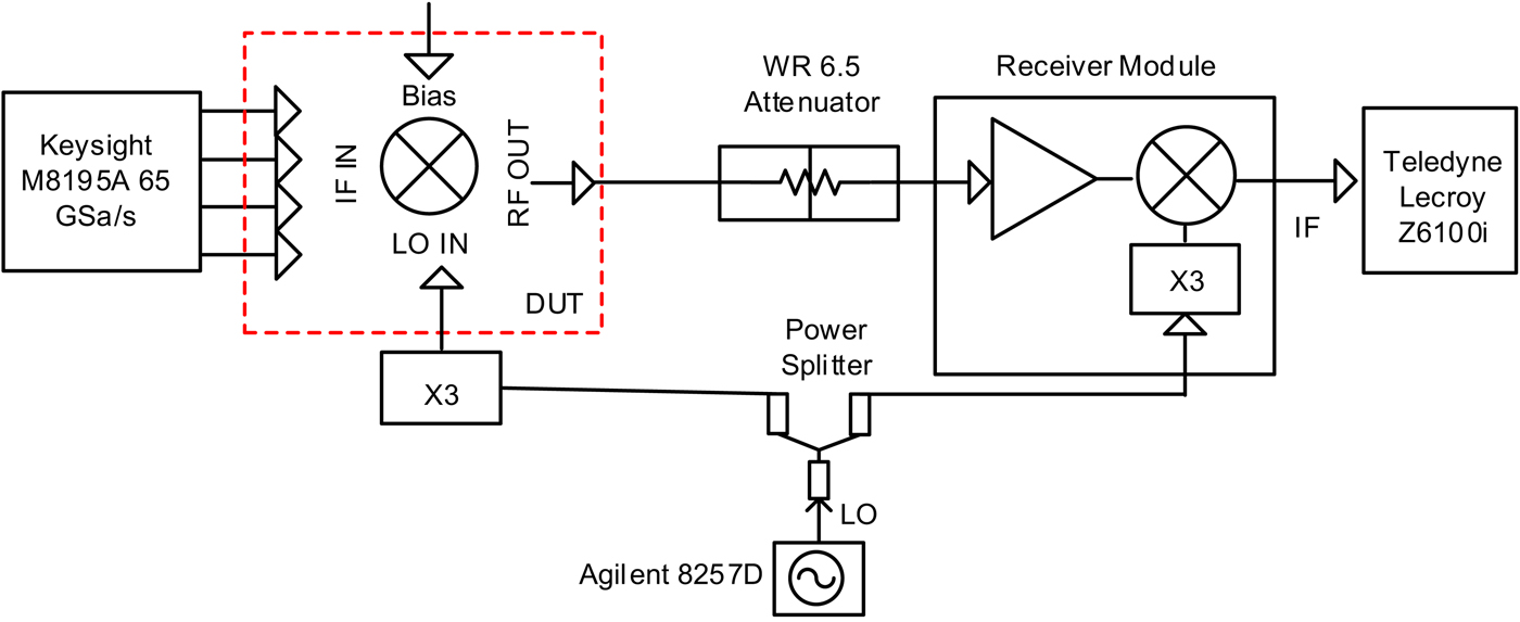
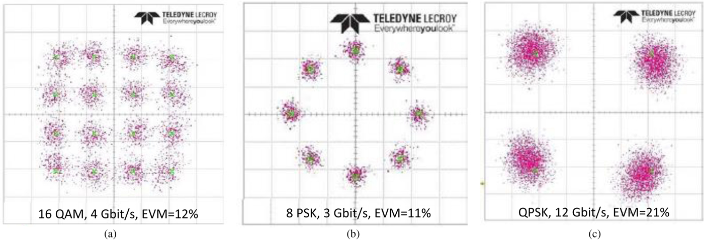
Data transmission is verified with the experimental setup as shown in Fig. 11. The modulator MMIC is probed on-wafer and an in-house developed D-band receiver is used at the receiver side [Reference Carpenter, Nopchinda, Abbasi, He, Bao, Eriksson and Zirath13]. The I/Q modulator and I/Q receiver are used as an SSB up-converting mixer and image reject receiver, respectively. An Arbitrary Waveform Generator (Keysight M8195A 65 GSa/s) is used to generate high-order QAM signals centered at 5 GHz IF. The generated signal is fed to the modulator which up-converts the IF input signal to RF at 131 GHz. A variable attenuator is inserted between the modulator and receiver in order to attenuate the RF signal to the receiver preventing the receiver to saturate. The receiver down-converts the incoming RF signal to IF before sampling by a real-time oscilloscope (Lecroy) with a fixed 80-G Samples/s sampling rate. Lecroy VSA software is used for demodulation and constellation analysis. Figure 12(a)–(c) shows constellation diagram for 16 QAM, 8PSK, and QPSK, respectively. A 12 Gbit/s QPSK data transmission using 131-GHz carrier signal is demonstrated on modulator with measured modulator-to-receiver error vector magnitude of 21%.
Experimental setup for data transmission test.
Received signal constellation diagram of (a) 4 Gbit/s 16QAM, (b) 3 Gbit/s 8PSK, and (c) 12 Gbit/s QPSK.
Performance summary and conclusion
A fully integrated multifunctional D-band direct I/Q modulator/demodulator circuit for mmWave applications is designed, fabricated, and verified experimentally. The circuits are fabricated using a commercial 130 nm SiGe BiCMOS process and can be used in both homodyne and heterodyne architectures. Tables 1 and Table 2 summarize the performance of this work with some recently published results in the similar frequency range. The modulator measured 3-dB RF bandwidth extends beyond 33 GHz from 119 to 152 GHz and the 3-dB IF bandwidth is 13 GHz. A maximum conversion gain of 9.8 dB is measured and has an input P 1dB of −14 dBm at 131 GHz RF and 1 GHz IF. The demodulator exhibits 10 dB conversion gain with 3-dB RF and IF bandwidths of 36 GHz (from 117 to153 GHz) and 16 GHz, respectively. It can nevertheless be seen that the presented designs demonstrate outstanding performance in terms of conversion gain, and RF/IF bandwidth for the given technology. The active area of each circuit including the RF/LO baluns and the LO hybrid is 620 µm × 480 µm. The dc power consumption of modulator and demodulator are 53 and 69 mW, respectively. The quadrature modulator and demodulator can be further integrated with LO multiplier and amplifier circuits to implement complete transceivers with multi-level QAM capability for high data rate communication.
Performance comparison of up-converting mixers

Performance comparison of down-converting mixers

Acknowledgements
Infineon Technologies, Villach, Austria is acknowledged for fabricating the circuit. This project has received funding from the European Union's Horizon 2020 research and innovation program under grant agreement no. 644039.
 Sona Carpenter (GSM'13) received the M.E. (Hons.) degree in Electronics and Telecommunication from the S. G. S. Institute of Technology and Science, Indore, India, in 2008, and is currently working toward the Ph.D. degree at Chalmers University of Technology, Goteborg, Sweden. In 2007, she joined the Satellite Payload Technology Area, Indian Space Research Organization, Ahmedabad, India, where she was a Scientist/Engineer involved with research and development of microwave circuits and subsystems for the Indian national and geostationary communication satellite pay load receivers. She is currently with the Microwave Electronic Laboratory, Chalmers University of Technology. Her current research interests include the design of millimeter-wave integrated circuits and systems with a focus on millimeter-wave high-speed wireless communication. She was a recipient of the 2013 GaAs Association Ph.D. Student Fellowship Award.
 Zhongxia Simon He (M'09) received the M.Sc. degree from Beijing Institute of Technology, Beijing, China, and the Ph.D. degree from Chalmers University of Technology, Göteborg, Sweden, in 2008 and 2014, respectively. He is currently an Assistant Professor with the Microwave Electronics Laboratory, Department of Microtechnology and Nanoscience (MC2), Chalmers University. His current research interests include high data rate wireless communication, modulation and demodulation, mixed-signal integrated circuit design, radar, and packaging.
 Herbert Zirath (M’ 86–SM'08–F'11) was born in Göteborg, Sweden, on 20 March 1955. He received the M.Sc. and Ph.D. degrees in Electrical Engineering from Chalmers University, Göteborg, Sweden, in 1980 and 1986, respectively. From 1986 to 1996 he was a researcher at the Radio and Space Science at Chalmers University, engaged in developing a GaAs and InP-based HEMT technology, including devices, models, and circuits. In the spring–summer 1998, he was a research fellow at Caltech, Pasadena, USA, engaged in the design of MMIC frequency multipliers and Class E Power Amplifiers. He is since 1996 Professor in High-Speed Electronics at the Department of Microtechnology and Nanoscience, MC2, at Chalmers University. He became the head of the Microwave Electronics Laboratory 2001. At present, he is leading a group of approximately 40 researchers in the area of high-frequency semiconductor devices and circuits. His main research interests include MMIC designs for wireless communication and sensor applications based on III-V, III-N, Graphene, and silicon devices. He is author/co-author of more than 570 refereed journal/conference papers, h-index of 37, and holds five patents. He is a research fellow at Ericsson AB, leading the development of a D-band (110–170 GHz) chipset for high data rate wireless communication. He is a co-founder of Gotmic AB, a company developing highly integrated frontend MMIC chip-sets for 60 GHz and E-band wireless communication.