





1 Introduction
Modelling plasma dynamics typically involves operating with classical fields on fine grids. This requires dealing with large amounts of data, especially in kinetic models, which are notorious for being computationally expensive. Quantum computing (QC) has the potential to significantly speed up kinetic simulations by leveraging quantum superposition and entanglement (see Nielsen & Chuang Reference Nielsen and Chuang2010). However, quantum speedup is possible only if the depth of a quantum circuit modelling the plasma dynamics scales advantageously (polylogarithmically) with the system size (number of grid cells). Achieving such efficient encoding is challenging and remains an open problem for most plasma systems of practical interest.
Here, we explore the possibility of an efficient quantum algorithm for modelling of linear oscillations and waves in a Vlasov plasma (see Stix Reference Stix1992). Previous works in this area focused on modelling either spatially monochromatic or conservative waves within initial-value problems (see Engel, Smith & Parker Reference Engel, Smith and Parker2019; Ameri et al. Reference Ameri, Ye, Cappellaro, Krovi and Loureiro2023; Toyoizumi, Yamamoto & Hoshino Reference Toyoizumi, Yamamoto and Hoshino2023). However, typical practical applications (for example, for magnetic confinement fusion) require modelling of inhomogeneous dissipative waves within boundary-value problems, which require different approaches. Here, we consider a minimal problem of this kind to develop a prototype algorithm that would be potentially extendable to such practical applications.
Specifically, we assume a one-dimensional collisionless Maxwellian electron plasma governed by the linearized Vlasov–Ampère system. Added to this system is a spatially localized external current (antenna) that drives plasma oscillations at a fixed frequency $\omega$ . This source produces evanescent waves if $\omega$
 is smaller than the plasma frequency $\omega _p$
 . For $\omega > \omega _p$
 , it produces Langmuir waves, which propagate away from the source while experiencing Landau damping along the way. Outgoing boundary conditions are adopted to introduce irreversible dissipation. This relatively simple system captures paradigmatic dynamics typical for linear kinetic plasma problems and, thus, can serve as a testbed for developing more general algorithms of practical interest. We start by showing how this system can be cast in the form of a linear vector equationFootnote 1

where $\boldsymbol {A}$ is a (non-Hermitian) square matrix, ${\boldsymbol{\psi} }$
 is a vector that represents the dynamical variables (the electric field and the distribution function) on a grid and $\boldsymbol {b}$
 describes the antenna. There is a variety of quantum algorithms that can solve equations like (1.1), for example, the Harrow–Hassidim–Lloyd algorithms (see Harrow, Hassidim & Lloyd Reference Harrow, Hassidim and Lloyd2009), the Ambainis algorithm (see Ambainis Reference Ambainis2012), the algorithms inspired by the adiabatic QC (see Costa et al. Reference Costa, An, Sanders, Su, Babbush and Berry2021; Jennings et al. Reference Jennings, Lostaglio, Pallister, Sornborger and Subaşı2023) and solvers based on the quantum signal processing (QSP) (see Low & Chuang Reference Low and Chuang2017, Reference Low and Chuang2019; Gilyén et al. Reference Gilyén, Su, Low and Wiebe2019; Martyn et al. Reference Martyn, Rossi, Tan and Chuang2021), to name a few. Here, we propose to use a method based on the QSP, specifically, the quantum singular value transformation (QSVT) (see Gilyén et al. Reference Gilyén, Su, Low and Wiebe2019; Martyn et al. Reference Martyn, Rossi, Tan and Chuang2021), because it is known to scale near optimally with the condition number of $\boldsymbol {A}$
 and the desired precision.
Specifically, this paper focuses on the problem that one unavoidably has to overcome when applying the QSVT to kinetic plasma simulations. This problem is how to encode the corresponding large-dimensional matrix $\boldsymbol {A}$ into a quantum circuit. A direct encoding of this matrix is prohibitively inefficient. Various methods for encoding matrices into quantum circuits were developed recently (see Clader et al. Reference Clader, Dalzell, Stamatopoulos, Salton, Berta and Zeng2022; Camps et al. Reference Camps, Lin, Beeumen and Yang2023; Zhang & Yuan Reference Zhang and Yuan2023; Kuklinski & Rempfer Reference Kuklinski and Rempfer2024; Lapworth Reference Lapworth2024; Liu et al. Reference Liu, Du, Lin, Vary and Yang2024; Sünderhauf, Campbell & Camps Reference Sünderhauf, Campbell and Camps2024). We propose how to make it more efficiently by compressing the content of $\boldsymbol {A}$
 at encoding. The same technique can be applied in modelling kinetic or fluid plasma and electromagnetic waves in higher-dimensional problems, so our results can be used as a stepping stone towards developing more practical algorithms in the future. The presentation of the rest of the algorithm and (emulation of) quantum simulations are left to future work.
Our paper is organized as follows. In § 2 we present the main equations of the electrostatic kinetic plasma problem. In § 3 we present the numerical discretization of this model. In § 4 we cast the discretized equations into the form (1.1). In § 5 we present classical numerical simulations of the resulting system, which can be used for benchmarking quantum algorithms. In § 6 we present the general strategy for encoding the matrix $\boldsymbol {A}$ into a quantum circuit. In § 7 we explicitly construct the corresponding oracle and discuss how it scales with the parameters of the problem. In § 8 we present a schematic circuit of the quantum algorithm based on this oracle. In § 9 we present our main conclusions.
2 Model
2.1 One-dimensional Vlasov–Ampère system
Electrostatic oscillations of a one-dimensional electron plasma can be described by the Vlasov–Ampère system


where $E(t, x)$ is the electric field, $f(t, x, v)$
 is the electron probability distribution, $t$
 is time, $x$
 is the coordinate in the physical space, $v$
 is the coordinate in the velocity space, $e > 0$
 is the elementary charge and $m_e$
 is the electron mass. We have also introduced a fixed source term $\mathcal {F} = \mathcal {F}(x, v)$
 (balanced by particle losses through the plasma boundaries), which is explained below. The term $j^{(S)}$
 represents a prescribed source current that drives plasma oscillations. The corresponding source charge density $\rho ^{(S)}$
 can be inferred from $j^{(S)}$
 using the charge conservation law

Let us split the electron distribution into the background distribution $F$ and a perturbation $g$
 :
:

We assume that $g$ is small, so the system can be linearized in $g$
 . Also, because we assume a neutral plasma, the system does not have a background electric field, so the stationary background distribution satisfies $v\partial _x F = \mathcal {F}$
 . Provided that $\mathcal {F}$
 depends on $x$
 , $F$
, $F$ can be spatially inhomogeneous. At the same time, since $\mathcal {F}$
 is fixed, it does not enter the equation for $g$
 . This leads to the following linearized equations:Footnote 2

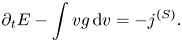
Here, $v$ is normalized to $v_{\rm th}$
 , $x$
, $x$ is normalized to the electron Debye length $\lambda _D$
 and the time is normalized to the inverse electron plasma frequency $\omega _{p}^{-1}$
 , where

where $n_{\rm ref}$ and $T_{\rm ref}$
 are some fixed values of the electron density and temperature, respectively. The distribution functions $g$
 and $F$
 are normalized to $n_{\rm ref}/v_{\rm th}$
 , and $E$
 is normalized to $T_{\rm ref}/(e\lambda _D)$
 . We also assume that $F$
 is Maxwellian, i.e.

where the background density $n$ and temperature $T$
 are normalized to $n_{\rm ref}$
 and $T_{\rm ref}$
 , respectively. An analytical description of the system (2.4) is presented in Appendix A.
2.2 Boundary-value problem
To reformulate (2.4) as a boundary-value problem, we consider a source oscillating at a constant real frequency $\omega _0$ :
:

Assuming $g, E \propto \exp (-\mathrm {i}\omega _0 t)$ , one can recast (2.4) as

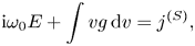
where $H = F/T$ and the variables $g$
 and $E$
 are now considered as the corresponding time-independent complex amplitudes. For definiteness, we impose a localized current source:

Then, by (2.2), the corresponding charge density is that of an oscillating dipole:

We will be interested in the spatial distribution of the electric field $E(x)$ driven by the source $j^{(S)}$
 and undergoing linear Landau damping caused by interaction of this field with the distribution perturbation $g$
 .
.
To avoid numerical artifacts and keep the grid resolution reasonably low, we impose an artificial diffusivity $\eta$ in the velocity space by modifying (2.8a) as

This allows us to reduce the grid resolution in both velocity and real space.
To avoid numerical errors caused by the waves reflected from spatial boundaries, we impose outgoing (non-reflecting) boundary conditions on both edges (see Thompson Reference Thompson1987). The resulting system is

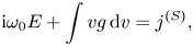
where
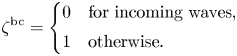
In our case of a one-dimensional system, the incoming waves correspond to $v < 0$ at the right spatial boundary of the simulation box and $v > 0$
 at the left spatial boundary.
3 Discretization
To discretize (2.12), we introduce the spatial grid

and the velocity grid

Here, $q_x = N_x-1$ and $q_v = N_v-1$
 , where

For convenience, we also introduce the integer $M_v = 2^{n_v-1}$ . The first $M_v$
 points on the velocity grid, $k=[0,M_v)$
 , correspond to $v_k < 0$
 , and the last $M_v$
 points, $k=[M_v,N_v)$
 , correspond to $v_k > 0$
 . The notation $[k_1,k_2)$
 , where $k_1$
 and $k_2$
 are integers, denotes the set of all integers from $k_1$
 to $k_2$
 , including $k_1$
 but excluding $k_2$
 . Similarly, the notation $[k_1,k_2]$
 denotes the set of integers from $k_1$
 to $k_2$
 , including both $k_1$
 and $k_2$
 . Also, throughout this paper, the discretized version of any given function $y(x,v)$
 is denoted as $y_{j,k}$
 , where the first subindex is the spatial-grid index and the second subindex is the velocity-grid index
The integral in the velocity space is computed by using the corresponding Riemann sum, $\int y(v)\,{\rm d} v = \sum _k y(v_k)\Delta v$ . To remove $\Delta v$
 from discretized equations, we renormalize the distribution functions as

In real space, we use the central finite difference scheme



where $\sigma = (2h)^{-1}$ , $j = [1,N_x-2]$
 , $k=[0,N_v)$
 and the expressions for the derivatives at the boundaries are obtained by considering the Lagrange interpolating polynomial of the second order. (Instead of using the diffusivity $\eta$
 introduced in (2.11) to smooth high-frequency oscillations in phase space, it might be possible to apply the upwinding difference scheme that is often used for the discretization of convective equations; see, for example, Brio & Wu Reference Brio and Wu1988.) Similarly, the second derivative with respect to velocity is discretized as



where $\beta = \Delta v^{-2}$ , $j = [0,N_x)$
 , $k=[1,N_v-2]$
 and the derivatives at the boundaries are obtained by considering the Lagrange polynomial of the third order.
After the discretization, the Vlasov equation (2.12a) becomes

where $j = [0,N_x)$ and $k=[0,N_v)$
 . The function $P_{j,k}$
 is given by

where $\delta _{k_1,k_2}$ is the Kronecker delta:
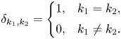
The function $p^{\rm sign}_k = 1 - 2(\delta _{k,0}+\delta _{k,q_v})$ appears because the discretization (3.6) in velocity results in different signs in front of the diagonal element $g_{j,k}$
 for bulk and boundary velocity elements. The coefficient $(\delta _{j,0}-\delta _{j,q_x})$
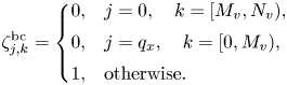
 is necessary to take into account the different signs that appear due to the discretization in space (3.5) at bulk and boundary points. The function $\zeta ^{\rm bc}_{j,k}$
 is the discretized version of the function (2.13) responsible for the outgoing boundary conditions:
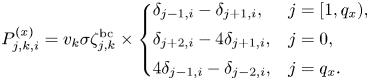
The function $P^{(x)}_{j,k,i}$ varies for bulk and boundary spatial points according to (3.5):
The function $P^{(v)}_{i,k}$ varies for bulk and boundary velocity points according to (3.6):

Finally, Ampère's law (2.12b) is recasted as
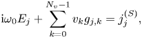
where $j=[0,N_x)$ .
.
4 Matrix representation
After the discretization, (3.7) and (3.13) can be converted into the form of (1.1) as follows.
4.1 The vector ${\psi }$

First of all, to construct (1.1), one needs to encode $g_{j,k}$ and $E_j$
 into ${\boldsymbol{\psi} }$
 . Since one needs to store $N_f = 2$
 fields on a $N_x\times N_v$
 phase space, the size of ${\boldsymbol{\psi} }$
 should be $N_{\rm tot} = N_f N_{xv}$
 , where $N_{xv} = N_x N_v$
 , and this vector can be saved by using $1+n_x+n_v$
 qubits, where $n_x$
 and $n_v$
 have been introduced in (3.3a,b). Within the vector ${\boldsymbol{\psi} }$
 , the fields are arranged in the following way:
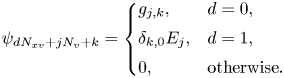
Here $\psi _{d N_{xv} + j N_v + k}$ are the elements of ${\boldsymbol{\psi} }$
 with $j = [0, N_x)$
 , $k = [0,N_v)$
 and $d = [0, N_f)$
 . Since the electric field does not depend on velocity, the second half of ${\boldsymbol{\psi} }$
 is filled with $E_j$
 only if the velocity index $k$
 is equal to zero.
To address each field, $g_{j,k}$ or $E_j$
 , we introduce the register $r_f$
 with one qubit. The zero state $\mid {0}\rangle_{r_f}$
 corresponds to addressing the plasma distribution function, and the unit state $\mid {1}\rangle_{r_f}$
 flags the electric field. We also use additional two registers, denoted $r_x$
 and $r_v$
 , with $n_x$
 and $n_v$
 qubits, respectively, to specify the fields’ position in the real and velocity spaces, correspondingly. Then, one can express the vector ${\boldsymbol{\psi} }$
 as
as

where $\eta _{\psi, {\rm norm}}$ is the normalization factor used to ensure that $\langle \psi |\psi \rangle = 1$
 . (The assumed notation is such that the least significant qubit is the rightmost qubit. In quantum circuits, the least significant qubit is the lowest one.) Notably, this encoding can be called half-analogue, since the electric field and the electron distribution function are encoded into the amplitudes of the quantum state, which is a continuous variable. However, positions in phase space are discretized and digital since they are encoded into bitstrings of the quantum states.
4.2 The source term
Corresponding to (4.1), the discretized version of the vector $\boldsymbol {b}$ in (1.1) is as follows:
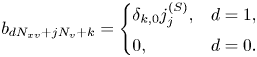
Note that all elements in the first half of $\boldsymbol {b}$ are zero, and, in its second half, only every $N_v$
 th element is non-zero. In the ‘ket’ notation, this can be written as

where $\eta _{b,{\rm norm}}$ is the normalization factor used to ensure that $\langle b|b \rangle = 1$
 .
.
4.3 The matrix ${A}$

The corresponding $N_{\rm tot}\times N_{\rm tot}$ matrix $\boldsymbol {A}$
 is represented as
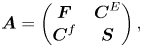
where $\boldsymbol {F}$ , $\boldsymbol {C}^E$
 , $\boldsymbol {C}^f$
 and $\boldsymbol {S}$
 are $N_{xv}\times N_{xv}$
 submatrices. A schematic structure of this matrix is shown in figure 1. The submatrix $\boldsymbol {F}$
 encodes the coefficients in front of $g$
 in the Vlasov equation (3.7) and is given by
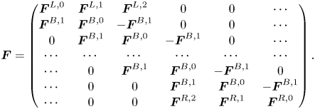
This submatrix consists of $N_x^2$ blocks, whose elements are mostly zeros. Each block is of size $N_v\times N_v$
 , and the position of each block's elements is determined by the row index $k_r = [0, N_v)$
 and the column index $k_c = [0, N_v)$
 . The discretization at the left spatial boundary is described by the blocks $\boldsymbol {F}^{L,0}$
 , $\boldsymbol {F}^{L,1}$
 and $\boldsymbol {F}^{L,2}$
 . The discretization at the right spatial boundary is described by the blocks $\boldsymbol {F}^{R,0}$
 , $\boldsymbol {F}^{R,1}$
 and $\boldsymbol {F}^{R,2}$
 . The discretization at the bulk spatial points is described by the blocks $\boldsymbol {F}^{B,0}$
 and $\boldsymbol {F}^{B,1}$
 . Using (3.8), (3.11) and (3.12), one obtains the following expressions for the elements in each block in (4.6) at the left spatial boundary:



At the right spatial boundary,



and at bulk spatial points,


We denote the part of the submatrix $\boldsymbol {F}$ that depends on $v$
 as $\tilde {\boldsymbol {F}}$
 . The matrix elements of $\tilde {\boldsymbol {F}}$
 are indicated in figure 1 with red. The part of $\boldsymbol {F}$
 that does not depend on $v$
 is denoted as $\hat {\boldsymbol {F}}$
 and shown in blue in figure 1 within the submatrix $\boldsymbol {F}$
 .
.


The matrix $\boldsymbol {C}^E$ is block diagonal and encodes the coefficients in front of $E$
 in the Vlasov equation (3.7):

Here $j_r,j_c = [0, N_x)$ and $k_r, k_c = [0,N_v)$
 . In this submatrix the first column in each diagonal block of size $N_v\times N_v$
 is non-sparse whilst all other columns are filled with zeros. The Kronecker delta $\delta _{k_c,0}$
 appears because of the chosen encoding of the electric field into the state vector ${\boldsymbol{\psi} }$
 according to (4.1).
The submatrix $\boldsymbol {C}^f$ is also block diagonal and encodes the coefficients in front of $g$
 in (3.13):

Here $j_r,j_c = [0, N_x)$ and $k_r, k_c = [0,N_v)$
 . The first row in each block of size $N_v\times N_v$
 is non-sparse due to the sum in (3.13).
Finally, the matrix $\boldsymbol {S}$ is diagonal and encodes the coefficients in front of $E$
 in (3.13):

Here $j_r,j_c = [0, N_x)$ and $k_r, k_c = [0,N_v)$
 .
.
5 Classical simulations
To test our discretization scheme, we performed classical simulations for homogeneous plasma ($n = T = 1$ ), which facilitates comparison with the analytic theory described in Appendix A. In our simulations, the phase space is described by $x_{\rm max} = 100, n_x = 9$
 and $v_{\rm max} = 4, n_v = 8$
 . The source in the form (2.9) is placed at $x_0 = 50$
 with $\varDelta _S = 1.0$
 . We consider two cases (figure 2): (a) $\omega _0 = 1.2$
 , which corresponds to the case when the source frequency exceeds the plasma frequency; and (b) $\omega _0 = 0.8$
 , which corresponds to the case when the plasma frequency exceeds the source frequency. The numerical calculations were performed by inverting the matrix (4.5) using the sparse-QR-factorization-based method provided in CUDA toolkit cuSOLVER (see Novikau Reference Novikau2024a; cuSolver 2024).
Plots showing the spatial distribution of the electric field computed numerically (blue) and analytically (red) using (A17). (a,c) Plots of ${\rm Re}\,E$ and ${\rm Im}\,E$
 , respectively, for $\omega _0 = 1.20$
 . One can see Langmuir waves propagating away from the source (located at $x = x_0$
 ) and experiencing weak Landau damping. (b,d) Plots of ${\rm Re}\,E$
 and ${\rm Im}\,E$
 , respectively, for $\omega _0 = 0.8$
 . One can see Debye shielding of the source charge. In both cases, $n_x = 9$
 , $n_v = 8$
 and $\eta = 0$
 .
.
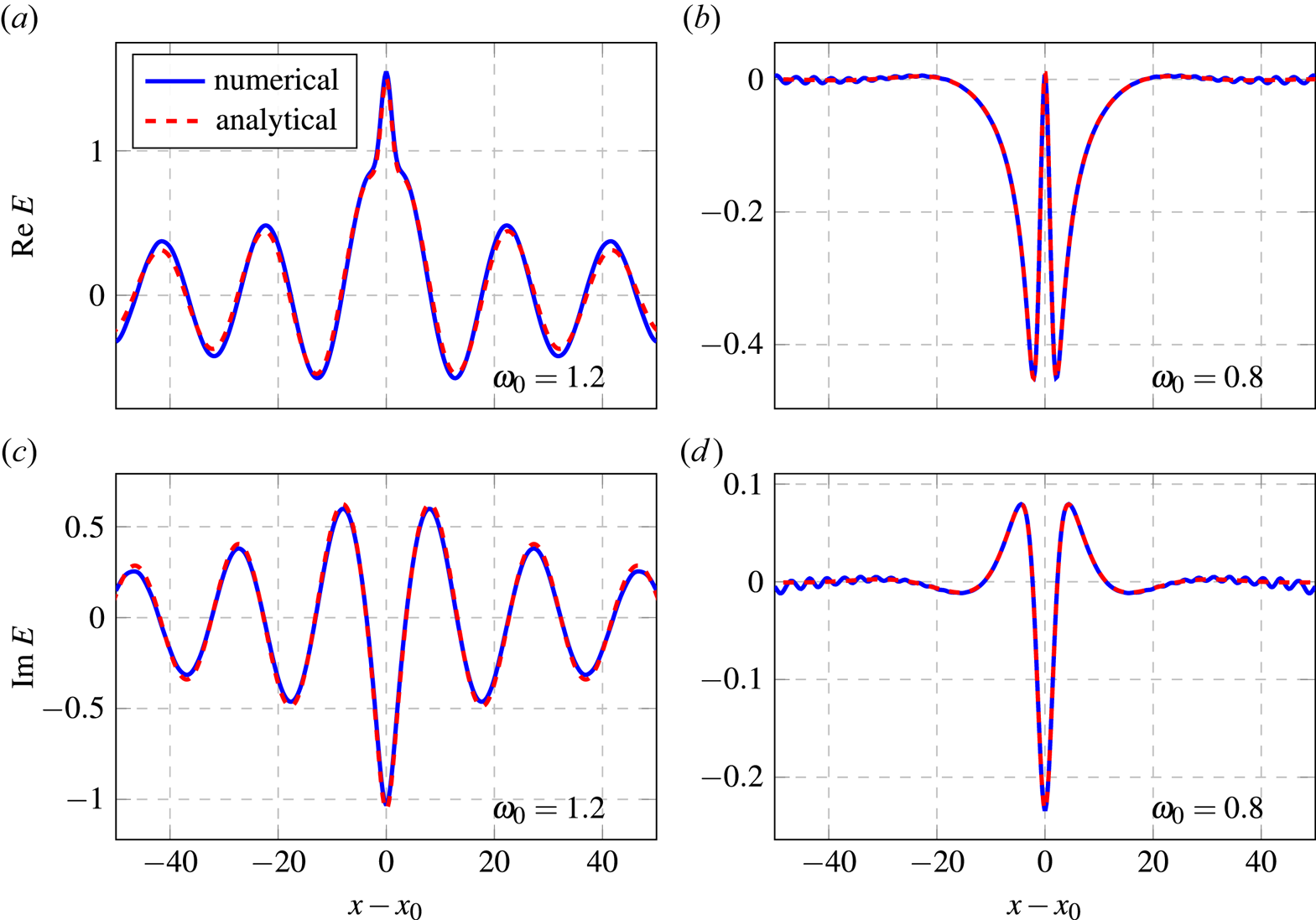
In the case with $\omega _0 = 1.2$ , the source launches Langmuir waves propagating outward and gradually dissipating via Landau damping. The outgoing boundary conditions allow the propagating wave to leave the simulated box with negligible reflection. In the case with $\omega _0 = 0.8$
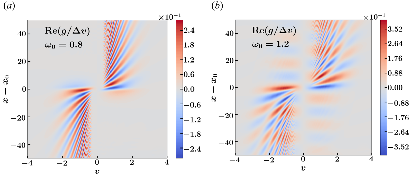
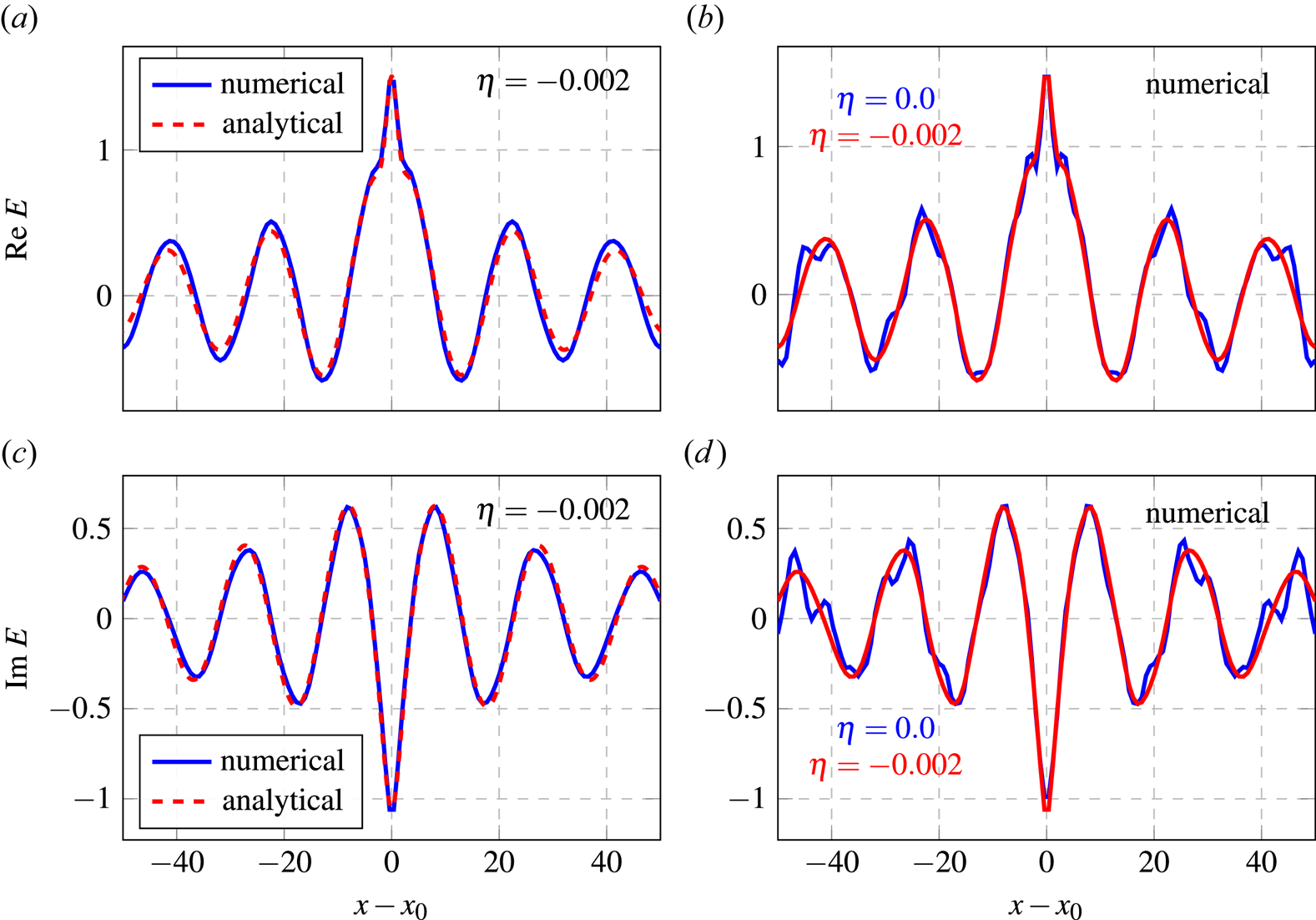
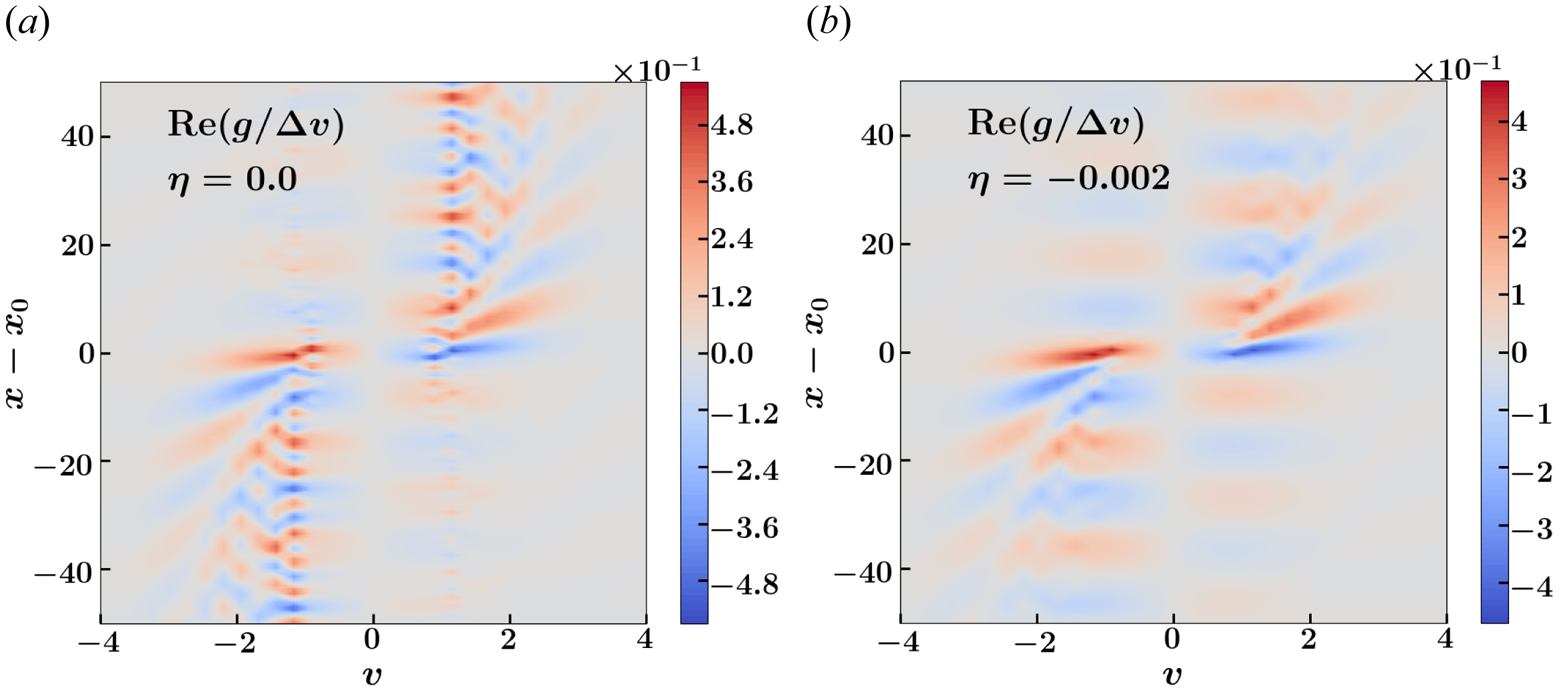
 , the plasma shields the electric field, which penetrates plasma roughly up to a Debye length. Due to the high resolution in both real and velocity space, the model remains stable and does not generate visible numerical artifacts (figure 3). Artifacts become noticeable at lower resolution (figures 4 and 5) but can be suppressed by introducing artificial diffusivity $\eta$
 in velocity space (2.11). Such simulations are demonstrated in figures 4 and 5 for $n_x = 7, n_v = 5$
 and $\eta = 0.002$
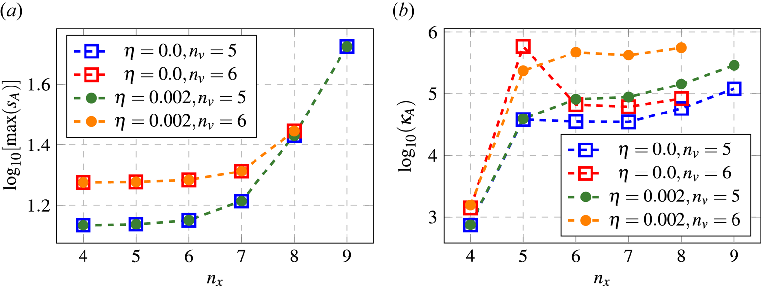
 . As seen in figure 4, the results are in good agreement with the analytical solution. The introduction of the diffusivity does not change the spectral norm of the matrix $\boldsymbol {A}$
 (figure 6a), which is always much higher than unity. However, keep in mind that the diffusivity complicates block encoding (BE) (§ 6.4) and somewhat increases the condition number $\kappa _A$
 of $\boldsymbol {A}$
 (figure 6b). The condition number grows with both $n_v$
 and $n_x$
 (except in cases with poor spatial resolution). In particular, if one takes $n_x = 7$
 , $n_v = 5$
 and $\eta = 0.002$
 , as in the simulations above, then $\kappa _A = 8.844\times 10^4$
 (i.e. $\log _{10}\kappa _A = 4.95$
 ). Without the diffusivity, and with the same phase-space resolution, the condition number is $\kappa _A = 3.489\times 10^4$
 (i.e. $\log _{10}\kappa _A = 4.54$
 ).
).
Plots showing the real component of the plasma distribution function, in units $\Delta v$ , computed numerically with $n_x = 9$
 , $n_v = 8$
 and $\eta = 0.0$
 . Results are shown for (a) $\omega _0 = 0.8$
 and (b) $\omega _0 = 1.2$
 .
.
Plots showing the spatial distribution of the electric field for $\omega _0 = 1.2$ , $n_x = 7$
 , and $n_v = 5$
 . (a,c) Results from the numerical (blue) and analytical (red) computations with the diffusivity $\eta = 0.002$
 . (b,d) Results from the numerical computations with (red) and without (blue) diffusivity.
Plots showing the real component of the plasma distribution function, in units $\Delta v$ , computed numerically for the cases with $\omega _0=1.2, n_x = 7$
 and $n_v = 5$
 . Results are shown for (a) $\eta = 0.0$
 and (b) $\eta = 0.002$
 .
.
Plots showing the dependence of the maximum singular value (a) and the matrix condition number (b) of the matrix $\boldsymbol {A}$ on the size of the spatial grid for various $\eta$
 and $n_v$
 . The values are computed numerically (Novikau Reference Novikau2024b).
6 Encoding the equations into a quantum circuit
6.1 Initialization
To encode the right-hand-side vector (4.4) into a quantum circuit, one can use the fact that the shape of the source current (2.9) is Gaussian. As shown in Novikau, Dodin & Startsev (Reference Novikau, Dodin and Startsev2023), Kane, Gomes & Kreshchuk (Reference Kane, Gomes and Kreshchuk2023) and Hariprakash et al. (Reference Hariprakash, Modi, Kreshchuk, Kane and Bauer2023), one can encode this function by using either QSVT (see Gilyén et al. Reference Gilyén, Su, Low and Wiebe2019; Martyn et al. Reference Martyn, Rossi, Tan and Chuang2021) or the so-called quantum eigenvalue transformation of unitaries (QETU) (see Dong, Lin & Tong Reference Dong, Lin and Tong2022), where the scaling of the resulting circuit is $\mathcal {O}(n_v \log _2(\varepsilon ^{-1}_{\rm qsvt}))$ and $\varepsilon _{\rm qsvt}$
 is the desired absolute error in the QSVT approximation of the Gaussian. However, one should keep in mind that the success probability of the initialization circuit depends on the Gaussian width. To increase this probability, amplitude amplification can be used (see Brassard et al. Reference Brassard, Høyer, Mosca and Tapp2002). After the initialization, the required initial state $\mid {b}\rangle$
 is usually entangled with the zero state of the ancillae used for the QSVT/QETU procedure and for the amplitude amplification. Thus, the subsequent QSVT circuit computing the inverse matrix $\boldsymbol {A}^{-1}$
 should be controlled by this zero state to guarantee that $\boldsymbol {A}^{-1}$
 acts on the state $\mid {b}\rangle$
 .
.
6.2 Block encoding: basic idea
To solve (1.1) with the matrix (4.5) and the source (4.4) on a digital quantum computer, one can use the QSVT, which approximates the inverse matrix $\boldsymbol {A}^{-1}$ with an odd polynomial of the matrix singular values. (The mathematical foundations of the QSVT are described, for example, in Gilyén et al. Reference Gilyén, Su, Low and Wiebe2019; Martyn et al. Reference Martyn, Rossi, Tan and Chuang2021; Lin Reference Lin2022.) The QSVT returns a quantum state $\mid {\psi _{\rm qsvt}}\rangle$
 whose projection on zero ancillae is proportional to the solution ${\boldsymbol{\psi} }$
 of (1.1):

Here $\phi _{\rm glob}$ is an unknown global angle and the scalar parameter $\kappa _{\rm qsvt}$
 is of the order of the condition number of the matrix $\boldsymbol {A}$
 .
.
A typical QSVT circuit is shown in figure 7, where the angles $\phi _i$ are computed classically. These angles serve as the parameters that specify the function computed by the QSVT circuit. In our case, the function is the inverse function. (More details about the computation of the QSVT angles can be found in Dong et al. Reference Dong, Meng, Whaley and Lin2021; Ying Reference Ying2022). The subcircuit $U_A$
 is the so-called BE oracle with the following matrix representation:
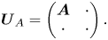
Here $\boldsymbol {U}_A$ is a unitary matrix. (The dots correspond to submatrices that keep $\boldsymbol {U}_A$
 unitary but otherwise are unimportant.) This unitary encodes the matrix $\boldsymbol {A}$
 as a sub-block that is accessed by setting the ancilla register ‘be’ to zero:

The QSVT addresses the BE oracle $\mathcal {O}(\kappa _{\rm qsvt}\log _2(\varepsilon ^{-1}_{\rm qsvt}))$ times to approximate the inverse matrix $\boldsymbol {A}^{-1}$
 . The efficient implementation of the BE oracle is the key to a potential quantum speedup that might be provided by the QSVT. As discussed in Novikau et al. (Reference Novikau, Dodin and Startsev2023), the QSVT can provide a polynomial speedup for two- and higher-dimensional classical wave systems if the quantum circuit of the BE oracle scales polylogarithmically or better with the size of $\boldsymbol {A}$
 .
.
The QSVT circuit encoding a real polynomial of order $N_a$ , where $N_a$
 is odd, by using $N_a + 1$
 angles $\phi _k$
 pre-computed classically. The gates denoted as $R_{z,k}$
 represent the rotations $R_z(2\phi _k)$
 . For an even $N_a$
 , the gate $Z$
 should be removed and the rightmost BE oracle $U_A$
 should be replaced with its Hermitian adjoint version $U_A^{\dagger}$
 .
.

To block encode a non-Hermitian matrix such as $\boldsymbol {A}$ , one can first extend it to a Hermitian one as
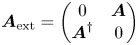
and then use the technique from Berry & Childs (Reference Berry and Childs2012). However, this will require at least two additional ancilla qubits for the extension (6.4). Another option is to decompose $\boldsymbol {A}$ into two Hermitian matrices, i.e.

where $\boldsymbol {A}_h = (\boldsymbol {A} + \boldsymbol {A}^{\dagger} )/2$ and $\boldsymbol {A}_a = (\boldsymbol {A} - \boldsymbol {A}^{\dagger} )/(2\mathrm {i})$
 . The sum (6.5) can be computed by using the circuit of linear combination of unitaries, which requires an additional ancilla. Also note that the matrices $\boldsymbol {A}_a$
 and $\boldsymbol {A}_h$
 , although being Hermitian, still have a non-trivial structure. Thus, for this method, it is necessary to block encode two separate matrices, which may double the depth of the BE oracle.
To reduce the number of ancillae and avoid encoding two matrices instead of one, we propose to encode the non-Hermitian $\boldsymbol {A}$ directly, without invoking the extension (6.4) or the splitting (6.5). This technique was already used in Novikau et al. (Reference Novikau, Dodin and Startsev2023). Although the direct encoding requires ad hoc construction of some parts of the BE oracle, this approach leads to a more compact BE circuit.
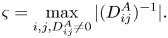
To encode $\boldsymbol {A}$ into the unitary $\boldsymbol {U}_A$
 , one needs to normalize $\boldsymbol {A}$
 such that $\varsigma ||\boldsymbol {A}||_{\rm max} \leq 1$
 , where
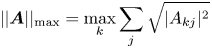
and $\varsigma$ is related to the matrix non-sparsity as will be explained later (see (6.14)). Here, by the term ‘non-sparsity’, we understand the maximum number of non-zero elements in a matrix row or column.Footnote 3 Hence, $\boldsymbol {A}$
 should be normalized as

The general structure of a BE oracle implementing the direct encoding of a non-Hermitian matrix is

where the oracles $O_F$ , $O^{F}_{F,{\rm corr}}$
 , $O_M$
 , $O^{B}_{F,{\rm corr}}$
 and $O^{\dagger} _F$
 encode the positions of non-zero matrix elements in $\boldsymbol {A}$
 , and $O_H$
 encodes the values of these elements. The upper superscripts ‘F’ and ‘B’ stand for ‘forward’ and ‘backward’ action. The oracle $U_A$
 can be constructed by using quantum gates acting on a single qubit but controlled by multiple qubits. Here, such gates are called single-target multicontrolled (STMC) gates (§ 6.3).
Equation (6.8) is based on the BE technique from Berry & Childs (Reference Berry and Childs2012) with the only difference that the oracles $O^{F}_{F,{\rm corr}}$ and $O^{B}_{F,{\rm corr}}$
 are introduced to take into account the non-Hermiticity of $\boldsymbol {A}$
 and are computed ad hoc by varying STMC gates. Basically, the oracles $O_F$
 , $O_M$
 and $O^{\dagger} _F$
 create a structure of a preliminary Hermitian matrix that is as close as possible to the target non-Hermitian matrix $\boldsymbol {A}$
 . The structure is then corrected by the oracles $O^{F}_{F,{\rm corr}}$
 and $O^{B}_{F,{\rm corr}}$
 constructed by varying their circuits to encode the structure of $\boldsymbol {A}$
 .
.
We consider separately the action of the oracle


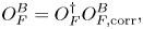
where the oracle $O_H$ is not included, and the oracles $O^{F}_F$
 and $O^{B}_F$
 are introduced to simplify notations. The matrix representation of the oracle $U_D$
 projected onto zero ancillae is denoted as $\boldsymbol {D}^A$
 . The matrix $\boldsymbol {D}^A$
 has non-zero elements at the same positions as those of the non-zero elements of $\boldsymbol {A}$
 .
.
We use the input register ‘in’ to encode a row index $i_r$ and the ancilla register $a_c$
 to perform intermediate computations. Then,

where $i_{c}$ are the column indices of all non-zero elements of $\boldsymbol {A}$
 at the row $i_r$
 ; $N_{c,i_r}$
 is the number of these elements at $i_r$
 ; $d_{i_r i_{c}} \leq 1$
 are the matrix elements of $\boldsymbol {D}^A$
 . The number $N_{c,i_r}$
 is less or equal to the non-sparsity of $\boldsymbol {A}$
 and can be different at different $i_c$
 . The elements $d_{i_r i_{c}}$
 are usually different powers of the factor $2^{-1/2}$
 that appears due to the usage of multiple Hadamard gates $H$
 .
.
The oracle $O_H$ , which enters $U_A$
 but is not a part of $U_D$
 , takes the matrix $\boldsymbol {D}^A$
 and modifies its elements to form $\boldsymbol {A}$
 . Usually, $O_H$
 acts on an extra ancilla $a_e$
 that is not used by $U_D$
 . Due to that, we can formally consider $U_D$
 separately from $O_H$
 . The action of $O_H$
 can be considered as the mapping

where $A_{i_r i_c}$ are elements of the matrix $\boldsymbol {A}$
 after the normalization (6.7). For instance, to encode a real-value element $A_{i_r i_c}$
 , one can use the rotation gate $R_y(\theta )$
 :
:

The factor $d_{i_r i_c}$ appears from the action of the oracle $U_D$
 (6.10). Our goal is to have $A_{i_r i_c} = \cos (\theta /2)d_{i_r i_c}$
 . Thus,

The fact that $d_{i_r i_c} \leq 1$ is the reason why it is necessary to include $\varsigma$
 into the normalization (6.7). From this, we conclude that
The oracle $O_H$ usually consists of STMC rotations gates $R_x$
 , $R_y$
 , $R_z$
 and $R_c$
 (C1). The first two are used to encode imaginary and real values, correspondingly. The third one can be used to change the sign of a value or to turn a real value into an imaginary one if necessary, and vice versa. The gate $R_c$
 is used to encode complex values.
Now, let us specify the action of different parts of $U_A$ . The oracles $O^{F}_{F,{\rm corr}} O_F$
 encode column indices into the ancilla register $a_c$
 :
:

The oracle $O_H$ uses the row index from the state register ‘in’ and the column indices from the ancilla register $a_c$
 to determine which element should be computed and then encodes it into the state amplitude:

After that, the oracle $O_M$ transfers the column indices from $a_c$
 to the input register:
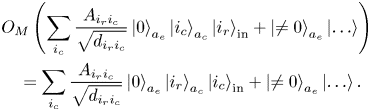
Finally, the oracles $O^{\dagger} _F O^{B}_{F,{\rm corr}}$ entangle the states encoding the column indices in the input register with the zero state in the ancilla register:
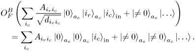
6.3 Single-target multicontrolled gates
If one has a single-target gate $G$ , whose matrix representation is
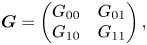
then the corresponding STMC gate $C_{\{q_{c\delta }\}}G^{(q_t)}$ is defined as the gate $G$
 acting on the target qubit $q_t$
 and controlled by a set of qubits $\{q_{c\delta }\}$
 . If $q_{c\delta }$
 is a control qubit then the gate $G$
 is triggered if and only if $\mid {\delta }\rangle_{q_{c\delta }}$
 , where $\delta = 0$
 or $1$
 . If the gate $G$
 acting on a quantum state vector ${\boldsymbol{\psi} }$
 of $n$
 qubits is controlled by the qubit $q_{c\delta } \in [0,n)$
 , then only the state vector's elements with the indices $\{i_e\}_{q_{c\delta }}$
 can be modified by the gate $G$
 :
:




For instance, for $q_{c1} = 0$ , every second element of ${\boldsymbol{\psi} }$
 can be modified by the gate $G$
 . Then, the STMC gate $C_{\{q_{c\delta }\}}G^{(q_t)}$
 can modify only the elements from the set
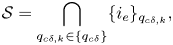
where $\bigcap$ is the intersection operator. The most common case is when $q_t$
 is a more significant qubit than the control ones, and the initial state of $q_t$
 is the zero state. In this case, the action of $C_{\{q_{c\delta }\}}G^{(q_t)}$
 can be described as

where $\eta _{k}$ are the complex amplitudes of the initial state of the control register.
6.4 General algorithm for the BE
To construct the BE oracle $U_A$ , we use the following general procedure.
(i) Introduce ancilla qubits necessary for intermediate computations in the oracle $U_A$
(§ 6.5).(ii) Assume that the bitstring of the qubits of the input register (also called the state register) encodes a row index of the matrix $\boldsymbol {A}$
.(iii) Using STMC gates, construct the oracle $U_D$
following the idea presented in (6.10) to encode column indices as a superposition of bitstrings in the state register (§ 6.6).(iv) Compute the matrix $\boldsymbol {D}^A$
or derive it using several matrices $\boldsymbol {D}^A$ constructed for matrices $\boldsymbol {A}$ of small sizes (§ 7.3).(v) Normalize the matrix $\boldsymbol {A}$
according to (6.7) using the non-sparsity-related parameter (6.14).(vi) Using STMC rotation gates, construct the oracle $O_H$
to perform the transformation (6.11) (§ 7).


Once the circuit for the oracle $U_A$ is constructed using STMC gates, one can transpile the circuit into a chosen universal set of elementary gates. Standard decomposition methods require at least $\mathcal {O}(n)$
 of basic gates (see Barenco et al. Reference Barenco, Bennett, Cleve, DiVincenzo, Margolus, Shor, Sleator, Smolin and Weinfurter1995), where $n$
 is the number of controlling qubits in an STMC gate. Yet, it was recently shown (see Claudon et al. Reference Claudon, Zylberman, Feniou, Debbasch, Peruzzo and Piquemal2023) that it is possible to decompose an arbitrary STMC gate into a circuit with $\mathcal {O}(\log _2(n)^{\log _2(12)}\log _2(1/\epsilon _{\rm STMC}))$
 depth where $\epsilon _{\rm STMC}$
 is the allowed absolute error in the approximation of the STMC gate. In our assessment of the BE oracle's scaling below, we assume that the corresponding circuit comprises STMC gates not decomposed into elementary gates.
6.5 Ancilla qubits for the BE
The first step to construct a circuit of the BE oracle is to introduce ancilla qubits and assign the meaning to their bitstrings. As seen from figure 1, the matrix $\boldsymbol {A}$ is divided into four submatrices. To address each submatrix, we introduce the ancilla qubit $a_f$
 . In combination with the register $r_f$
 introduced in (4.2), the register $a_f$
 allows addressing each submatrix in the following way:
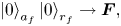
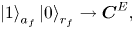
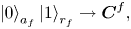
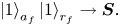
If $i_r$ and $i_c$
 are row and column indices of $\boldsymbol {A}$
 , respectively, such that


with integers $i_{fr}, i_{fc} = [0,1]$ , $i_{xr}, i_{xc} = [0, N_x)$
 and $i_{vr}, i_{vc} = [0, N_v)$
 , then the ancilla $a_f$
 encodes the integer $i_{fc}$
 .
.
According to figure 1, each submatrix is split into $N_x^2$ blocks of size $N_v\times N_v$
 each. Within each submatrix, only the diagonal and a few off-diagonal (in the submatrix $\boldsymbol {F}$
 ) blocks contain non-zero matrix elements. To address these blocks, we introduce the ancilla register $a_{xr}$
 with three qubits. This register stores the relative positions of blocks with respect to the main diagonal within each submatrix. The states $\mid {000}\rangle_{a_{xr}}$
 and $\mid {100}\rangle_{a_{xr}}$
 correspond to the blocks on the main diagonal of a submatrix. The states $\mid {001}\rangle_{a_{xr}}$
 and $\mid {010}\rangle_{a_{xr}}$
 correspond to the off-diagonal blocks shifted by one and two blocks to the right, respectively. The states $\mid {101}\rangle_{a_{xr}}$
 and $\mid {110}\rangle_{a_{xr}}$
 correspond to the off-diagonal blocks shifted by one and two blocks to the left, respectively. Using the same notation as in (6.24), the meaning of the register $a_{xr}$
 can be described schematically as follows:





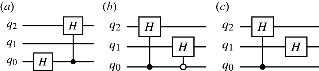
To encode the above bitstrings, one can use the circuits shown in figures 8(a) and 8(b).
(a) The circuit encoding the superposition of states $\mid {000}\rangle_q$ , $\mid {001}\rangle_q$
 and $\mid {101}\rangle_q$
 for a given input zero state. (b) The circuit encoding the superposition of states $\mid {000}\rangle_q$
 , $\mid {001}\rangle_q$
 and $\mid {010}\rangle_q$
 for a given input state produced by the circuit 8(a). To encode the superposition of states $\mid {100}\rangle_q$
 , $\mid {101}\rangle_q$
 and $\mid {110}\rangle_q$
 , one uses the same circuit except that an additional $X$
 gate is applied to the qubit $q_2$
 in the end. (c) The circuit encoding the superposition of states $\mid {000}\rangle_q$
 , $\mid {001}\rangle_q$
 , $\mid {010}\rangle_q$
 and $\mid {011}\rangle_q$
 for a given input state produced by the circuit 8(a). To encode the superposition of states $\mid {100}\rangle_q$
 , $\mid {101}\rangle_q$
 , $\mid {110}\rangle_q$
 and $\mid {111}\rangle_q$
 , one uses the same circuit except that an additional $X$
 gate is applied to the qubit $q_2$
 in the end.
In the submatrix $\boldsymbol {C}^f$ , some of the blocks have rows that contain $N_v$
 non-zero elements. To address these elements, we introduce the ancilla register $a_v$
 with $n_v$
 qubits. This register stores the integer $i_{vc}$
 (6.24) when the elements of $\boldsymbol {C}^f$
 and $\boldsymbol {C}^E$
 are addressed; otherwise, the register is not used. For instance, to address the non-zero elements in the submatrix $\boldsymbol {C}^f$
 , one uses the following encoding:

As regards to $\boldsymbol {C}^E$ , since all its non-zero elements have $i_{vc} = 0$
 , one keeps the register $a_v$
 in the zero state when $\mid {1}\rangle_{a_f}\mid {0}\rangle_{r_f}$
 .
.
The ancilla register $a_{vr}$ with three qubits is introduced to encode positions of the matrix elements within the non-zero blocks of the submatrix $\boldsymbol {F}$
 . In particular, the states $\mid {000}\rangle_{a_{vr}}$
 and $\mid {100}\rangle_{a_{vr}}$
 correspond to the elements on the main diagonal of a block. The states $\mid {001}\rangle_{a_{vr}}$
 , $\mid {010}\rangle_{a_{vr}}$
 and $\mid {011}\rangle_{a_{vr}}$
 correspond to the elements shifted by one, two and three cells, respectively, to the right from the diagonal. The states $\mid {101}\rangle_{a_{vr}}$
 , $\mid {110}\rangle_{a_{vr}}$
 and $\mid {111}\rangle_{a_{vr}}$
 correspond to the elements shifted by one, two and three cells, respectively, to the left from the diagonal. Using the notations from (6.24), the meaning of the register $a_{vr}$
 can be described as







To encode the above bitstrings, one can use the circuits shown in figures 8(b) and 8(c).
Also, we introduce the ancilla $a_e$ whose zero-state's amplitude will encode the complex value of a given matrix element.
6.6 Constructing the oracle ${U_D}$

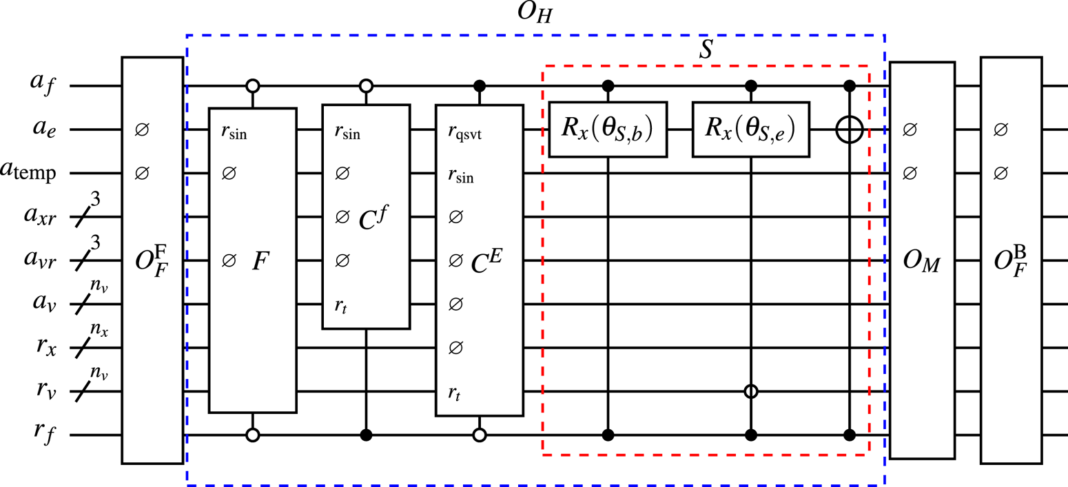
A schematic of the BE oracle $U_A$ is shown in figure 9, where the dashed blue box is the oracle $O_H$
 described in § 7, and the rest of the boxes are components of the oracle $U_D$
 .
.
The circuit representation of the BE oracle $U_A$ . The oracle $O_M$
 is shown in figure 11. The oracles $F$
 , $C^f$
 , $C^E$
 and $S$
 encode the corresponding submatrices introduced in (4.5), and are described in § 7. Here, the symbol $\varnothing$
 means that the gate does not use the corresponding qubit. The qubit $r_{\rm sin}$
 shown in some oracles indicates that the corresponding oracle includes the circuit shown in figure 15. The qubit $r_{\rm qsvt}$
 indicates that the oracle $C^E$
 is constructed using QSVT. The positions of the qubits $r_f$
 and $a_f$
 are changed for the sake of clarity.
The oracle $U_D$ is built ad hoc manually by considering its suboracles separately. The suboracle $O_F^{F} = O^{F}_{F,{\rm corr}} O_F$
 is constructed based on (6.15), where the ‘in’ register includes the registers $r_v$
 , $r_x$
 and $r_f$
 described in § 4.1. The ancilla registers $a_v$
 , $a_{vr}$
 , $a_{xr}$
 and $a_f$
 described in § 6.5 represent the $a_c$
 register in (6.15). For instance, the part of the circuit $O_F$
 encoding the ancilla $a_f$
 (6.23) is shown in figure 10, where the first Hadamard gate creates the address to the submatrices $\boldsymbol {F}$
 and $\boldsymbol {C}^E$
 , and the Pauli $X$
 gate generates the address to the elements of the submatrix $\boldsymbol {S}$
 with $i_{vr} > 0$
 (using the notation from (6.24)). The last Hadamard gate produces the addresses to $\boldsymbol {C}_f$
 and $\boldsymbol {S}$
 at $i_{vr} = 0$
 .
.


The implementation of the suboracle $O_F^{B} = O^{\dagger} _F O^{B}_{F,{\rm corr}}$ is done based on (6.18). Its correcting part $O^{B}_{F,{\rm corr}}$
 is implemented ad hoc by varying positions and control nodes of STMC gates.
The suboracle $O_M$ that performs the mapping (6.17) uses the SWAP gates to exchange the states in the registers $a_f$
 and $a_v$
 with the states in the registers $r_f$
 and $r_v$
 , respectively, as shown in figure 11. To encode absolute column indices into the input registers using the states of the registers $a_{xr}$
 and $a_{vr}$
 , one should follow the rules (6.25) and (6.27) and apply the quantum adders and subtractors described in Appendix C. The important feature of the oracle $O_M$
 is that the number of arithmetic operators in it does not depend on $N_x$
 or $N_v$
 . Since the circuits of the arithmetic operators scale as $\mathcal {O}(n_x)$
 or $\mathcal {O}(n_v)$
 depending on the target register of the operator, the scaling of $O_M$
 is $\mathcal {O}(n_x + n_v)$
 . The full circuit of $U_D$
 can be found in Novikau (Reference Novikau2024b). The modelling of the circuit is done using the QuCF framework (see Novikau Reference Novikau2024c), which is based on the QuEST toolkit (see Jones et al. Reference Jones, Brown, Bush and Benjamin2019).
The circuit of the oracle $O_M$ . The adders $A1$
 –$A3$
–$A3$ and the subtractors $S1$
 –$S3$
–$S3$ are described in Appendix C.
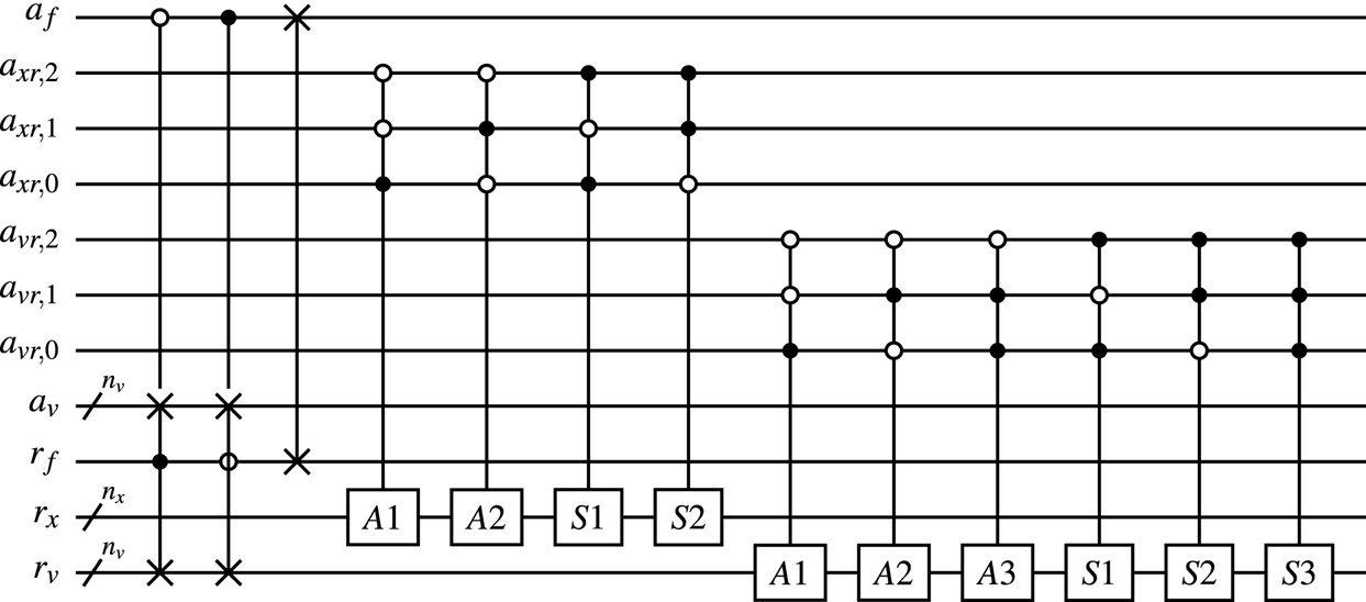
7 Construction of the oracle ${O_H}$

7.1 General strategy
The purpose of the oracle $O_H$ is to compute $A_{i_r i_c}$
 following (6.13). Therefore, further in the text, we consider the following rescaled matrix elements:
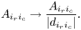
One can see from § 4.3 that two types of elements can be distinguished in $\boldsymbol {A}$ . The first type includes elements that depend only on the discretization and system parameters such as the antenna frequency $\omega _0$
 and the sizes of the grid cells. These elements sit in the submatrix $\boldsymbol {S}$
 (4.12) and the submatrix $\hat {\boldsymbol {F}}$
 introduced after (4.9). Since these elements appear mainly from the spatial, velocity and time derivatives, they remain mostly constant at bulk spatial and bulk velocity points, but become highly intermittent at spatial and velocity boundaries. The values of the elements of $\hat {\boldsymbol {F}}$
 strongly vary at boundaries of each $N_v\times N_v$
 block. Note that the submatrix $\hat {\boldsymbol {F}}$
 , which is a part of the matrix $\boldsymbol {A}$
 , is also subject to the rescaling (7.1). Thus, its elements change from one block to another depending not only on the original values of $\hat {\boldsymbol {F}}$
 (4.7), (4.8) and (4.9) but also on the specific implementation of $U_D$
 , which influences the rescaling (7.1).
Another type of element in $\boldsymbol {A}$ are those that depend on velocity $v$
 (and the background distribution function $H(v)$
 ). They form continuous profiles. However, this continuity can be lost after the rescaling (7.1). Such elements enter the submatrices $\boldsymbol {C}^f$
 , $\tilde {\boldsymbol {F}}$
 and $\boldsymbol {C}^E$
 , whose BE is described in §§ 7.5, 7.6 and 7.7, respectively.
7.2 The algorithm for BE $\hat {\boldsymbol {F}}$

7.2.1 Main idea
The main idea behind the algorithm for BE $\hat {\boldsymbol {F}}$ is to decompose this matrix into sets of elements such that all elements would have the same value within each set. After that, one extends large enough sets (as will be described further) in such a way that each extended set is encoded by a single STMC gate. However, after the extension, some sets may end up overlapping each other. In this case, the elements in the intersections (i.e. in the overlapping regions) should be corrected by additional STMC gates. The extension of some small sets that include a few matrix elements often leads to a significant overlapping with other sets. Therefore, it is often more efficient to encode a small set by encoding each element in it by its own STMC gate. Also, the representation of a matrix by sets is not unique. Because of that, we seek a minimal number of sets maximizing the number of large sets whilst minimizing the number of intersections and the number of small sets. Ideally, such optimization should be done using, for instance, deep reinforcement learning (see Sutton & Barto Reference Sutton and Barto2018). However, in the current version of the algorithm, the parameters are defined ad hoc.
This algorithm can be performed in $N_{\rm iter}$ iterations:

Here $O_H^{(1)}$ is the initial version of the oracle $O_H$
 , $O_H^{(k)}$
 is the correction to $O^{(1)}_H$
 provided by the $(k>1)$
 th iteration, and the final correction of the overlapping elements and encoding of small sets is performed at the $N_{\rm iter}$
 th iteration. After the $k$
 th iteration, one has

where the matrix $\boldsymbol {A}^{(k)}$ is encoded by the sequence $O_H^{(k)}\ldots O_H^{(2)} O_H^{(1)}$
 . If $\delta A^{(k)}_{i_r, i_c} = 0$
 then the first $k$
 iterations correctly encode the matrix element at the row $i_r$
 and the column $i_c$
 . If $|\delta A^{(k)}_{i_r, i_c}| > 0$
 then the corresponding element should be corrected. To do that, one considers the matrix
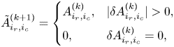
which provides information about which matrix elements still should be corrected. At the $(k+1)$ th iteration, one decomposes $\tilde {\boldsymbol {A}}^{(k+1)}$
 into sets whose extension is restricted by the condition that the extended sets would not overlap the zero elements of $\tilde {\boldsymbol {A}}^{(k+1)}$
 . The $(k+1)$
 th iteration constructs the oracle $O_H^{(k+1)}$
 correcting $\boldsymbol {A}^{(k)}$
 by using $\tilde {\boldsymbol {A}}^{(k+1)}$
 . The correcting procedure is discussed in § 7.2.4. Because each extension of sets may lead to additional overlapping elements, it is not guaranteed that the $(k+1)$
 iteration corrects all overlapping elements. For that reason, at the last iteration, the matrix $\tilde {\boldsymbol {A}}^{(N_{\rm iter})}$
 is encoded element by element without extending the sets. In other words, the $N_{\rm iter}$
 th iteration corrects all remaining badly encoded matrix elements without introducing its own errors, which otherwise appear during the sets extension. Finally, by varying the number $N_{\rm iter}$
 , one can construct the oracle $O_H$
 with a near-optimal scaling with respect to the matrix size.
7.2.2 Decomposition of the matrix
The elements in the submatrix $\hat {\boldsymbol {F}}$ are arranged along several diagonals (figure 1). The number of these diagonals is less or equal to the non-sparsity of the matrix $\boldsymbol {A}$
 and depends neither on $N_x$
 nor on $N_v$
 . Therefore, the first step is to represent $\hat {\boldsymbol {F}}$
 as a group $\{\mathcal {D}\}$
 of separate diagonals $\mathcal {D}$
 (figure 12a) and then consider each diagonal $\mathcal {D}$
 separately. One can specify a diagonal $\mathcal {D}$
 by using a constant integer $\Delta i$
 as
as

where ${\rm sign}_{\Delta i} = \Delta i / |\Delta i|$ . Each $\mathcal {D}$
 is encoded independently of other diagonals (as shown by various dashed blocks in figure 13) that results in a linear dependence of the depth of the oracle $O_H$
 on the non-sparsity $\varsigma _{\hat {\boldsymbol {F}}}$
 of the submatrix $\hat {\boldsymbol {F}}$
 .
.
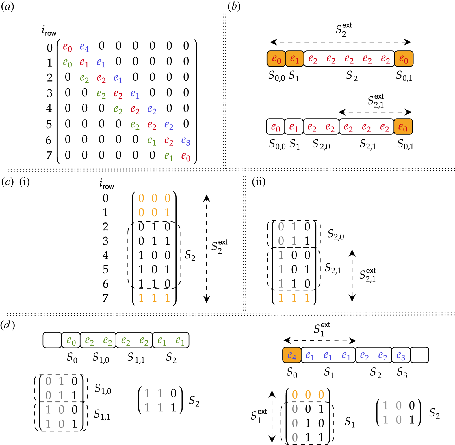
A schematic showing decomposition of a matrix into sets for the construction of the oracle $O_H$ . (a) A simple matrix of size $N_A = 8$
 is taken as an example. This matrix consists of three diagonals marked in different colours, and each diagonal is considered separately. The element values are indicated as $e_i$
 , where $e_i \neq e_j$
 if $i\neq j$
 . (b) A schematic showing how the main diagonal marked in red in (a) can be split in several sets where each set groups several matrix elements of the same value. (c-i) A matrix with bitstrings of the row indices of the original set $S_2$
 and of its extended version $S^{\rm ext}_{2}$
 . This extension results in three overlapping elements marked in orange, i.e. $S^{\rm ext}_2$
 overlaps elements of the sets $S_{0,0}$
 , $S_1$
 and $S_{0,1}$
 . (c-ii) A bitstring matrix of the set $S_2$
 that has been split into two sets, $S_{2,0}$
 and $S_{2,1}$
 , where only the latter is extended. This extension results in a single overlapping element. (d) A schematic showing the splitting and extension (if necessary) of sets in the left and right diagonals. The empty cells indicate that the considered diagonal does not have elements at the corresponding rows. The bits indicated in grey in the bitstring matrices are chosen as the control nodes of the STMC gates encoding the extended sets (figure 13).
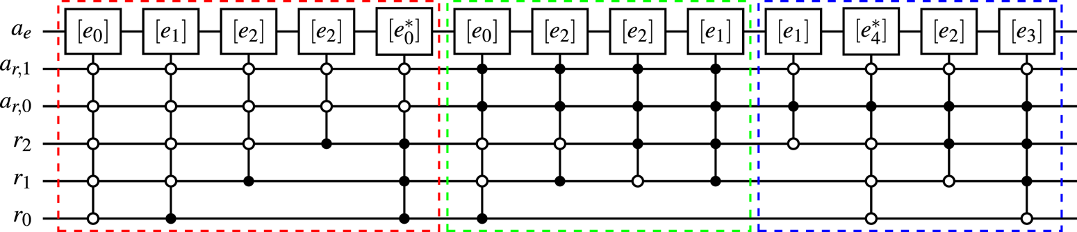
The circuit of the oracle $O_H$ encoding the elements of the tridiagonal matrix from figure 12(a). The dashed blocks indicate the parts of the oracle encoding the main diagonal (red box), the left diagonal (green box) and the right diagonal (blue box), correspondingly. Here, the register $r$
 encodes the matrix row indices. The ancilla register $a_r$
 has a similar meaning to that explained in (6.25) (although here the register has two qubits) and is used to address the matrix diagonals. The ancilla $a_e$
 is initialized in the zero state, and the matrix elements’ values are written into the amplitude of $\mid {0}\rangle_{a_e}$
 . The gate $[e_i]$
 is a schematic representation of a rotation gate whose rotation angle is chosen to encode the value $e_i$
 as explained in (6.13). The gate $[e_i^*]$
 is a rotation gate whose angle is computed taking into account the overlapping of the element $e_i$
 with one or several extended sets. For instance, the third gate in the red box encodes the set $S_{2,0}$
 . The fourth gate encodes the extended set $S_{2,1}^{\rm ext}$
 . Since $S^{\rm ext}_{2,1}$
 intersects with $S_{0,1}$
 , the angle for the fifth gate is computed taking into account the action of the fourth gate, as explained in § 7.2.4.
Each diagonal is represented by a group of sets $\{S\}$ where each set $S$
 contains elements of the same value $v^{(S)}$
 , i.e.

where $\{i_r\}$ are the row indices of all matrix elements described by the set $S$
 . Each set stores only $v^{(S)}$
 and $\{i_r\}$
 . A set can be divided into smaller sets (§ 7.2.5) and, thus, two different $S$
 can have the same $v^{(S)}$
 .
.
Once the matrix $\hat {\boldsymbol {F}}$ is split into $\{\mathcal {D}\}$
 , where $\mathcal {D} = \{S\}$
 , one constructs a circuit representation of $O_H$
 . The element-by-element encoding is inefficient, because it will require $\mathcal {O}(N_{xv})$
 quantum gates. The main purpose of our algorithm is to construct a circuit with the scaling better than $\mathcal {O}(N_{xv})$
 . Ideally, the scaling should be $\mathcal {O}(\text {polylog}(N_{xv})\varsigma _{\hat {\boldsymbol {F}}})$
 . (As shown in Novikau et al. (Reference Novikau, Dodin and Startsev2023), the QSVT for solving a multi-dimensional stationary wave problem described by a matrix of size $N$
 and non-sparsity $\varsigma$
 can have a polynomial speedup in comparison to classical conjugate-gradient-based algorithms if the corresponding BE oracle scales as $\mathcal {O}(\text {polylog}(N)\varsigma )$
 ).
).
To achieve a better scaling, the algorithm encodes the sets instead of the matrix elements by using the fact that each $S$ contains elements with the same value. The simplest way to encode $S$
 is to use a quantum arithmetic comparator (see Suau, Staffelbach & Calandra Reference Suau, Staffelbach and Calandra2021; Novikau et al. Reference Novikau, Dodin and Startsev2023) to find whether $i_r \in \{i_r\}_{S}$
 , where $i_r$
 is the row index encoded into the registers $r_v$
 , $r_x$
 and $r_f$
 (§ 4.1). However, for each $S$
 , one will need to use at least two comparators, and each comparator requires two ancilla qubits (although the ancillae can be potentially reused by various comparators). Instead, we try to arrange sets in such a manner that each large enough set would be encoded by a single STMC gate. Such an arrangement is performed by extending $S$
 . (Another possibility could be to use quantum arithmetic operators to encode the binary representation of the matrix elements. However, that would require much more qubits and be hard to test numerically, which is why we do not use this approach here.)
7.2.3 Set extension
To encode all elements of $S$ at once, the algorithm extends $S$
 in such a way that the extended set $S^{\rm ext}$
 is computed by a single STMC gate. To make it possible, it is necessary to complete $\{i_r\}$
 of $S$
 by another set $\{i_r^{\rm com}\}$
 such that the resulting set $\{i_r\}\cup \{i_r^{\rm com}\}$
 could be represented by (6.20) and (6.21). In other words, $S$
 is extended to ensure that it would be possible to find a STMC gate $C_{\{q_{c\delta }\}}G^{(a_e)}$
 such that $G_{00} = v^{(S)}$
 and $\mathcal {S} \equiv \{i_r\}\cup \{i_r^{\rm com}\}$
 .
.
The extended set $S^{\rm ext}$ consists of a core, which is the original non-extended set $S$
 , and a complement $S^{\rm com}$
 : $S^{\rm ext} = S \cup S^{\rm com}$
 and $S \cap S^{\rm com} = \varnothing$
 , where $S^{\rm com}$
 includes $N_c$
 elements described by the row indices $\{i_r^{\rm com}\}$
 :
:

Note here that the matrix elements $\hat {F}_{j, j + \Delta i}$ for $j \in \{i_r^{\rm com}\}$
 may have a value different from $v^{(S)}$
 but the extended set $S^{\rm ext}$
 assumes that they do have the value $v^{(S)}$
 . Thus, the extended sets can assign wrong values to some matrix elements. In this case, we speak about the overlapping of several sets. The cores of extended sets never intersect, $S_j \cap S_k = \varnothing$
 for $j\neq k$
 , but the complements can overlap with the cores or complements of other sets. Hence, one can have only complement–complement and complement–core overlapping. The matrix elements that sit in the overlapping regions of several sets should be corrected. The correction employs supplemental STMC gates. Therefore, it is important to minimize the number of overlapping elements. The correction can be done in different ways and a possible algorithm for that is described in § 7.2.4.
We should also note that, sometimes, small sets are extended to significantly larger sets, thus, drastically increasing the number of overlapping elements. Because of that, it is better to encode small enough sets such that each element in them is computed by a separate STMC gate.
In well-structured matrices, such as those that appear in classical linear wave problems, the number of sets is significantly less than the number of matrix elements. Since each extended set is encoded by a single STMC gate, the scaling of the resulting oracle should be significantly better than in the case when the matrix is encoded element by element. For instance, let us assume that a diagonal $\mathcal {D}$ consists of $N$
 elements. If all these elements are equal to each other then $\mathcal {D}$
 comprises a single set, and this set can be encoded into a quantum circuit by using a single STMC rotation gate. Another case is when there are $N_S$
 elements of the same value where $(N - N_S) \ll N$
 , then $\mathcal {D}$
 has a dominant set with $N_S$
 elements. This set can be extended to the whole diagonal as shown in figure 12(b) for the set $S_2$
 . In this case, the complement $S^{\rm com}$
 contains $(N-N_S) \ll N$
 elements and each of these elements are encoded by a separate STMC gate. This means that the oracle $O_H$
 encoding the diagonal $\mathcal {D}$
 has $(N-N_S + 1) \ll N$
 STMC gates.
However, extending the original set may not always be the best approach. Instead, $S$ can be split (§ 7.2.5) into several subsets and then each subset can be extended individually. As demonstrated in figure 12(b) for the set $S_2$
 , the splitting allows us to reduce the number of overlapping elements from $N_c = 3$
 to $N_c = 1$
 .
.
7.2.4 Correction of overlapping elements
If two sets intersect with each other, the overlapping elements should be corrected by supplemental gates. Let us consider the correction on the example from figure 12, where, for instance, two sets, $S_{2,1}^{\rm ext}$ and $S_{0,1}$
 , overlap at the element $e_0$
 . According to figure 12(c-ii), to encode the set $S_{2,1}^{\rm ext}$
 , one needs a single STMC gate controlled by the most significant qubit of the input register $r$
 (as shown in figure 13 by the fourth gate in the red box). To encode an arbitrary complex value, one can use the gate $R_c(2\theta _{z,2}, 2\theta _{y,2})$
 described in Appendix C, which should act at the zero state of the ancilla $a_e$
 . In particular, to compute the value $e_2$
 , one needs to chose the gates’ parameters in such a way that $e_2 = \cos (\theta _{y,2})\exp ({-\mathrm {i}\theta _{z,2}})$
 . In this case, one obtains

where $w_2$ is a complex value defined by the angles of the gate $R_c$
 . Thus, two components of the state $\psi _{\rm ext}$
 are $\psi _{\rm ext,0} = e_2$
 and $\psi _{\rm ext,1} = w_2$
 . This gate controlled by the most significant qubit of the register $r$
 (figure 13) entangles the state $\mid {\psi _{\rm ext}}\rangle_{a_e}$
 with the states $\mid {i_r}\rangle_{r}$
 , where $i_r = [4,7]$
 . However, at $i_r = 7$
 , the main diagonal has an element with the value $e_0$
 instead of $e_2$
 . This means that a supplemental gate $R_c(2\theta _{z,c}, 2\theta _{y,c})$
 should act on the state $\mid {\psi _{\rm ext}}\rangle_{a_e}\mid {7}\rangle_{r}$
 to encode the value $e_0$
 :
:

Here we are not interested in the value $w_0$ . This explains the last gate in the red box in figure 13, denoted $[e_0^*]$
 .
.
Equation (7.9) leads to the following equations for $\theta _{z,c}$ and $\theta _{y,c}$
 :
:


Here




In the more general case, when the $N_g$ gates act on the same element $e_{\rm res}$
 , then one can find $\theta _{y,c}$
 and $\theta _{z,c}$
 in (7.10)–(7.11) from


7.2.5 Set splitting
As we have already mentioned earlier, to minimize the number of overlapping elements, it may be more efficient to split sets such that the divided sets would have complements of smaller sizes and, thus, would require a smaller number of operations to correct the overlapping elements. Such splitting and reorganization of sets can be done in many different ways and, ideally, should be delegated to machine learning, which is likely to find a more optimal set organization than one can feasibly do manually ad hoc. However, there is also a simpler way to rearrange the sets, which is as follows. For each set, one constructs a matrix $\boldsymbol {A}_{\rm bits}$ with bitstrings representing the row indices of the set's elements as illustrated in figure 12(c,d). The size of $\boldsymbol {A}_{\rm bits}$
 is $N_S\times n_b$
 , where $N_S$
 is the set's size (the number of elements in the set) and $n_b = \log _2(N_A)$
 , where $N_A$
 is the size of the matrix to be described by $O_H$
 (in our case, the matrix is $\hat {\boldsymbol {F}}$
 and $N_A = N_{xv}$
 ).
).
The rows in $\boldsymbol {A}_{\rm bits}$ are enumerated by the index $r_b \in [0,N_S)$
 and store the bitstring representations of the rows of the matrix $\hat {\boldsymbol {F}}$
 . Each row $r_b$
 has $n_b$
 cells with bits of different significance, where the leftmost cell stores the most significant bit. Each column $c_b \in [0, n_b)$
 in $\boldsymbol {A}_{\rm bits}$
 contains an array of bits of equal significance (figure 12c). The column $c_b = 0$
 contains the most significant bits.
To decide how to split the set, one checks the leftmost $N_{\rm check}$ columns of $\boldsymbol {A}_{\rm bits}$
 . Let us assume that the leftmost column, $c_b = 0$
 , has the bit $\delta$
 at $r_b = 0$
 . If all bitcells at $c_b = 0$
 contain the same bit $\delta$
 , then one checks the bits in the next column. If $N_{\rm check}$
 columns have bitcells with unchanging bits, then the set remains undivided.
However, if the column $c_b < N_{\rm check}$ has a bit $\delta$
 at $r_b = 0$
 , but this bit changes at $r_{b,1}$
 , then one splits $\boldsymbol {A}_{\rm bits}$
 into two matrices, $\boldsymbol {A}_{\rm bits, 0}$
 and $\boldsymbol {A}_{\rm bits, 1}$
 . The former matrix is the part of $\boldsymbol {A}_{\rm bits}$
 with the rows $[0, r_{b,1})$
 , the latter matrix is the part of $\boldsymbol {A}_{\rm bits}$
 with the row $[r_{b,1}, N_S)$
 . These new matrices of bitstrings represent new sets. These sets still describe matrix elements with the same value, but now these elements are combined into two sets instead of the original single set. In this manner, $S_2$
 in the main diagonal in figure 12 is split into two sets, $S_{2,0}$
 and $S_{2,1}$
 .
.
One can vary $N_{\rm check}$ to find an optimal number of sets in $\mathcal {D}$
 , but usually it is better to keep this number significantly smaller than $n_b$
 because, otherwise, one can end up with a large number of small sets. This happens because the bits of low significance have a higher possibility to change within a set.
7.3 Extrapolation of the matrix ${D}^A$

To construct the oracle $O_H$ , one needs to compute the matrix $\boldsymbol {D}^A$
 related to the oracle $U_D$
 (6.9) to perform the rescaling (6.13). The parts of $\boldsymbol {D}^A$
 related to the submatrices $\boldsymbol {C}^E$
 , $\boldsymbol {C}^f$
 and $\boldsymbol {S}$
 have a trivial structure and can be predicted for any $N_x$
 and $N_v$
 . For instance, $D^A_{N_{xv} + i_x N_v + i_v,\ N_{xv}+ i_x N_v + i_v} = 1$
 for $i_x = [0, N_x)$
 and $i_v = [1, N_v)$
 . These elements correspond to the main diagonal of the submatrix $\boldsymbol {S}$
 , where the matrix non-sparsity is $1$
 . In the rows with indices $N_{xv} + i_x N_v$
 , the column indices of the non-zero elements are computed by a single Hadamard gate acting on the ancilla $a_f$
 and by $n_v$
 Hadamard gates acting on all qubits of the register $a_v$
 . (These Hadamard gates appear in both $O_F$
 and $O_F^{\dagger}$
 , according to (6.9) and figure 10.) Because of that, $D^A_{N_{xv} + i_x N_v,\ N_{xv}+ i_x N_v} = 1/2$
 that corresponds to the diagonal elements at $i_v = 0$
 in the submatrix $\boldsymbol {S}$
 , and $D^A_{N_{xv} + i_x N_v,\ i_x N_v + i_v} = 1/2^{n_v/2+1}$
 with $i_v = [0, N_v)$
 that corresponds to the non-zero elements of the submatrix $\boldsymbol {C}^f$
 .
.
Let us denote the upper left $N_{xv}\times N_{xv}$ part of $\boldsymbol {D}^A$
 as $\boldsymbol {D}^F$
 . The submatrix $\boldsymbol {D}^F$
 contains elements $d_{i_r i_c}$
 by which the submatrix $\boldsymbol {F}$
 should be rescaled in (6.13). The computation of $\boldsymbol {D}^F$
 is numerically challenging for a large $N_{xv}$
 . Instead, $\boldsymbol {D}^F$
 of a large size can be extrapolated by using known matrices $\boldsymbol {D}^F$
 of several small sizes. To do that, one creates a template of $\boldsymbol {D}^F$
 by using computed $\boldsymbol {D}^F$
 for small $N_x$
 and $N_v$
 . This can be done because the relative positions of the submatrix elements and the elements’ values do not change with the increase of $N_{xv}$
 . The template is used to reconstruct $\boldsymbol {D}^F$
 for any $N_{xv}$
 . The algorithm for the creation of this template is the following.
Let us consider the matrix $\boldsymbol {D}^F$ that is split into several diagonals in the same way as described in § 7.2.2. The algorithm considers each of these diagonals independently and assumes that the row index $r$
 of this matrix depends on $N_{\rm ind}$
 indices $r_l$
 :
:
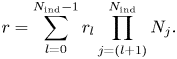
Here each index $r_l = [0, N_l)$ corresponds to the $l$
 th dimension of the size $N_l$
 and $N_{N_{\rm ind}} = 1$
 . For instance, any matrix describing dynamics in three-dimensional real space ($N_{\rm ind} = 3$
 ) has $r = r_0 N_y N_x + r_1 N_x + r_2$
 . In our case, $r_0 = i_{xr}$
 and $r_1 = i_{vr}$
 according to (6.24). Also, we define the following ordered set of indices:

The ordered set $\overrightarrow {\{r\}}_{l}$ is empty if $l = 0$
 .
.
Let us consider the diagonal $\mathcal {D}$ defined in (7.5), where instead of $\hat {\boldsymbol {F}}$
 we now take $\boldsymbol {D}^F$
 . The vector with all matrix elements from $\mathcal {D}$
 is denoted $\boldsymbol {M}$
 . It has $N_{xv}$
 elements, where we formally define $M_{r} = \varnothing$
 if the diagonal does not have any element at the row $r$
 . Due to the dependence (7.13), $\boldsymbol {M}$
 has a nested structure with $N_0$
 blocks, where each block has $\prod _{j=1}^{N_{\rm ind}} N_j$
 rows. These rows can be combined into $N_1$
 sub-blocks, where each sub-block has $\prod _{j=2}^{N_{\rm ind}} N_j$
 rows, and so on. Let us call all blocks of an equal size a layer. There are $N_{\rm ind}$
 layers. The $i_l$
 th block in the $l$
 th layer is defined as

where $i_l = [0, N_l)$ , $l = [0, N_{\rm ind})$
 and each block of the $(N_{\rm ind} - 1)$
 th layer is a single matrix element, i.e.
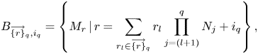
where $q = N_{\rm ind} - 1$ . Hence, the $l$
 th layer has $N_l$
 blocks, and each of these blocks has $\prod _{j=l+1}^{N_{\rm ind}} N_j$
 matrix elements.
Identical adjacent blocks in the $l$ th layer are combined into blocksets. A blockset in the $l$
 th layer is denoted $\mathcal {B}_l$
 and is defined as

where each blockset in the $q = (N_{\rm ind} - 1)$ th layer combines identical neighbour matrix elements

Since each block in the $l$ th layer includes blocks from the $(l+1)$
 th layer (7.15), each block can be described by a group of blocksets, i.e.

where we keep the index $i_l$ to indicate that $\{\mathcal {B}_{l+1}\}_{i_l}$
 represents the $i_l$
 th block at the $l$
 th layer. If the block $B_{\overrightarrow {\{r\}}_{-1},i_{-1}}$
 is formally defined as the whole diagonal $\boldsymbol {M}$
 , then $\{\mathcal {B}_{0}\}_{i_{-1}}$
 is a group of blocksets where the blocks of the zeroth layer are sorted. By combining (7.17) and (7.19), one can see that each blockset in the $l$
 th layer can be defined as a group of blocksets from the $(l+1)$
 th layer:

Thus, the whole diagonal $\boldsymbol {M}$ can be represented as nested blocksets. Representing a matrix by a group of diagonals comprising blocksets can be regarded as creating a template that represents a compressed image of the matrix.
In the matrix $\boldsymbol {D}^F$ , the number of diagonals $\mathcal {D}$
 does not change with $N_{xv}$
 . The matrix elements $M_r$
 stored in the blocksets (7.18) are also independent of $N_{xv}$
 . (Some matrix elements of $\boldsymbol {D}^A$
 do change with $N_v$
 because the non-sparsity of $\boldsymbol {C}^f$
 and $\boldsymbol {C}^E$
 changes with $N_v$
 . Yet, the non-sparsity of the submatrix $\boldsymbol {F}$
 does not change with $N_{xv}$
 , and because of that, the elements of $\boldsymbol {D}^F$
 do not change as well.) The indices $r_b$
 and $r_e$
 in (7.20) and (7.18) depend linearly on $N_l$
 , i.e.


where $l=[0,N_{\rm ind})$ . The unknown coefficients $\alpha _b$
 , $\alpha _e$
 , $\beta _b$
 and $\beta _e$
 are different for different blocksets. To compute these coefficients, one constructs the templates for $N_{\rm ind}+1$
 matrices where each matrix has at least one $N_l$
 different from the corresponding $N_l$
 of all other matrices. (If needed, each of the $N_{\rm ind}+1$
 matrices can have all $N_{\rm ind}$
 dimensions different from the dimensions of other matrices.) For each of these computed $(N_{\rm ind}+1)$
 templates, one knows the row indices $r_b$
 and $r_e$
 for each blockset. One substitutes these indices to (7.21) from which the unknown coefficients can now be calculated.
Once the coefficients are computed, one can construct $\boldsymbol {D}^F$ of an arbitrary size $N_{xv}$
 . Equations (7.21) allow us to compute the positions $r_b$
 and $r_e$
 for all blocksets in $\boldsymbol {D}^F$
 for the required $N_{xv}$
 .
.
For the matrix $\boldsymbol {D}^F$ , $N_{\rm ind}$
 equals two, where $N_0 = N_x$
 an $N_1 = N_v$
 . Thus, one needs to precalculate three matrices $\boldsymbol {D}^F$
 with various $N_x$
 and $N_v$
 to use (7.21). Yet, one should keep in mind that $N_x$
 and $N_v$
 should be large enough to take into account the influence of the boundary elements in $\boldsymbol {D}^F$
 properly. More precisely, one should consider only matrices with $n_x \geq 4$
 and $n_v \geq 4$
 .
.
As an example illustrating the decomposition of a matrix into blocksets, let us consider a diagonal matrix $\boldsymbol {D}^{\rm ex}$ with diagonal elements $D^{\rm ex}_{i, i}$
 , where $i = i_y N_x + i_x$
 with $i_y = [0,N_y)$
 and $i_x = [0,N_x)$
 for $N_y = 2^{n_y}$
 and $N_x = 2^{n_x}$
 :
:




Here, $e_0$ and $e_1$
 are some non-equal values. Due to the dependence on the indices $i_x$
 and $i_y$
 , the main diagonal has a nested structure with $N_y$
 blocks and with $N_x$
 elements in each block. Other diagonals are empty (the matrix elements in these diagonals are equal to zero). The main diagonal for different $n_y$
 and $n_x$
 is shown in figure 14.
A schematic showing elements in the main diagonal of the matrix $\boldsymbol {D}^{\rm ex}$ described in (7.22) for various $N_x = 2^{n_x}$
 and $N_y = 2^{n_y}$
 . The matrix has $N_y$
 blocks with $N_x$
 elements each. These blocks are grouped into two blocksets, $\mathcal {B}_0^I$
 and $\mathcal {B}_0^{II}$
 . The elements in each block of the blockset $\mathcal {B}_0^I$
 are combined into two blocksets indicated by different shades of green. The elements in each block of the blockset $\mathcal {B}_0^{II}$
 are combined into three blocksets indicated by different shades of blue.
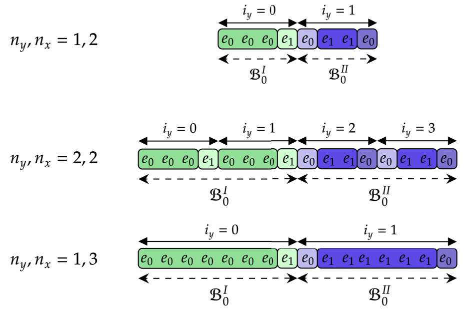
In the zeroth layer the diagonal is split into two blocksets, $\mathcal {B}_0^I$ and $\mathcal {B}_0^{II}$
 , independently of the matrix size. In the next layer, $\mathcal {B}_0^I$
 contains two blocksets (which are indicated by different shades of green in figure 14), and $\mathcal {B}_0^{II}$
 contains three blocksets (indicated by different shadows of blue). Although the number of blocks and elements in $\boldsymbol {D}^{\rm ex}$
 changes with $N_x$
 and $N_y$
 , the number of blocksets in any layer does not. For instance, independently of $N_y$
 , the blockset $\mathcal {B}_0^{I}$
 always contains only two blocksets. Indeed, according to (7.17), $\mathcal {B}_0^{I}$
 stores a single copy of one of $N_y/2$
 identical blocks in the first half of the diagonal. In turn, this single copy contains two blocksets, one of which saves a single copy of the elements $e_0$
 and another saves the element $e_1$
 .
.
The indices stored by the blockset $\mathcal {B}_0^{I}$ are
are

The indices of the first inner blockset of $\mathcal {B}_0^{I}$ are $r_b = 0$
 and $r_e = N_x-2$
 . The indices of the second inner blockset are $r_b = N_x-2$
 and $r_e = N_x-1$
 .
.
The blockset $\mathcal {B}_0^{II}$ have the following boundaries:

The indices of the inner blocksets of $\mathcal {B}_0^{II}$ can be easily found from figure 14 or (7.22).
7.4 Encoding the submatrix ${S}$

To encode the submatrix $\boldsymbol {S}$ described in (4.12), we use the two gates $R_x$
 with the following angles:


As one can see from the red dashed box in figure 9, the elements of $\boldsymbol {S}$ are encoded by three gates, $R_x(\theta _{S,b})$
 , $R_x(\theta _{S,e})$
 and $X$
 , applied to the ancilla $a_e$
 . The first gate $R_x(\theta _{S,b})$
 encodes $\mathrm {i}\omega _0$
 into the amplitude of the zero state of the ancilla $a_e$
 . Due to the rescaling (7.1), the value $\mathrm {i}\omega _0$
 of each element at $i_{vr} = 0$
 in $\boldsymbol {S}$
 is multiplied by the factor $2$
 . This is taken into account by the second gate, $R_x(\theta _{S,e})$
 , which corrects the action of $R_x(\theta _{S,b})$
 .
.
7.5 Encoding the submatrix ${C}^f$

To encode the matrix elements of $\boldsymbol {C}^f$ (4.11) that depend on the velocity, we use the circuit shown in figure 15. It encodes the function $\sin (\phi _i)$
 for $i = [0, N_t)$
 with $N_t = 2^{n_t}$
 :
:

Here $n_t$ is the number of qubits in the register $r_t$
 and $\Delta \phi = 2\alpha _1/N_t$
 . This circuit scales as $\mathcal {O}(n_t)$
 .
.
The circuit encoding $\sin (\phi _i)$ according to (7.26). Here, $R_k = R_y(2\alpha _1/2^k)$
 .
.
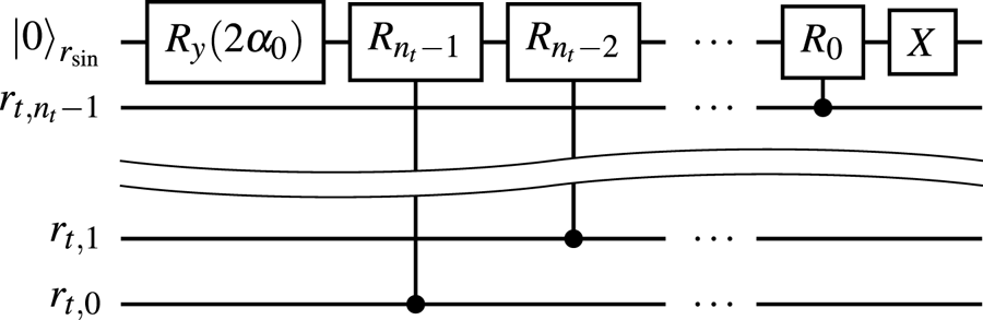
To encode the velocity grid $v_i$ , where $v_{\rm max}\ll 1$
 due to the normalization (6.7), one can use the circuit 15, since $\sin (\phi _i) = \phi _i + \mathcal {O}(\phi _i^3)$
 . In this case, $n_t = n_v$
 , $\alpha _0 = - v_{\rm max}$
 and $\alpha _1 = |\alpha _0| N_v/ (N_v - 1)$
 . All non-zero elements of the submatrix $\boldsymbol {C}^f$
 are encoded by using a single call to the circuit 15.
7.6 Encoding the submatrix $\tilde {{F}}$

The elements of $\tilde {\boldsymbol {F}}$ described after (4.9) depend on $v$
 linearly and are encoded using the same technique described in § 7.5.
7.7 Encoding the submatrix ${C}^E$

To encode the matrix elements of $\boldsymbol {C}^E$ (4.10), one can use the QSVT to approximate the odd function $v H(v)$
 . First of all, the odd function $v H(v)$
 is approximated by the form

where $y_i = \sin (\phi _i)$ for $i = [0, N_v)$
 where the angles $\phi _i$
 are computed using (7.26) with the parameters $\alpha _0 = -1$
 and $\alpha _1 = |\alpha _0| N_v/(N_v-1)$
 . The parameter $p_0$
 depends neither on $n_x$
 nor on $n_v$
 . The parameter $p_1$
 decreases linearly with $N_v$
 and does not depend on $N_x$
 . The approximation $f_{vH}(y_i) = v_i H(v_i) \pm \varepsilon _{\rm ce, appr}$
 is found by solving a nonlinear least-square problem.
The function $f_{vH}(y_i)$ is computed by using QSVT, where the variable $y_i$
 is encoded by the circuit 15. Because flat background temperature and density profiles are considered, this function does not depend on $x$
 and can be encoded for all $x$
 points by a single call to the QSVT circuit. The absolute error $\epsilon _{\rm CE, qsvt}$
 of the QSVT computation of the function (7.27) rapidly decreases with the number of QSVT angles $N_{\rm CE,qsvt}$
 , e.g. $\epsilon _{\rm CE, qsvt} = 10^{-6}$
 for $N_{\rm CE,qsvt} = 16$
 . Each QSVT angle is associated with a single call to the oracle 15 that scales linearly with $n_v$
 . Thus, the scaling of the circuit encoding the submatrix $\boldsymbol {C}^E$
 is $\mathcal {O}(n_v \log _2(\epsilon _{\rm CE, qsvt}^{-1}))$
 .
.
If the temperature and density depend on the spatial coordinate, then one needs to implement additional QSVT circuits that would encode the change in the amplitude and the width of the bumps of the function $v H$ . Another option is to substitute these QSVT circuits by a single one by applying multivariable QSP (see Rossi & Chuang Reference Rossi and Chuang2022) that operates with several BE oracles at once, thus computing a polynomial of multiple variables, i.e. $x$
 and $v$
 in our case.
7.8 Scaling of the BE oracle
The final circuit of the BE oracle encoding the matrix $\boldsymbol {A}$ can be found in Novikau (Reference Novikau2024b) and was numerically tested using the QuCF framework (Novikau Reference Novikau2024c). Now, let us estimate the scaling of this circuit. It comprises the scaling of the oracle $U_D$
 and the oracle $O_H$
 . As discussed in § 6.6, $U_D$
 scales as $\mathcal {O}(n_x + n_v)$
 due to the arithmetic operators. The circuit of $O_H$
 consists of several pieces: the oracle encoding the submatrix $\hat {\boldsymbol {F}}$
 , whose encoding is performed by the procedure discussed in § 7.2, and the oracles encoding the submatrices $\boldsymbol {S}$
 (§ 7.4), $\boldsymbol {C}^f$
 (§ 7.5), $\tilde {\boldsymbol {F}}$
 (§ 7.6) and $\boldsymbol {C}^E$
 (§ 7.7). The scaling of the circuit for $\hat {\boldsymbol {F}}$
 is shown in figure 16 and is estimated as $\mathcal {O}(\varsigma _{\hat {\boldsymbol {F}}}{\rm poly}(N_x) {\rm poly}(n_v))$
 . The poor scaling with respect to $N_x$
 is caused by the matrix elements that appear due to the non-zero diffusivity $\eta$
 (2.11). The non-sparsity $\varsigma _{\hat {\boldsymbol {F}}}$
 of the submatrix $\hat {\boldsymbol {F}}$
 does not change with $N_x$
 or $N_v$
 . Yet, $\varsigma _{\hat {\boldsymbol {F}}}$
 depends on the discretization method or boundary conditions of the simulated kinetic model.
The dependence of the number of non-zero elements $N_{\rm nz}$ in the matrix $\boldsymbol {F}_F$
 on (a) $n_v$
 for various $n_x$
 and on (b) $n_x$
 for various $n_v$
 . (c) The dependence of the number of STMC gates in the oracle $O_H$
 necessary for encoding $\boldsymbol {F}_F$
 on $n_v$
 for various $n_x$
 . (d) The dependence of the number of STMC gates on $n_x$
 for various $n_v$
 . Here, the text in different colours indicate the fitting equations approximating the scaling with respect to $n_v$
 and $n_x$
 or $N_v$
 and $N_x$
 .
.
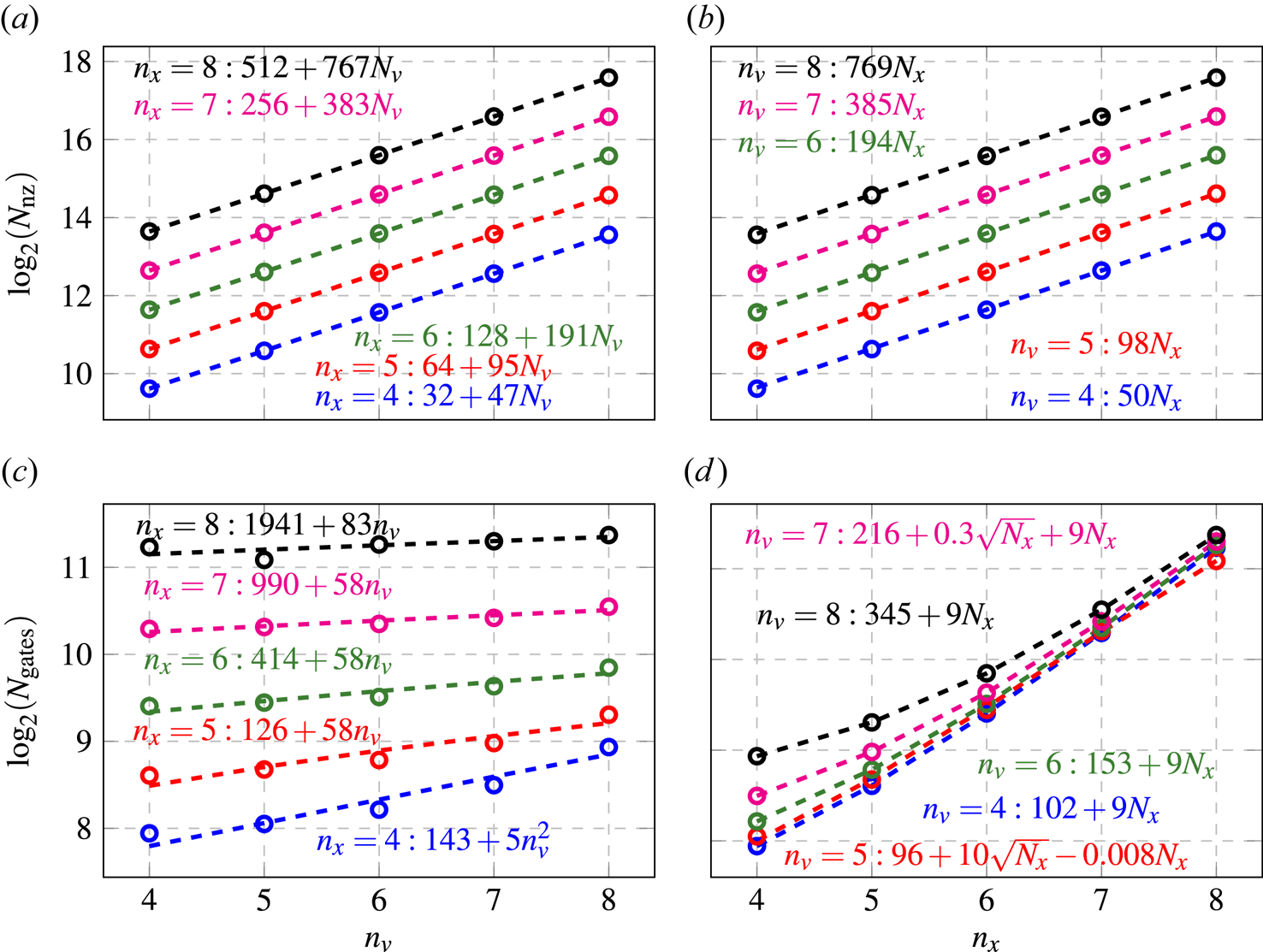
The depth of the circuit for $\boldsymbol {S}$ scales as $\mathcal {O}(1)$
 if one uses STMC gates, and, according to Claudon et al. (Reference Claudon, Zylberman, Feniou, Debbasch, Peruzzo and Piquemal2023), an arbitrary STMC gate controlled by $n$
 qubits can be decomposed into a circuit with $\mathcal {O}(\log _2(n)^{\log _2(12)}\log _2(1/\epsilon _{\rm STMC}))$
 depth, as mentioned in § 6.4. The oracles for $\boldsymbol {C}^f$
 and $\tilde {\boldsymbol {F}}$
 scale as $\mathcal {O}(n_v)$
 . The scaling of the oracle $\boldsymbol {C}^E$
 implemented using QSVT is $\mathcal {O}(n_v\log _2(\epsilon _{\rm CE, qsvt}^{-1}))$
 .
.
Then, in summary, the main contribution to the scaling of the BE oracle of the whole matrix $\boldsymbol {A}$ is due to the oracle encoding $\hat {\boldsymbol {F}}$
 , and the resulting scaling is

8 Discussion
A complete QSVT circuit for modelling a boundary-value problem was tested in Novikau et al. (Reference Novikau, Dodin and Startsev2023). The QSVT circuit discussed here has a similar structure up to the BE oracle, so, in principle, it can be done similarly. However, this is currently beyond the capabilities of the QuCF framework, as the kinetic problem considered here requires significant computational resources. Specifically, the BE oracle alone involves $2n_v + n_x + 11$ qubits, and our test (§ 5) requires at least $n_v = 5$
 and $n_x = 7$
 . Hence, the total number of qubits in the BE oracle must be $28$
 or more. Apart from this, the QSVT circuit needs an extra ancilla, and the initialization block needs at least two extra ancillae. Thus, the minimum number of qubits of the entire circuit for the matrix inversion is $31$
 . Moreover, the inversion of the considered matrix, which has the condition number around $10^5$
 , requires millions of calls of the BE oracle. Extraction of classical information further increases the circuit complexity. As usual, extracting all the information would require a large number of measurements and, therefore, is not an option, as that would rule out quantum speedup. To retain the speedup, one can measure just a few integral characteristics, such as the electric-field energy. This can be done using amplitude-estimation-based techniques discussed by Novikau et al. (Reference Novikau, Dodin and Startsev2023). Note, though, that, even then, the amplitude estimation (Brassard et al. Reference Brassard, Høyer, Mosca and Tapp2002) requires at least $\mathcal {O}(\kappa _{A})$
 repetitions of the QSVT circuit, which makes it necessary to use preconditioning.
8.1 Preconditioning
As mentioned earlier, a QSVT-based algorithm for solving (1.1) essentially amounts to inverting the matrix $\boldsymbol {A}$ . Unfortunately, for boundary-value wave problems, and kinetic problems in particular, $\boldsymbol {A}$
 typically has a large condition number $\kappa _{A}$
 . This makes accurate inversion challenging and also complicates extracting classical information, since the success probability of the circuit scales as $O(\kappa _A^{-1})$
 (see Novikau et al. Reference Novikau, Dodin and Startsev2023). A solution to this can be to find a good preconditioner. Specifically, suppose one finds a matrix $\boldsymbol {P}$
 such that the matrix $\boldsymbol {P}\boldsymbol {A}$
 has a much smaller condition number than that of $\boldsymbol {A}$
 , $\kappa _{PA} \ll \kappa _{A}$
 . From (1.1), it follows that

Then, the matrix $\boldsymbol {P}\boldsymbol {A}$ is easier to invert than the original matrix $\boldsymbol {A}$
 , so it may be possible to easily calculate the solution in the form

A schematic of the QSVT circuit with a preconditioner is shown in figure 17. Here, $\boldsymbol {P}$ is computed by the separate BE oracle $U_P$
 , the oracles $U_A$
 and $U_b$
 can be the same as in the problem without a preconditioner, so the only additional step needed is to implement $U_P$
 . An advantage of this approach (compared with constructing oracles for $\boldsymbol {P}\boldsymbol {A}$
 and $\boldsymbol {P}\boldsymbol {b}$
 ) is that $U_P$
 does not have to be constructed precisely. If, instead of the intended $\boldsymbol {P}$
 , $U_P$
 encodes a slightly different preconditioner $\boldsymbol {P}'$
 , this changes (8.1) into $\boldsymbol {P}'\boldsymbol {A} \psi = \boldsymbol {P}'\boldsymbol {b}$
 , but the latter is still equivalent to the original (1.1) leading to an equivalent solution $\psi = (\boldsymbol {P}'\boldsymbol {A})^{-1}\boldsymbol {P}'\boldsymbol {b}$
 . As long as the condition number of $\boldsymbol {P}'\boldsymbol {A}$
 is comparable to that of $\boldsymbol {P}\boldsymbol {A}$
 , the matrix $\boldsymbol {P}'$
 serves the role of a preconditioner just as well as the matrix $\boldsymbol {P}$
 and, thus, the modified $U_{P}$
 is just as good as the intended $U_P$
 .
.
A schematic of the circuit that solves the preconditioned system (8.1). The oracle $U_P$ encodes the preconditioner $\boldsymbol {P}$
 , the oracle $U_A$
 encodes the original matrix $\boldsymbol {A}$
 . The oracle $U_b$
 encodes the right-hand-side vector $\boldsymbol {b}$
 into the input register ‘in’ that is originally initialized in the zero state. The blue box highlights the QSVT circuit that encodes an odd polynomial approximating the inverse matrix $(\boldsymbol {P}\boldsymbol {A})^{-1}/\kappa _{PA}$
 . The gates denoted as $\phi _{k}$
 correspond to the controlled rotations indicated by the grey dashed boxes in figure 7.

The implementation of the combined operator $U_P U_A$ may require a simple compression gadget (see Fang, Lin & Tong Reference Fang, Lin and Tong2023) to guarantee correct computation of the product $\boldsymbol {P}'\boldsymbol {A}$
 . This gadget will need two ancillae, two quantum decrementors and the adder $A2$
 (figure 19), i.e. the arithmetic operators that scale linearly with the number of qubits in the gadget. Thus, the gadget will not deteriorate the overall algorithm scaling.
8.2 Remaining challenges
The main issues that remain to be addressed in future works are the following. The spectral norm of our BE is around $10^{-2}$ . This significantly worsens the QSVT scaling. The main reason for this is that, in our current version of the BE, the oracle $U_D$
 is not optimized. To bring the norm close to one, an optimization procedure for constructing a more optimal version of the oracle $U_D$
 is needed. The algorithm can be based on the same foundations discussed in § 7.
Another issue, which has already been mentioned in § 6.1, is that the encoding of the source with a non-trivial profile may significantly reduce the success probability of the overall quantum algorithm. For instance, both QSVT or QETU methods compute a Gaussian with success probability scaling as $\mathcal {O}(\sigma _G/x_{\rm max})$ , where $\sigma _G$
 is the width of the Gaussian (see Kane et al. Reference Kane, Gomes and Kreshchuk2023). To increase the probability, it may be better to approximate the source profile with a different function that is easier to encode. For instance, the encoding of a strongly localized source (i.e. $\delta$
 function) requires one or several Pauli $X$
 gates and has the success probability equal to unity. An impulse with the amplitude $2^{-n_s/2}$
 potentially can be encoded using $n_s$
 Hadamard gates and $\mathcal {O}(n_s)$
 Pauli $X$
 gates. Hence, it may be possible to approximate a given source by a set of pulses, which then can be encoded efficiently and ensure a high success probability at the same time.
9 Conclusions
In this paper we propose an algorithm for encoding linear kinetic plasma problems in quantum circuits. The focus is on modelling electrostatic linear waves in a one-dimensional Maxwellian electron plasma. The waves are described by the linearized Vlasov–Ampère system with a spatially localized external current that drives plasma oscillations. This system is formulated as a boundary-value problem and cast in the form of a linear vector equation (1.1) that can be solved using the QSP-based algorithm. The latter requires encoding of the matrix $\boldsymbol {A}$ in a quantum circuit as a sub-block of a unitary matrix. We developed an algorithm for BE $\boldsymbol {A}$
 into a circuit using a compressed form of the matrix. This significantly improves the scaling of the resulting BE oracle with respect to the velocity coordinate. However, further analysis is required to improve the scaling along the spatial coordinate. The proposed algorithm can serve as a foundation for developing BE algorithms in more complex kinetic linear plasma problems, for example, for modelling of electromagnetic waves in magnetized plasma.
Acknowledgements
The authors thank Ilon Joseph for valuable discussions.
Editor Nuno Loureiro thanks the referees for their advice in evaluating this article.
Funding
The research described in this paper was supported by the Laboratory Directed Research and Development (LDRD) Program at Princeton Plasma Physics Laboratory (PPPL), a national laboratory operated by Princeton University, and by the U.S. Department of Energy (DOE) Office of Fusion Energy Sciences ‘Quantum Leap for Fusion Energy Sciences’ Project No. FWP-SCW1680 at Lawrence Livermore National Laboratory (LLNL). Work was performed under the auspices of the U.S. DOE under PPPL Contract DE-AC02-09CH11466 and LLNL Contract DE-AC52–07NA27344.
Declaration of interests
The authors report no conflict of interest.
Data availability statement
The open-source freely available C++ code of the QuCF framework used for the emulation of the quantum circuits created in this work can be found in Novikau (Reference Novikau2024c). The detailed structure of the quantum circuits can be found in Novikau (Reference Novikau2024b).
Appendix A. Analytical solution
Here, we derive an analytical solution of (2.4) for the special case when the plasma is homogeneous ($n = T = 1$ ). By applying the Laplace transform (Appendix B) to (2.4), we obtain

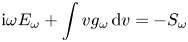
(assuming $g_0 \equiv g(t=0) = 0$ ), where $S_\omega = E_0 - j^{(S)}_\omega$
 due to (B2). Let us also apply the Fourier transform in space (Appendix B), assuming zero boundary conditions at infinity (i.e. ${g}_\omega |_{x\to \pm \infty } = E_\omega |_{x\to \pm \infty } = 0$
 ). This leads to


From the above equations, we obtain
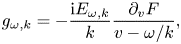

For the background Maxwellian distribution (2.6), the electric field becomes
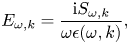

where $\xi = \omega /(k\sqrt {2})$ , and the function $Z_0(\xi )$
 is defined via the plasma dispersion function $Z(\xi ) = \sqrt {{\rm \pi} }\,{\rm e}^{-\xi ^2}[\mathrm {i} - {\rm erfi}(\xi )]$
 as (see Stix Reference Stix1992)
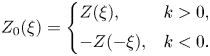
By applying the Laplace transform in time and the Fourier transform in space to (2.2), we also obtain

where $\rho ^{(S)}_{0,k} = \rho ^{(S)}_k(t = 0)$ , whilst the initial electric field satisfies the Gauss’ law:
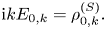
Thus, we obtain

from where one can see that
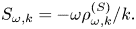
As a result, (A4a) yields
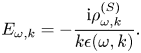
Let us assume an oscillating source charge density:

This corresponds to
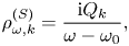
and (A10) yields
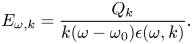
To find the evolution of the electric field in time, we perform the inverse Laplace transform (B4):

We are interested only in the established spatial distribution of the electric field that is observed at $t\to +\infty$ . Because of the Maxwellian background distribution (2.6), the plasma is stable, i.e. ${\rm Im}\,\omega _q(k)\leq 0$
 , for all $q \geq 1$
 . Therefore, $\exp ({-\mathrm {i}\omega _q t})\to 0$
 at $t\to +\infty$
 , for all such $q$
 , and the Fourier components of the electric field become
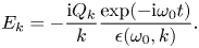
We use the source spatial distribution as in (2.10), whose Fourier transform is

Finally, to find $E(x)$ at $t\to +\infty$
 , we need to compute the inverse Fourier transform of $E_{k}$
 , i.e.

which can be done numerically. In § 5 this result is used for benchmarking our classical numerical simulations.
Appendix B. Laplace and Fourier transformation
For a given function $y(t)$ , we define the temporal Laplace transform as

where $\omega$ is a complex value such that ${\rm Im}\,\omega$
 is large enough for the integral to converge. Accordingly, the Laplace transform of the time derivative of $y$
 can be written as
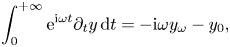
where we integrated by parts and introduced $y_0 = y(t=0)$ . The Laplace transforms of higher-order derivatives are derived similarly.
The inverse Laplace transform is

In the inverse transformation, the integration contour goes along the axis $(-\infty +\mathrm {i} \gamma,+\infty + \mathrm {i}\gamma )$ with a positive $\gamma$
 such that all singularities of $y_\omega$
 lie below the axis. Provided that $y_\omega$
 is well behaved at ${\rm Im}\,\omega \to -\infty$
 and also that the only singularities of $y_\omega$
 are poles $\omega _j$
 , one can shift the integration contour downward in the complex-$\omega$
 plane while still encircling the poles from above. Then, the contribution from the horizontal part of the contour vanishes and only the pole contributions remain. In this case, the integral can be computed as a sum of residues at the function poles:

We define the Fourier transform of a given function $z(x)$ as
as
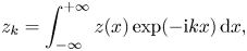
where $k$ is a real value. The inverse Fourier transform is then
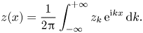
Appendix C. Supplemental gates
To encode the complex value $e_c = |e_c| \exp [\mathrm {i}\arg (e_c)]$ , we use the operator

with $\theta _z = - 2 \arg (e_c)$ and $\theta _y = 2 \arccos (|e_c|)$
 .
.
To shift an unsigned integer encoded in qubits by an integer more than $1$ , one can use the gates discussed in Novikau et al. (Reference Novikau, Dodin and Startsev2023), Suau et al. (Reference Suau, Staffelbach and Calandra2021) and Draper (Reference Draper2000). However, since here we need only shifts by ${\pm }1$
 , ${\pm }2$
 and ${\pm }3$
 , we introduce shorter circuits for these operations. The shift by ${\pm }1$
 corresponds to an incrementor or decrementor (figure 18). These operators are denoted as $A1$
 and $S1$
 , correspondingly, in figure 11. The shift by ${\pm }2$
 does not modify the least significant qubit and, therefore, corresponds to the incrementor or decrementor whose circuit is shifted upwards (figure 19). These operators are denoted as $A2$
 and $S2$
 , correspondingly. The circuit for the adder by $3$
 , shown in figure 20, can be understood as a combination of the circuits of an adder by $4$
 and a subtractor by $1$
 . The adder and subtractor by $3$
 are denoted as $A3$
 and $S3$
 , correspondingly. The number of STMC gates in all these operators scales as $\mathcal {O}(n)$
 .
.
The circuit of an incrementor, denoted as $A1$ , which acts on the target register $t$
 with $n$
 qubits. The circuit of a decrementor denoted as $S1$
 is inverse to the circuit shown here.
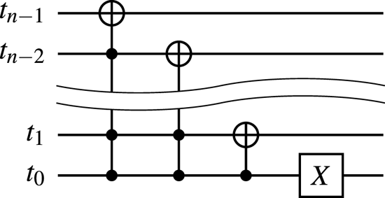
The circuit of an adder, denoted as $A2$ , which adds $2$
 to the unsigned integer encoded in the target register $t$
 with $n$
 qubits. The circuit of a subtractor by $2$
 , $S2$
 , is inverse to the circuit shown here.
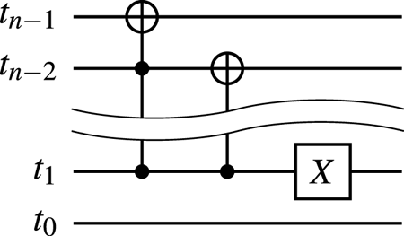
The circuit of an adder, denoted as $A3$ , which adds $3$
 to the unsigned integer encoded in the target register $t$
 with $n$
 qubits. The circuit of a subtractor by $3$
 , $S3$
 , is inverse to the circuit shown here.
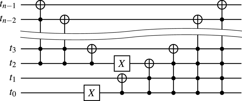


 Open access

