


Introduction
Recently, there are increasing concerns of sustainable energy and environment due to the growing consumption of non-renewable fossil fuels. The urgent requirement for clean and renewable energy sources has stimulated the rapid development of efficient, stable and reliable electricity supply systems. Lithium-ion batteries (LIBs) have been widely utilized in modern society such as in portable electronic device, electrical vehicles (EVs), and large-scale grid.[ Reference Armand and Tarascon 1 – Reference Mai, Tian, Xu, Chang and Xu 3 ] Recently, with the great concerns about the limited lithium (Li) resource, sodium-ion batteries (SIBs) have emerged as one of promising alternatives to LIBs due to its abundant and inexpensive sodium (Na) resource.[ Reference Slater, Kim, Lee and Johnson 4 , Reference Palomares, Serras, Villaluenga, Hueso, Carretero-González and Rojo 5 ] Meanwhile, Na has been studied to exhibit suitable redox potential and similar intercalation chemistry to Li; thus, SIBs hold promise to be viable complement or replacement to LIBs as the next-generation energy storage device.[ Reference Kim, Seo, Ma, Ceder and Kang 6 , Reference Ong, Chevrier, Hautier, Jain, Moore, Kim, Ma and Ceder 7 ] However, the larger radius of Na+ ions requires an expanding host space when a typical sodiation/desodiation process occurs. Consequently the size effect of Na+ ions would result in severe damage on the lattice structure of the host. Besides, Na+ ions are demonstrated to exhibit lower diffusion rate compared with Li+ ions. Therefore, the understanding and development of reliable cathode with suitable lattice space to host Na+ ions are the key issues to be addressed.
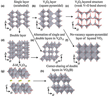
Vanadium oxides feature unique open-layered structures, which allow a diversity of other cations or molecules to insert into the layers.[ Reference Mai, Xu, Xu, Han and Luo 8 , Reference An, Lv, Liu, Han, Zhao, Sheng, Wei, Yan and Mai 9 ] In LIBs, these open-layered structures are capable to accommodate more Li+ ions, thus give rise to higher specific capacity than those of the commercial cathodes.[ Reference Murphy, Christian, DiSalvo and Waszczak 10 ] Moreover, vanadium oxides display rich redox chemistry due to different oxidation states and coordination geometries, therefore resulting in their different valence states and phase structures. With concerns to their layered structures, vanadium oxides generally contain [VO6] octahedral geometry with less [VO4] tetrahedron. Basically, these octahedral can form two-dimensional (2D) sheet structures by sharing edges and/or corners (sometimes faces).[ Reference Chernova, Roppolo, Dillon and Whittingham 11 ] These octahedral or tetrahedron possessed with a long V–O bond (2.1–2.6 Å, and 2.79 Å in V2O5 itself) and a short vanadyl bond, –V = O (1.55–1.75 Å) are capable to form various layered structures (Fig. 1). As depicted in literature, a double chain of edge-sharing [VO6] octahedral is the basic assembly unit. When the double chains are congregated by sharing the side corners, and a single layer can occur in most vanadium oxides [Fig. 1(a)]. In orthorhombic α-V2O5 [Fig. 1(b)], a short vanadyl bond and the other longer V–O bonds coexist. Consequently, the vanadium coordination polyhedron changes into a square pyramid due to the longer weak bond [weak V–O bond illustrated in Fig. 1(c)].[ Reference Chernova, Roppolo, Dillon and Whittingham 11 ] As suggested by Sohn et al., when these (V2O4) n chains closely aligned by sharing edges, no-vacancy square-pyramidal layered VO2 is formed [Fig. 1(f)].[ Reference Sohn, Joo, Ahn, Lee, Porter, Kim, Kang and Welland 12 ] V6O13 structure is formed by single and double layers sharing corners alternatively [Fig. 1(e)].[ Reference Wilhelmi, Waltersson and Kihlborg 13 ] When all the apices (vanadyl bonds) emerge up in one layer and also down in the other layers, a typical double layer of δ-type vanadium oxides can be created from single sheets [Fig. 1(g)]. To avoid confusion with double-sheet V2O5, this unique double layer of vanadium oxide is designated as δ-M x V4O10, which predominately exists in most of vanadium oxides gels.[ Reference Zavalij and Whittingham 14 ] When double layers of the δ-M x V4O10 structure collapse through the elimination of the interlayer species such as water molecule or metal ions, a metastable form of vanadium dioxide VO2(B) is constructed [Fig. 1(h)].[ Reference Oka, Yao, Yamamoto, Ueda and Hayashi 15 ]
Various layered vanadium oxide structures: (a) single layer of V2O5 (octahedral); (b) single layer of V2O5 (square pyramid); (c) layer structure of α-V2O5; (d) double layer of V2O5; (e) alternation single and double layer of V6O13; (f) no-vacancy square pyramidal layer of VO2; (g) structure of δ-M x V4O10; (h) corner sharing stacking of double layers in VO2(B). (Adapted/reproduced with permission from Ref. Reference Chernova, Roppolo, Dillon and Whittingham11, Royal Society of Chemistry, 2009.)
The sodiation/desodiation in vanadium oxide cathode are complex multi-electronic reaction processes. The applications of vanadium oxides in SIBs are restricted by rapid capacity fading caused by a decrease of the Na diffusion coefficient and severe structure deterioration. The concept of enhancing Na storage performance via nanostructuring has been recognized in numerous research works.[ Reference Jian, Han, Lu, Yang, Hu, Zhou, Zhou, Li, Chen, Chen and Chen 16 – Reference Raju, Rains, Gates, Luo, Wang, Stickle, Stucky and Ji 20 ] These novel nanostructures are proved to possess robust structural integrity and stability, faster electrochemical reaction rate, and enhanced reaction reversibility. In this perspective, we provide a brief review of recent advances in several typical vanadium oxides, and discussions on the engineering of unique nanostructures and its beneficial effects on enhancing the SIBs performance. Some intriguing and insightful studies of in situ X-ray diffraction (XRD) characterization on vanadium oxides for SIBs will be provided. Finally, perspective outlooks will be carefully addressed based on recent advances on the construction and understanding of nanostructured layered vanadium oxide for high-performance SIBs cathode.
Electrochemical performance of layered vanadium oxide cathode for SIBs
Binary vanadium oxide
In general, large families of vanadium oxides include binary vanadium oxides (containing V and O elements exclusively) and multicomponent vanadium oxides. Firstly, we briefly provided representative recent advances of the layered binary vanadium oxides cathode systems, together with their electrochemical cycling data for SIBs, as summarized in Table. 1.
Summary of representative recent advances of the binary layered vanadium oxides (containing V and O elements exclusively) cathode systems, together with their electrochemical cycling data for SIBs.

VO2
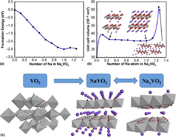
VO2 have been reported to exist in dozens of different phases species with their particular structural characteristics.[ Reference Mai, Wei, An, Tian, Zhao, Xu, Xu, Chang and Zhang 21 , Reference Baudrin, Sudant, Larcher, Dunn and Tarascon 22 ] Among these known phases, metastable VO2(B) exhibits layered structure to allow the intercalation of guest ions for high-performance SIBs. Various novel VO2(B) nanostructures have been reported, such as VO2(B) nanospheres,[ Reference Li and Liu 23 ] nanowires,[ Reference Zhang, Zhao, Xu, Meng, He, An, Xu, Luo, Zhao and Mai 24 ] nanosheets,[ Reference Nethravathi, Rajamathi, Rajamathi, Gautam, Wang, Golberg and Bando 25 ] nanowires assembled hollow spheres,[ Reference Niu, Meng, Han, Zhao, Yan and Mai 26 ] and micro/nano-structured nanoparticles.[ Reference Uchaker, Gu, Zhou, Li, Wang and Cao 27 ] It should be noted that, in a typical heat treatment or solution reaction process, VO2(B) trends to transform into monoclinic phase VO2(M) and tetragonal phase VO2(R), which barely exhibit electrochemical activity. Therefore, the controllable synthesis of pure phase VO2(B) is critical for its good electrochemical performance. Jiao and co-workers for the first time synthesized single-crystalline VO2(B) parallel ultrathin nanosheets for the cathode material in SIBs via a simple hydrothermal method.[ Reference Wang, Jiang, Hu, Lin, Hou and Jiao 28 ] As the number of the inserted Na+ ions increases from 0 to 1.0, the formation energy gets lower, implying the formation of the more stable phase. As the number of inserted Na+ ions excess 1.0, the formation energy of Na x VO2 becomes more positive compared with NaVO2, and on this occasion, the discharge process cannot take place spontaneously [Fig. 2(a)]. As they indicated that when the number of inserted Na+ ions per formula increases from 0.25 to 1, the interlayer distance changes a little. For more Na ions inserted into the tunnels (x > 1), the cell volume begins to expand consecutively. The backbone of the V–O tunnels is completely broken down and the stability and reversibility of the VO2-like structure are destroyed [Fig. 2(b)]. The proposed reaction mechanism can be illustrated as VO2 + xNa+ + xe− ↔ Na x VO2 [Fig. 2(c)] based on their findings.
(a) The relationship between the formation energy and the number of Na ions in Na x VO2. (b) Volume with respect to the number of Na ions in a VO2 molecule. (c) Schematic illustration of Na ions insertion and extraction process. (Adapted/reproduced with permission from Ref. Reference Wang, Jiang, Hu, Lin, Hou and Jiao28, Elsevier, 2014.)
The weak Na+ ions transport kinetics has been considered as the major drawback of cathode electrode for SIBs. Nanoscale surface engineering has significant effects on promoting the reaction kinetic of battery electrode. Chao et al. reported a binder-free cathode composed of VO2 arrays directly growing on graphene networks for SIBs cathode [Figs. 3(a)–3(f)].[ Reference Chao, Zhu, Xia, Liu, Zhang, Wang, Liang, Lin, Zhang and Shen 29 ] The integrated electrode delivers a capacity of 306 mA h/g at 100 mA/g, and a capacity of more than 110 mA h/g after 1500 cycles at 18 A/g [Fig. 3(g)]. Furthermore, at the ultrahigh rate of 120 C, the power density based on mass of the whole electrode is as high as 42 kW/kg with an energy density of more than 100 W h/kg [Fig. 3(h)]. Tong and co-workers also reported an unique free-standing cathode consisted of carbon quantum dots coated VO2 nanowires.[ Reference Balogun, Luo, Lyu, Wang, Yang, Li, Liang, Huang, Huang and Tong 30 ] The carbon quantum dots, which are flexible for surface engineering can efficiently ensure the integrity of nanowire. Another interesting work demonstrates the facile microwave-assisted solvothermal method to fabricate VO2(B)/ reduced graphene oxide (rGO) with good Na storage performance.[ Reference He, Li and Manthiram 31 ] The phase amorphization of VO2 when potential bellows 0.5 V confirmed some stable metal oxides might display better behavior in SIBs than expected.
(a–c) Fabrication process of GF supported GQDs-coated VO2 nanobelts array, (d–f) the corresponding SEM images in each process, respectively. (g) Cycling performance of the three electrodes at 60 C for 1500 cycles (1/3 C at the first five cycles for activation); (h) Ragone plot based on the total mass of the whole electrode, the sloping lines indicate the relative time to get the charge in or out of the electrodes. (Adapted/Reproduced with permission from Ref. Reference Chao, Zhu, Xia, Liu, Zhang, Wang, Liang, Lin, Zhang and Shen29, American Chemical Society, 2015.)

Orthorhombic V2O5
With respect to orthorhombic V2O5, a storage mechanism was proposed by Chung and co-workers that the appearance of NaV2O5 was a major phase with minor Na2V2O5 when fully discharged.[ Reference Ali, Lee, Oh, Cho, Nam and Chung 32 ] Their synchrotron based near edge X-ray adsorption fine structure (NEXAFS) spectroscopy results also suggested the charge compensation during desodiation/sodiation process accomplished by the reversible changes between V4+↔ V5+. As for the Na storage performance of α-V2O5 cathode, the major issue hinders the performance caused by the slow Na ion diffusion. Therefore, the controllable synthesis of α-V2O5 electrode materials with versatile nanostructures plays an important role for achieving good electrochemical performance. Ji and co-workers reported an orthorhombic V2O5 coated inside nanoporous carbon composite for SIBs cathode. For the first time they demonstrated that this composite displays superior Na storage performance [Figs. 4(a) and 4(b)],[ Reference Raju, Rains, Gates, Luo, Wang, Stickle, Stucky and Ji 20 ] and a capacity of over 90 mA h/g at a current rate of 640 mA/g [Fig. 4(c)]. They also demonstrated V2O5 pseudocapacitance contributes to a large portion of the Na storage especially under high current rates operating condition [Figs. 4(d) and 4(e)].
(a) HAADF-STEM image of V2O5-nanoporous carbon (RFC) and the corresponding EDX mappings of (b) vanadium; (c) Galvanostatic charge−discharge profiles of 55-V2O5-RFC at various current densities. (d) CV profiles of 55-V2O5-RFC at different scanning rates from 0.5 to 10 mV/s. (b–e) CV profile for 55-V2O5-RFC at a sweeping rate of 5 mV/s. The estimated capacitive current contribution is shown in the shaded region. (Adapted/Reproduced with permission from Ref. Reference Raju, Rains, Gates, Luo, Wang, Stickle, Stucky and Ji20, American Chemical Society, 2014.) (f) FESEM image of V2O5 nanospheres. (g) FFT pattern along the (110) zone axis of V2O5 and inset in the middle of (g) is the simulated V2O5 (110) crystal plane. (h) Rietveld refinement pattern of XRD data for V2O5 nanospheres. The observed and calculated intensities are represented by red crosses and the blue solid line, respectively. (i) 1st, 2nd, 3rd, and 100th cycle discharge and charge profiles of V2O5 hollow nanospheres at 20 mA/g current density. (Adapted/reproduced with permission from Ref. Reference Su, Dou and Wang33, Royal Society of Chemistry, 2014.)

Void architecture and exposed crystal planes of V2O5 nanocrystals have been confirmed to enhance good high-rate capability and cycling stability of α-V2O5. Wang and co-workers synthesized hollow orthorhombic V2O5 hierarchical nanospheres through a polyol-induced template-free solvothermal approach [Fig. 4(f)].[ Reference Su, Dou and Wang 33 ] Transmission electron microscopy (TEM) [Fig. 4(g)] and refined XRD analyses [Fig. 4(h)] revealed that the V2O5 hollow nanospheres were composed of hierarchical nanocrystals and most of these nanocrystals exhibit exposed {110} crystal planes. V2O5 hollow nanosphere shows a high initial discharge capacity of 223 mA h/g; however, only 159 mA h/g discharge capacity is obtained after the second cycle. The achieved capacity is equal to the intercalation of one Na ion for each formula unit to form a crystal structure of NaV2O5 [Fig. 4(i)].
Bilayered V2O5
Bilayered V2O5 has attracted much interest due to its larger interlayer distance compared to that of aforementioned α-V2O5. Rajh and co-workers found that bilayered V2O5 stacks are split up by large interlayer spacing, which is evidenced by as a broad strong peak at high d spacing (~13.5 Å), confirmed by X-ray scattering [Figs. 5(a) and 5(b)] and TEM results [Figs. 5(c)–(e)].[ Reference Tepavcevic, Xiong, Stamenkovic, Zuo, Balasubramanian, Prakapenka, Johnson and Rajh 34 ] Notably, bilayered V2O5 undergoes an entirely different intercalation mechanism compared to orthorhombic V2O5. Two phase transitions have been discovered when Na+ ions incorporate into the orthorhombic electrode, implying that the orthorhombic crystalline structure changes two times to accommodate increased concentration Na+ ions. In contrast, no phase transitions occur when Na+ ions intercalate into bilayered V2O5, revealed by the representative smooth, solid state solution intercalation profiles [Fig. 5(f)]. Notably, the crystallinity of the materials does not degenerate during cycling and the sample maintains stable crystalline structure after 80 cycles [Fig. 5(g), red curve]. In a word, the intercalation of Na+ ions causes arrangement of structure to possess both long- and short-range order; whereas the deintercalation process results in the loss of long-range order and the retention of short-range order [Fig. 5(h)].
XRD patterns, SEM images and the molecular simulations based on the monoclinic bipyramid layer structure model of (a) bilayered and (b) orthorhombic V2O5; (c, d) HRTEM images, and (e) SAED pattern of bilayered-V2O5; (f) Charge and discharge curves of first four cycles of bilayered-V2O5 and α-V2O5 electrodes at the current density of 20 mA/g; (g) Synchrotron XRD spectra of bilayered V2O5 annealed in vacuum at 120 °C (blue), in discharge after Na+ ion intercalation (black) and in charged state after Na+ ion deintercalation (red). (h) SAXS and WAXS spectra for bilayered V2O5 for as-deposited, in discharge and charged state. (Adapted/reproduced with permission from Ref. Reference Tepavcevic, Xiong, Stamenkovic, Zuo, Balasubramanian, Prakapenka, Johnson and Rajh34, American Chemical Society, 2012.)

Besides, more articles also reported high-performance bilayered V2O5 cathode for SIBs with controllable nanostructures, such as single-crystalline bilayered V2O5 nanobelts,[ Reference Su and Wang 35 ] sponge-like layered V2O5 nanosheets.[ Reference Zhu, Zhang, Guo, Yu, Liao, Chen, Wei and Zhou 36 ] A large (001) interlayer spacing (~11.53 Å) of V2O5 nanobelts can accommodate Na-ion intercalation and deintercalation. Interestingly, the unique bilayered vanadium oxide nanobelts were revealed to possess predominantly exposed {100} crystal planes, which offer large interlayer spacing for facile Na extraction/insertion.[ Reference Su and Wang 35 ]
V2O5·nH2O
The reduced structural order, the large interlayer space and the short diffusion length are the key factors that allow V2O5·nH2O to reversibly host cations.[ Reference McNulty, Buckley and O'Dwyer 37 , Reference Giorgetti, Passerini, Smyrl and Berrettoni 38 ] Recently, Moretti and Passerini provided a comprehensive review on bilayered nanostructured V2O5·nH2O for metal batteries, which confirms the renewed interests on V2O5·nH2O for energy storage.[ Reference Moretti and Passerini 39 ] Briefly, V2O5·nH2O can be obtained in xerogel or aerogel depending on different drying methods. This unique V2O5·nH2O is a representative class of δ-M x V4O10 [Fig. 1(g)] where water molecules intercalate and regular the layer spacing.[ Reference Petkov, Trikalitis, Bozin, Billinge, Vogt and Kanatzidis 40 ]
A variety of methods to prepare V2O5·nH2O as thin film or bulk powder have been developed. Among them, vapor deposition (physical or chemical) and solution methods draw great interests due to their facility and versatility. For example, Passerini and co-workers employed supercritical fluid (CO2) extraction to eliminate the water in V2O5 and fabricate a porous aerogel V2O5·nH2O (n = 2.1) [Fig. 6(a)].[ Reference Moretti, Maroni, Osada, Nobili and Passerini 41 ] When applied as a SIBs cathode, high specific capacities were achieved due to its open framework with expanded interlayer spacing and decreased diffusion path [Fig. 6(b)]. Mai and co-workers developed a facile freeze-drying process to synthesize a V2O5·nH2O xerogel composed of thin interconnected nanowire networks [Fig. 6(c)].[ Reference Wei, Liu, Feng, Sheng, Tian, He, An and Mai 42 ] Ex situ XRD indicated the layer of V2O5·nH2O is shrinking/expanding accompanied by the Na+ ion insertion/extraction, which is different from the irreversible phase transition of α-V2O5 [Figs. 6(d) and 6(e)]. Ex situ Fourier transform infrared spectroscopy (FTIR) results demonstrated that the crystal water is not completely replaced during Na+ ion insertion [Fig. 6(f)]. To improve its stability, iron preintercalated vanadium oxide ultrathin nanobelts (Fe-VO x ) with constricted interlayer spacing were fabricated.[ Reference Wei, Jiang, Tan, Li, Huang, Yan, Zhou, An and Mai 43 ] The electrochemical performances of V2O5·nH2O have been enhanced via electrolyte optimization[ Reference Moretti, Jeong and Passerini 44 ] or cut-off voltage,[ Reference Moretti, Secchiaroli, Buchholz, Giuli, Marassi and Passerini 45 ] even though long-term cycling stability still need to be addressed.
(a) SEM image of dried V2O5 powder; (b) Cycling behavior of V2O5 electrodes at high current densities. (Adapted/reproduced with permission from Ref. Reference Moretti, Maroni, Osada, Nobili and Passerini41, Wiley, 2015.) (c) SEM image of V2O5·nH2O xerogel. (d) Ex situ XRD patterns (e) related d 001 value changes. (f) FTIR spectra of the V2O5·nH2O xerogel cathodes in the SIB. (Adapted/Reproduced with permission from Ref. Reference Wei, Liu, Feng, Sheng, Tian, He, An and Mai42, Journal of Materials Chemistry A, Royal Society of Chemistry, 2015.)

Amorphous V2O5
Amorphous electrode materials have received considerable interests as they can reduce the stress and might provide isotropic transport path for ions compared with crystalline materials.[ Reference An, Lv, Liu, Han, Zhao, Sheng, Wei, Yan and Mai 9 , Reference Sun, Zhou, Xie, Hu, Sun, Xin, Wang, George and Lian 46 ] As exemplified in some reports, some amorphous aerogels or xerogel prepared are featured with low density, highly porous and high surface area and are being explored as new promising materials in electrochemistry.[ Reference Sheng, Li, Wei, Zhang, Wang, Lv, An, Chen and Mai 47 – Reference Rolison and Dunn 51 ] Gao et al. demonstrated amorphous V2O5 exhibited superior Na storage performance compared with its crystalline counterpart.[ Reference Uchaker, Zheng, Li, Candelaria, Hu and Cao 52 ] No distinctive peak can be observed when the cyclic voltammetry (CV) scan was conducted on this amorphous V2O5, however the current response was scaled with the potential and was even greater than that of the crystalline counterpart. The less ordered and abundant open channels decrease the diffusion barrier for Na+ ions to transport, which contribute to high-rate capability and high-energy density. The amorphous matrix makes it easier for Na+ ions to intercalate into the crystal and diffuse deeper into the host material. Due to the isotropic penetration pathway of ions rather than some certain preferential directions, the overall charging–discharging rates are much faster, as evidenced by a capacity of 78 mA h/g at a current density of 1180 mA/g. Recently, Li and co-workers demonstrated that amorphous V2O5 cathode possesses higher reversible capacities than the crystalline V2O5 at low-current densities, whereas it is inversed at high current densities.[ Reference Liu, Tong, Zhao, Liu, Wang, Ma, Chi, Yang, Liu and Li 53 ] Therefore, the rational selection of amorphous or crystalline V2O5 cathode for SIBs need to be further investigated with respects to various operation requirements.
Layered-structured vanadate compounds
Layered-structured vanadates are studied as typical layered vanadium oxides incorporating second metals such as Li, Na, or transition metals such as cobalt, silver, and iron. In this short perspective article, we will focus on the classic intensively studied Na3V2(PO4)3 (NVP) composites and emerged promising K3V2(PO4)3 composites in this group and get inspiration upon the investigation of other vanadate compounds.
Na3V2(PO4)3
Among the big family of vanadium compounds, NVP have been intensively studied as SIBs cathodes because of its high theoretical capacity and stable Na super ion conductor (NASICON) structure.[ Reference Jian, Yuan, Han, Lu, Gu, Xi, Hu, Li, Chen and Chen 54 – Reference Shen, Li, Guo, Wang, Li, Xu, Liu, Wang and Xia 59 ] Especially, NVP displays two potential plateaus located at 3.4 and 1.6 V versus Na/Na+, related to the V3+/V4+ and V2+/V3+ redox couples, respectively.[ Reference Saravanan, Mason, Rudola, Wong and Balaya 55 ] These two reactions can provide a specific capacity of approximately 117 and 50 mA h/g at the high- and low-voltage zones, respectively. Since the first report on superior electrochemical performance and storage mechanism of NVP cathode for room-temperature SIBs,[ Reference Jian, Han, Lu, Yang, Hu, Zhou, Zhou, Li, Chen, Chen and Chen 16 ] numerous literatures demonstrated the great advances in performance enhancement and mechanism investigation, which cannot be totally included in this perspective. Herein some great advances are exemplified subsequently. Carbon or graphene modification has been proven as an efficient strategy to improve conductivity and rate capability. A hierarchical carbon framework wrapped NVP composite is fabricated via chemical vapor deposition on NVP particles.[ Reference Fang, Xiao, Ai, Cao and Yang 60 ] The NVP hybrid electrode can exhibit a high reversible capacity of 115 mA h/g at 0.2 C and long-term cycling stability (a capacity retention of 54% after 20,000 cycles). Mai and co-workers designed a novel synthesis of layer-by-layer NVP@ rGO nanocomposite by adjusting the surface charge of NVP gel precursor [Fig. 7(a)].[ Reference Xu, Wei, Xu, Li, An, Zhang, Sheng, Zhou and Mai 61 ] The NVP@rGO nanocomposite contains trace amount of rGO and amorphous carbon, yet displays superior electrochemical performance [Fig. 7(b)]. The morphological optimization of NVP material has a great significance for improving the electrochemical performance since NVP suffers from intrinsic low electronic conductivity. For this purpose, Mai and co-workers introduced a novel 3D NVP nanofiber network controllably constructed via a facile self-sacrificed template method.[ Reference Ren, Zheng, Xu, Niu, Wei, An, Zhao, Yan, Qin and Mai 62 ] The as-synthesized material displays excellent cyclability (95.9% capacity retention over 1000 cycles at 10 C) and enhanced high-rate performance (94 mA h/g at 100 C) for Na half-cell. Notably, when evaluated as full battery [NaTi2(PO4)3 as anode] cathode, it also shows outstanding cycling stability (96.9% capacity retention over 300 cycles at 5 C) and superior rate capability (80 mA h/g at 50 C). Such remarkable performance is attributed to the 3D nanofiber network structure, which provides multi-channel ionic diffusion pathway, continuous electronic conduction, and improved structural integrity.
(a) TEM image of Na3V2(PO4)3@rGO; (b) ultraong cycling stability of the Na3V2(PO4)3@rGO for 15,000 cycles at a high rate of 50 C. (Adapted/reproduced with permission from Ref. Reference Xu, Wei, Xu, Li, An, Zhang, Sheng, Zhou and Mai61, Wiley, 2016.) (c, d) HRTEM images of the K3V2(PO4)3/C bundled nanowires; (e) rate performance of the K3V2(PO4)3/C bundled nanowires and blocks. (Adapted/reproduced with permission from Ref. Reference Wang, Niu, Meng, Hu, Xu, Wei, Zhou, Zhao, Luo, Yan and Mai63, Wiley, 2015.)

K3V2(PO4)3
Apart from intensively researched Na vanadates, a new type of potassium phosphate material K3V2(PO4)3, was designed for the first time and explored for Na storage by Mai et al.[ Reference Wang, Niu, Meng, Hu, Xu, Wei, Zhou, Zhao, Luo, Yan and Mai 63 ] K3V2(PO4)3/C bundled nanowires were fabricated through a simple organic acid-assisted approach [Figs. 7(c) and 7(d)]. Beneficial from a stable framework, nanoporous structure, and conductive carbon coating, the K3V2(PO4)3/C bundled nanowires cathode displays good electrochemical performances in SIBs. A capacity of 119 mA h/g can be achieved at a current density of 100 mA/g and K3V2(PO4)3/C bundled nanowires exhibit enhanced electrochemical performance compared to bulk KVP at various current densities [Fig. 7(e)].
In situ characterization of layered vanadium oxide cathode
In situ characterization has been recognized as a powerful tool to provide deeper and more direct insights into the materials degradation and phase transformation mechanisms under real-time working condition.[ Reference Ma, Luo, Yan, He and Mai 64 – Reference Lu, Adkins, He, Zhong, Luo, Mao, Wang and Korgel 66 ] The comprehensive understanding of morphological and microstructural changes of layered vanadium oxide cathode during charge and discharge processes are essential for the improving of the electrochemical performance.[ Reference Niu, Liu, Meng, Xu, Yan, Wang, Zhang, Liu, Xu and Mai 67 , Reference Liu, Liu, Kushima, Zhang, Zhu, Li and Huang 68 ] Some advances on in situ XRD characterization of vanadium oxide cathode will be discussed to emphasize its importance and arouse broad research interests. For more knowledge on in situ characterization on energy storage materials, readers can be referred to some specific reviews.[ Reference Ma, Luo, Yan, He and Mai 64 ]
Delmas and co-workers firstly present the detailed phase diagram and in situ XRD experiments of the layered P2-Na x VO2 system for electrochemical Na insertion/extraction in SIBs.[ Reference Guignard, Didier, Darriet, Bordet, Elkaïm and Delmas 69 ] Notably, four predominate single phase can be detected within the 0.5 ≤ x ≤ 0.9 range [Figs. 8(a) and 8(b)]. During the Na insertion/extraction, they exhibit different Na/vacancy ordering between the VO2 layers, which results in comparable or unmatched superstructures. Na+ ions are found to perfectly order to minimize Na+/Na+ electrostatic repulsions [Fig. 8(c)]. Within the VO2 layers, the vanadium ions tend to form pseudo-trimers possessing extremely short V–V distances (two at 2.581 Å and one at 2.687 Å) [Figs. 8(d) and 8(e)]. More importantly, this phase exhibits a first-order structural transition beyond room temperature along with noticeable electronic and magnetic transitions. This work for the first time gets a precise study of phase diagram of this system in SIBs at room temperature, associated with in situ XRD experiments, and highlights the importance and powerfulness of in situ characterization combined with suitable simulation techniques.
(a) Evolution of cell voltage as a function of Na content in Na x VO2 over the 0.5 ≤ x ≤ 0.92 range; (b) In situ XRD data recorded during the galvanostatic intermittent titration technique experiments. (c) Synchrotron diffraction pattern of P2-Na1/2VO2 and Rietveld refinement of its structure. (d–f) Projection of the structure of P2-Na1/2VO2 along the c-axis. (Adapted/reproduced with permission from Ref. Reference Guignard, Didier, Darriet, Bordet, Elkaïm and Delmas69, Nature Publishing Group, 2012.)

In situ XRD characterization can also provide detailed structure information for new-type vanadium oxide cathode candidates for SIBs. Mai et al. employed a new-type K3V2(PO4)3/C as cathode materials for SIBs.[ Reference Wang, Niu, Meng, Hu, Xu, Wei, Zhou, Zhao, Luo, Yan and Mai 63 ] Through in situ XRD investigation, the intensity and position of peak shifted during the charge and discharge reversibly, corresponding to the (de)insertion of K+/Na+ and the expansion/extraction of the lattice distance [Figs. 9(a) and 9(b)]. The vanadium phosphate showed excellent stability, which allows the deinsertion of K+ ion and insertion of Na+ ion without collapse of crystal structure.
(a) The image plot of the diffraction patterns at 23–27° and 30–34° during the first two charge–discharge cycles of K3V2(PO4)3/C bundled nanowires. (b) Selected diffraction patterns during the first cycle stacked against the voltage profile. (Adapted/reproduced with permission from Ref. Reference Wang, Niu, Meng, Hu, Xu, Wei, Zhou, Zhao, Luo, Yan and Mai63, Wiley, 2015.) (c) Crystal structure of Na3V2(PO4)3 (NVP); (d) The in situ XRD patterns of NVP for a full charge–discharge cycle; (e) The corresponding time–potential curve. (Adapted/reproduced with permission from Ref. Reference Ren, Zheng, Xu, Niu, Wei, An, Zhao, Yan, Qin and Mai62, Elsevier, 2016.)

Beside, in situ XRD characterizations are capable to offer direct observation on crystal structure evolution of cathode material during Na+ ions insertion/deinsertion process. The prepared NVP nanofiber in situ cell was charged to 3.9 V and then discharged to 2.3 V. All the Na3−α V2(PO4)3 peaks disappear on charge and are restored on discharge; Conversely, Na β V2(PO4)3 peaks start to form and grow on charge and disappear on discharge [Figs. 9(d) and 9(e)].[ Reference Ren, Zheng, Xu, Niu, Wei, An, Zhao, Yan, Qin and Mai 62 ] It is clear that the (211) and (300) peaks shift to higher angles during charge process, indicating that the d-spacings decrease during the Na+ ions de-insertion. After recharging to 3.9 V, the peaks return to the original positions, indicating the good reversibility.
Summary and outlook
As discussed above, notable progress has been made on the synthesis of vanadium oxide for high-performance SIBs along with some in situ XRD characterizations to disclose its intrinsic Na storage mechanism. However, there are still big challenges to be faced. Some perspectives are carefully addressed here, and the future studies on vanadium oxide as SIBs cathode are suggested to be deliberately initiated in the following aspects:
-
(1) Developing facile, efficient, sustainable, and controllable synthesis of novel nanostructures. In terms of the controllable synthesis of vanadium oxide cathode for SIBs, nanoscience engineering makes it possible to control the morphology and composition of cathode to effectively enhance the electrochemical performance. Recently, numerous reported method can be applied to obtain diverse nanostructures (i.e., hollow structure,[ Reference Su, Dou and Wang 33 ] hierarchical heterostructures,[ Reference Dong, Li, Zhao, Han, Chen, Wang, Wang, Xu, Wei and Zhang 18 , Reference Wang, Zhao, Zhang, Gao and Deng 19 , Reference Fang, Xiao, Ai, Cao and Yang 60 ] complex 3D architectures,[ Reference Ren, Zheng, Xu, Niu, Wei, An, Zhao, Yan, Qin and Mai 62 ] etc.) with peculiar electrochemical properties, interlayer spaces and morphologies. However, some synthetic methods are generally time-consuming and danger-risking in which various sophisticated steps and/or toxic, expensive chemicals involve. At this stage, developing facile, efficient and controllable synthesis of novel vanadium nanostructures is still urgently demanded. Therefore, more efforts shall be addressed on the knowledge and capability to construct the desired nanostructure architectures based on a comprehensive understanding.
-
(2) Precisely designing and regulating layered structure with direct evidences. Normally, vanadium oxides feature rich redox chemistry due to different oxidation states and coordination geometries. The open framework facilitates ion movement, while the nanostructuring strategy can decrease the solid-state diffusion limitations and thus enhance the intercalation kinetics.[ Reference Wang and Cao 70 ] To name a few, preferentially exposed facets,[ Reference Su, Dou and Wang 33 , Reference Su and Wang 35 ] metal ions, or water molecule preintercalation[ Reference Wei, Liu, Feng, Sheng, Tian, He, An and Mai 42 , Reference Wei, Jiang, Tan, Li, Huang, Yan, Zhou, An and Mai 43 ] and the regulation of short-range order in layered structure[ Reference Tepavcevic, Xiong, Stamenkovic, Zuo, Balasubramanian, Prakapenka, Johnson and Rajh 34 ] show great interests upon high-performance vanadium layered oxides. Whereas how to accurately tune the lattice space and stabilize its layered structure for long-term cycle needs to be addressed. Moreover, intercalation chemistry opens up a possibility to explore potential new-type vanadium oxide host materials for SIBs, and challenges and breakthroughs might lie ahead bearing the deeper understanding of solid state physics.
-
(3) Gaining insights into mechanism via various modern techniques. With regards to in situ characterization of cathode for SIBs, the working mechanisms of novel vanadium oxide cathode and their designing principles need further investigations. More direct evidences showing the correlation between the structure of the vanadium oxide and the electrochemical performance are greatly needed. For instance, although in situ XRD characterization show great advantages in observing the structural evolution of some typical vanadium oxides and present the detailed phase diagram, some important characterization methods (e.g., atomic force microscopy) are absent. Recent advances in the disclosing the role of structural H2O in intercalation vanadium oxide are assisted by PDF (pair distribution function) analysis and/or DFT (density functional theory) calculations.[ Reference Shakoor, Seo, Kim, Park, Kim, Kim, Gwon, Lee and Kang 71 ] Intrinsic electrochemical mechanisms are expected to be addressed with the help of more advanced characterization instruments.[ Reference Ogata, Salager, Kerr, Fraser, Ducati, Morris, Hofmann and Grey 72 – Reference Shi, Ross, Zhao, Liu, Somorjai and Komvopoulos 74 ] The combination of novel nanostructure design and computational simulation may be a feasible way.
-
(4) Better understanding of amorphous layered vanadium oxides. Notably, some amorphous vanadium oxides are demonstrated to exhibit impressive Na storage performance. Such outstanding electrochemical performance can be attributed to the large amounts of disordered lattice vacancies as well as abundant defects within the amorphous materials.[ Reference Venkatesh, Pralong, Lebedev, Caignaert, Bazin and Raveau 75 ] It has been studied the introduction of defect favors the development of optimized intercalation compounds and leads to substantial improvements for energy storage applications.[ Reference Uchaker and Cao 76 ] Nevertheless, to monitor the lattice vacancy and defect as well as disclose the possible effects on electrochemical performance still remains as a big challenge. In an attempt to explore high-performance amorphous vanadium oxides for SIBs, new techniques and practical applications should be developed supported by numerous experimental and simulation results toward defects chemistry.
-
(5) Systematic and overall evaluation of the SIBs performance. Standardized methods for accurately characterizing the performance of full SIBs need to be established. Apparently, SIBs are indeed sophisticated systems associated with electrode structure, efficient electrolyte, packaging technology, and so forth. Comparing to the commercial LIBs, the development of high-efficiency electrolyte and separator, which are also vital for constructing high-performance vanadium oxide cathode-based full batteries, is insufficient. Currently, most reported research works on electrode materials have to conduct and present the optimization of electrolyte experiment for overall high-performance SIBs.[ Reference Komaba, Ishikawa, Yabuuchi, Murata, Ito and Ohsawa 77 – Reference Darwiche, Marino, Sougrati, Fraisse, Stievano and Monconduit 79 ] Besides, the rational choice of high-efficient binder and separator also highly depends on surface and interface chemistry knowledge.[ Reference Yuan, Huang, Ma, Wang, Meng and Zhang 80 , Reference Dahbi, Nakano, Yabuuchi, Ishikawa, Kubota, Fukunishi, Shibahara, Son, Cui and Oji 81 ] Thus, to establish reliable standard system is essential for the development of commercial SIBs. Na-ion related knowledge must be deeply explored to introduce new alternative energy storage systems in the near future. Opportunities exist for researchers to bring together chemistry, physics, and engineering in imaginative morphologies.
Acknowledgment
This work was supported by the National Key Research and Development Program of China (2016YFA0202603), the National Basic Research Program of China (2013CB934103), the Programme of Introducing Talents of Discipline to Universities (B17034), the National Natural Science Foundation of China (51521001), the National Natural Science Fund for Distinguished Young Scholars (51425204), and the Fundamental Research Funds for the Central Universities (WUT: 2016-JL-004, 2016III001 and 2017III009). Prof. Dr. Liqiang Mai gratefully acknowledged financial support from China Scholarship Council (Grant no. 201606955096).


