


Introduction
Ever since the introduction of atomic layer epitaxy by Suntola [Reference Puurunen1], numerous research on atomic layer deposition (ALD) have been conducted for a wide range of applications, including semiconductor applications in display, catalysis, functional coating, and medical and pharmaceutical applications [Reference Kim, Lee and Maeng2, Reference Meng, Yang and Sun3, Reference Skoog, Elam and Narayan4, Reference Singh, Lehnen, Leuning and Mathur5, Reference George6, Reference Park, Chae, Chung and Lee7, Reference Lu, Lei and Elam8, Reference Kim9, Reference Marichy, Bechelany and Pinna10, Reference Leskelä and Ritala11, Reference Kääriäinen, Kemell, Vehkamäki, Kääriäinen, Correia, Santos, Bimbo, Hirvonen, Hoppu, George, Cameron, Ritala and Leskelä12]. ALD is a self-limiting thin film deposition method based on surface-saturated reactions between chemical species, and it possesses a number of advantages when compared with other deposition methods (e.g., sputtering and CVD). These advantages are, for instance, the controllability of atomic-level thickness, excellent conformality, and large-area uniformity [Reference George6]. Although, owing to these advantages, ALD has become an indispensable technique for the fabrication of nanoscale devices, it was not in the spotlight when it was introduced due to low productivity. When scaling down of devices and thin film deposition of sub-nanometer thickness on a high-aspect-ratio substrate or 3D complex structure with excellent conformality were required, ALD became the main deposition technique for the fabrication of nanoscale devices. At the same time, many research groups tried to overcome the issue of low productivity by changing from a conventional temporal to a spatial ALD process [Reference Poodt, Cameron, Dickey, George, Kuznetsov, Parsons, Roozeboom, Sundaram and Vermeer13]. Owing to these numerous efforts, ALD has become one of the important deposition techniques in many industries.
From the recently published bibliometric analysis on ALD process, it can be seen that the number of publications on ALD has significantly increased from the early 2000s [Reference Alvaro and Yanguas-Gil14]. Metal oxides and nitride materials are the most studied materials among the reported ALD-grown materials. Deposition of metal oxides and nitrides using ALD is, therefore, the most prevalent, and this might be due to the importance of these materials for the fabrication of Si-based electronics, including gate dielectric [Reference Maeng, Park and Kim15, Reference Ye, Wilk, Kwo, Yang, Gossmann, Frei, Chu, Mannaerts, Sergent, Hong, Ng and Bude16, Reference Gusev, Cabral, Copel, D’Emic and Gribelyuk17] or diffusion barrier for interconnects [Reference Nam, Lee, Cheon, Lee, Kim, Kwon, Lee and Kim18, Reference Hong, Jung, Yeo, Cheon, Bae, Kim, Yeo, Kim, Chung, Park, Kim and Lee19, Reference Kim, Detavenier, Van Der Straten, Rossnagel, Kellock and Park20]. Some conductive oxides (e.g., ZnO and In2O3) have also been considered as transparent conductive oxides or channel materials in displays [Reference Lee, Kim, Kwon, Choi, Kim and Kim21, Reference Nam, Lee, Kim and Kim22, Reference Dasgupta, Neubert, Lee, Trejo, Lee and Prinz23, Reference Kim, Nam, Park, Gatineau and Kim24]. Tens of metal oxides, on the other hand, have been developed for functional coatings [Reference Lu, Liu, Greeley, Feng, Libera, Lei, Bedzyk, Stair and Elam25, Reference Lee, Yoon, Kim, Kang, Oh, Algadi, Al-Sayari, Shong, Kim, Kim, Lee and Lee26, Reference Jung, Cavanagh, Gedvilas, Widjonarko, Scott, Lee, Kim, George and Dillon27] and energy or environmental applications [Reference Meng, Yang and Sun3, Reference Singh, Lehnen, Leuning and Mathur5, Reference Marichy, Bechelany and Pinna10]. In addition, various metals have been studied for the purpose of diffusion barrier, seed/adhesion layer, catalyst, and ultrathin conductive coating [Reference Leskelä and Ritala11, Reference Lee, Yoon, Kim, Kang, Oh, Algadi, Al-Sayari, Shong, Kim, Kim, Lee and Lee26, Reference Li, Gordon, Farmer, Lin and Vlassak28, Reference Christensen, Feng, Libera, Guo, Miller, Stair and Elam29]. Even though a number of materials have been developed for diverse applications, most research still focus on a limited number of materials, which may be due to the lack of need for new materials or precursors for deposition. As new concepts have been developed for improving processing and devices, such as hard mask for multiple patterning [30, Reference Yaegashi, Oyama, Hara, Natori and Yamauchi31, Reference Kim, Chung, Park, Lee, Yeo and Kim32], secure memory storage fabrication [Reference Yamahata, Shigekawa, Kurishima and Matsuoka33, Reference Choi, Jung, Lee, Mun, Kim, Park and Kim34], or neuromorphic devices which can overcome the current limitation of Si-based devices [Reference Ge, Wu, Kim, Shi, Sonde, Tao, Zhang, Lee and Akinwande35, Reference Sangwan, Lee, Bergeron, Balla, Beck, Chen and Hersam36, Reference Lee, Park, Kim, Im, Shin, Kim, Mohammad, Kang and Lee37], it is highly desirable to develop a nonconventional material deposition process based on ALD.
In this review, growth of nonconventional materials that have been rarely studied with ALD will be highlighted. We will discuss the recent progress of growing amorphous carbon (a-C), germanium oxide (GeO2), and 2D transition metal dichalcogenides (2D TMDCs) by the ALD process. These materials have been highlighted recently as new concepts for processing and emerging devices. We will briefly describe the need for these materials at the beginning of each section, followed by recent progress and outlook.
Recent progress on nonconventional material deposition using ALD
Amorphous carbon
Carbon is one of the most common elements on earth, and it exists in various forms by bonding with each other in different ways, known as allotropes of carbons [Reference Alvaro and Yanguas-Gil14]. There are many different types of carbon allotropes, and they show considerably different characteristics. These characteristics are comparable to those of the allotropes of other elements [Reference Hirsch38, Reference Milne and Robertson39, Reference Robertson40]. Diamond, for instance, one of the well-known allotropes of carbon with sp 3 configuration, is mainly used in industry for grinding or polishing, owing to its superior hardness from its bonding configuration [Reference Geim and Novoselov41, Reference Tillmann42]. Graphite is a crystalline form of carbon arranged in a hexagonal structure with 3-fold coordinated sp 2 configuration. Most of the carbon species exist as graphite under standard condition, showing high stability. Due to its high conductivity and excellent stability, graphite is frequently used as electrodes for batteries or refractory material [Reference Robertson40, Reference Mcenaney43]. Graphene, which has been recently discovered as another allotrope of carbon with 2D honeycomb structures, shows excellent electrical conductivity, even though the thickness of the material is less than a nanometer [Reference Geim and Novoselov41]. Carbon-based materials, therefore, show diverse characteristics depending on their structures, which can be applicable to various applications, especially when we can modulate the crystal structures of carbon.
a-C, a randomly hybridized carbon with sp 3 and sp 2 configurations, is one of the most fascinating materials for the hard mask for multiple patterning processes [Reference Electron and Society44, Reference Liu, Mui, Lill, Wang, Bencher, Kwan, Yeh, Ebihara and Oga45, Reference Park, Lee, Cho, Choi, Lee, Yoo, Shin, Min, Kang, Cho and Moon46], owing to its etch selectivity, hardness, and cost-effectiveness. As devices are being scaled down, photolithography encounters the physical limitation for sub-40 nm device fabrication [Reference Wagner and Harned47, Reference Tallents, Wagenaars and Pert48]. This limitation can be overcome by changing the light source to extreme ultraviolet (EUV), which enables the resolution of patterning below 10 nm. However, because of technical immaturity and poor cost-effectiveness, multiple patterning has been adapted on sub-20 nm device patterning, instead of EUV lithography [30]. Double patterning, one of the multiple patterning processes that were initially adopted, forms a fine pattern by patterning the same pitch twice, making a pattern size in half. In this patterning process, a-C is an essential material since a-C hard mask can resist any dry etch chemistry during the multiple patterning process with its superior etch selectivity, and it can be simply removed by oxygen plasma ashing without leaving behind any residue [Reference Horn, Annual, Le, Ngine, Conf and Nce49, Reference Ho, Lin, Chien and Lien50, Reference Pears51, Reference Kakuchi, Hikita and Tamamura52]. Currently, most of the a-C deposition is conducted by plasma-enhanced chemical vapor deposition (PE-CVD), which ensures high-throughput [Reference Liu, Mui, Lill, Wang, Bencher, Kwan, Yeh, Ebihara and Oga45, Reference Pears51]. As technology node decreases to the sub-10-nm scale, a further complex patterning process, i.e., quadruple, sextuple, or octuple patterning, is required [Reference Chen, Cheng and Kang53, Reference Bhushan54], and a deposition technique that ensures excellent conformality on the high-aspect-ratio structure spacer is needed for a-C deposition.
To obtain a single-element material using an ALD process, all ligands of the precursor core metal should be detached by the reaction with surface reactive species or subsequent reducing agents. In the early 2000s, Rossnagel and Kim reported a plasma-enhanced ALD (PE-ALD)–based Ta and Ti deposition using halide precursors and hydrogen radicals [Reference Rossnagel, Sherman and Turner55, Reference Kim and Rossnagel56]. In these studies, hydrogen radicals generated by H2 plasma have been suggested as promising reactants for single element deposition because of the high reducing ability of the hydrogen radicals. Even though the hydrogen radicals have excellent reactivity, a proper precursor selection is still important for a single-element material deposition using ALD. In these reports, a reaction between halide ligands and hydrogen radicals was available because of the high reactivity of halide ligands, forming volatile H–X by-products, where X is a halide [Reference Knoops, Potts, Bol and Kessels:57]. The bond dissociation energy is dependent on the ligand, and that means the external energy (e.g., heat) for the detachment of precursor ligands by hydrogen radicals could be increased, resulting in a high process temperature [Reference Matta, Castillo and Boyd58, Reference Michael, Lim, Kumaran and Kiefer59, Reference Kime, Driscoll and Dowben60, Reference Paddison and Tschuikow-Roux61]. Although the reaction energy is not directly related to the bond dissociation energy, a comparison with the energy required to dissociate a given species is still meaningful. In addition, some of the halide compounds that are formed during the reaction show stability at room temperature, hindering the adsorption of the subsequent precursors or reactants [Reference Park, Oh, Lee, Lee, Shin, Lansalot-Matras, Noh, Kim and Lee62]. For these reasons, it is critical to choose an adequate precursor whose ligand can be detached at a relatively low temperature without leaving any by-products on the surface. Thus, the selection of the precursor with adequate ligands is important to obtain pure single-element material deposition by ALD.
There have been only a couple of reports on carbon deposition using the ALD method. Hukka et al. reported a radical-enhanced ALD of carbon on a diamond substrate using chlorocarbon radicals, which were generated from a CHCl3 and H2 mixture, as a precursor and atomic hydrogen as a reactant from 850 to 950 °C [Reference Hukka, Rawles and D’Evelyn63]. Komarov et al. also reported radical ALD-based carbon on a Mo substrate using CFx radicals, which were generated via a reaction with dissociated hydrogen and CF4, as a carbon source from 710 to 760 °C [Reference Komarov, Lee, Hudson and D’Evelyn64]. Both studies, however, did not show self-limiting growth and focused on the growth of crystalline carbon (denoted as diamond in these manuscripts), instead of an a-C film. The morphologies of the grown films are considerably rough, unlike that of the thin film grown by ALD. Because of the high bond dissociation energy of CFx, a relatively high temperature is needed for carbon growth in order to detach the ligands from the precursor. Deleterious by-products from the reaction [e.g., hydrofluoric acid (HF) and HCl] are other obstacles for the adaptation to mass production.
Recently, Choi et al. reported ALD-based a-C deposition using a halide precursor and hydrogen radical on a relatively low temperature region [Reference Choi, Yeo, Song, Seo, Jang, Kim and Kim65]. Among various halide precursors, CBr4 precursor was chosen as the halide precursor for a-C growth, since the bond dissociation energy between C and Br is suitable for the ALD process, which is approximately 234 kJ/mol, which is much lower than that of CF4 or CCl4 (approximately 519 and 297 kJ/mol, respectively). For this reason, CBr4 had also been used as a carbon source for the 3–5 compound doping (e.g., GaAs) because of high reactivity [Reference Tateno, Kohama and Amano66, Reference De Lyon, Buchan, Kirchner, Woodall, Scilla and Cardone67]. Moreover, bromocarbons that are formed after an ALD reaction (e.g., CHBr3 and CH2Br2) can be easily decomposed by the reactions with hydrogen radicals, and these decomposed species can be favorably vacuumed out in the gas phase [Reference Paddison and Tschuikow-Roux61, Reference Tateno, Kohama and Amano66, Reference Zhou, Li, He, Yang and Leung68]. Although carbon tetraiodide (CI4) has a lower bond dissociation energy (approximately 180 kJ/mol), it might not be compatible for an ALD process because of the strong acidity of its by-products (hydrogen iodide), which might have deleterious effects on the film growth [Reference Kim, Kim, Jeong, Jeon, Yoon and Hwang69, Reference Bell and Bauer70]. a-C deposition using CBr4 on an untreated SiO2 substrate showed poor nucleation of carbon, whereas a number of carbon nuclei were observed on the O2 plasma–treated SiO2 substrate, as shown in Fig. 1(a) and 1(b). The number of nuclei increased when the CBr4 was exposed on the O2 plasma–treated surface for 2 min, and completely uniform a-C was deposited when the exposure time of the CBr4 was 4 min. The similar nucleation during ALD occurs frequently in ALD noble metal growth [Reference Lee and Bent71, Reference Pyeon, Cho, Baek, Kang, Kim, Jeong and Kim72, Reference Popovici, Groven, Marcoen, Phung, Dutta, Swerts, Meersschaut, Van Den Berg, Franquet, Moussa, Vanstreels, Lagrain, Bender, Jurczak, Van Elshocht, Delabie and Adelmann73, Reference Baker, Cavanagh, Seghete, George, MacKus, Kessels, Liu and Wagner74, Reference Dendooven, Ramachandran, Devloo-Casier, Rampelberg, Filez, Poelman, Marin, Fonda and Detavernier75] because of the lack of adsorption sites [Reference Lee, Baeck, Jaramillo and Bent76, Reference Lee, Mullings, Jiang, Clemens and Bent77], or the large difference in the surface energy between the substrate and the metal element [Reference Baker, Cavanagh, Yin, George, Kongkanand and Wagner78, Reference Campbell79]. There are several reports on the pretreatment of the substrate for facilitating nucleation during the ALD process, such as the UV/O3 [Reference Heo, Won, Eom, Lee, Ahn, Hwang and Kim80], chemical [Reference Liu, Wang, Kei, Hsueh and Perng81], or plasma treatment [Reference Hsueh, Te Hu, Wang, Liu and Perng82] prior to the ALD. Pretreatment of the surface by CBr4 exposure also helps to form a uniform carbon film during the initial ALD growth stage.
AFM images of a-C films grown by PE-ALD using CBr4 on (a) bare SiO2 substrate without pretreatment, (b) hydroxylated SiO2 with in situ O2 plasma pretreatment, and (c), (d) hydroxylated SiO2 pre-exposure to CBr4 for 2 and 4 min, respectively. (e) Thickness of ALD a-C as a function of precursor exposure time and (f) growth rates as a function of growth temperature. Reprinted from Ref. Reference Choi, Yeo, Song, Seo, Jang, Kim and Kim65 with permission from Elsevier.
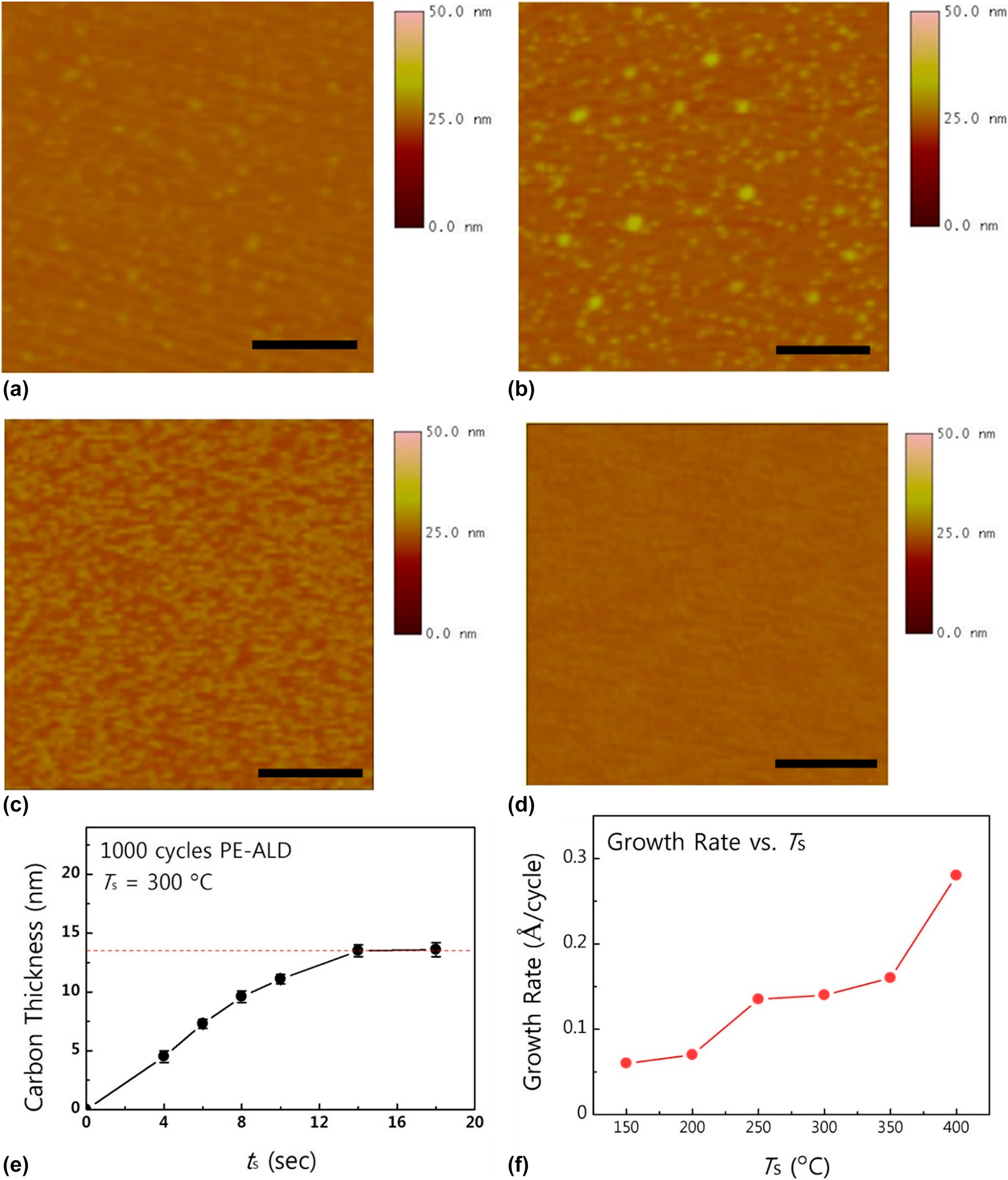
The growth characteristics of a-C were systemically investigated as a function of precursor exposure time and substrate temperature on a 2-step surface pretreated SiO2 substrate, as shown in Figs. 1(e) and 1(f). Unlike previous reports that a reliable ALD growth mode had not been achieved, ALD a-C using CBr4 shows growth saturation when the precursor exposure time is over 14 s, and the saturated growth rate of ALD a-C is 0.14 Å/cycle at 300 °C. The growth of ALD a-C shows a stable growth rate from 250 to 300 °C, and when the growth temperature exceeds 350 °C, CBr4 molecules start to dissociate into reactive CBrx (x < 4) because of the weak C–Br bonds [Reference Yamahata, Shigekawa, Kurishima and Matsuoka33, Reference Choi, Jung, Lee, Mun, Kim, Park and Kim34], losing its self-limiting growth nature. Since ALD ensures superior step coverage of thin films on a high aspect ratio structure owing to its peculiar growth mechanism, self-limiting growth of ALD a-C can be deposited inside via holes with excellent conformality (>90%).
In a Raman analysis of an ALD-grown a-C film, as shown in Fig. 2(a), every spectrum showed similar shape, regardless of the growth temperature. By deconvolution of the Raman spectrum of a-C grown at 300 °C, the mixed phase of nanocrystalline diamond (1650 cm−1), diamond (1340 cm−1), and disordered sp 3 carbon (1500 cm−1) was assigned to the deconvoluted Raman peaks, which corresponds to the well-known D, G, and D′ peaks, respectively. The presence of D, G, and D′ peaks in a single Raman spectrum of a-C indicates the ALD a-C film contains both nanocrystalline sp 3 and sp 2 graphitic carbon [Reference Chu and Li83]. X-ray photoelectron spectroscopy (XPS) was used to characterize an ALD-grown a-C film at 200 and 300 °C, as shown in Fig. 2(b). In deconvoluted C 1s spectra, various C peaks, including sp 2 graphitic carbon (284.6 eV), C–C (285.3 eV), C–O, or C–Br (286.1 eV), are observed regardless of the growth temperature. In the case of Br 3p spectra, two peaks at 183.2 and 190.1 eV are clearly observed when the growth temperature of a-C was 200 °C, but not at 300 °C. This indicates that an ALD a-C film grown at 200 °C contains some bromine residue, whereas the amount of bromine at 300 °C is negligible. In a quantitative analysis of the XPS spectra, a-C growth at 200 °C contains a significant amount of oxygen and bromine impurities in the film (approximately 17 and 2 at.%, respectively), whereas the a-C growth at 300 °C shows incorporation of less oxygen (approximately 9 at.%) with negligible bromine impurities. Since the reaction between CBr4 and atomic hydrogen is facilitated as the growth temperature increases, the remaining impurity (i.e., bromine) is much less when the growth temperature is 300 °C. Incorporation of a large amount of oxygen in the a-C growth at 200 °C might be originated from the ambient air, and the large portion of minor carbon species (e.g., C–C, C–O, or C=O) might have contributed to an increase in oxygen incorporation. In the Fourier-transform infrared (FT-IR) spectroscopy for measuring bonding characteristics of a-C [Fig. 2(c)], a couple of peaks indicating carbonaceous species are observed, which corresponds to sp 3 C–C stretching/C–H bending (1037 cm−1), sp 3 C–H/C–O stretching (1105–1375 cm−1), sp 2 C=C vibration (1614 cm−1), and C–Br stretching vibration (500–800 cm−1). In a microstructure analysis of an ALD a-C grown at 300 °C using transmission electron microscopy, as shown in Fig. 2(d), nano-graphitic fringes with intermixed sp 2 and sp 3 carbon lattices are observed, which matches the results from Raman spectroscopy. From these analyses of a-C, ALD a-C using CBr4 and H2 plasma can form high-quality a-C consisting of hydrogenated nanocrystalline sp 3 carbon and non-hydrogenated sp 2 carbon with incorporation of a small amount of oxygen and bromine.
(a) Raman and (b) XPS C 1s spectra of ALD a-C as a function of deposition temperature, and (c) FT-IR spectrum of ALD a-C grown at 300 °C. (d) HR-TEM image of a-C deposited on SiO2 substrate and Raman spectra of ALD a-C after (e) 1 min of diluted BOE etching (D.I. water:HF = 100:1) and (f) after O2 plasma as a function of ashing time. Reprinted from Ref. Reference Choi, Yeo, Song, Seo, Jang, Kim and Kim65 with permission from Elsevier.

The electrical properties of a-C were also characterized, and the possibility of using them for conformal conductive coating was investigated. The resistivity of ALD a-C grown at 200 and 300 °C, measured by the 4-point probe, was 1.62 and 0.25 Ω cm, respectively. In the same study, a bottom-gated transistor was fabricated, in which the channel is an a-C thin film grown at 200 and 300 °C, in order to further characterize the electrical properties. In the transfer curve, it can be seen that a-C shows weak p-type behavior regardless of the growth temperature. This p-type characteristic of a-C is generally observed in the other reports on diamond-like carbon or nanocrystalline graphitic carbon [Reference Robertson40, Reference Sagar, Zhang, Xiong and Yu84]. The calculated field-effect mobility of the 300 °C grown a-C transistor was 1.7 cm2/V s, whereas that of the transistor grown at 200 °C was 0.1 cm2/V s. The high resistivity and poor field-effect mobility of the a-C grown at 200 °C originated from the incorporation of a large amount of oxygen and bromine impurities, which deteriorate the electrical properties of a-C.
As mentioned in the introduction of this section, a-C is one of the essential materials for a multiple-patterning process, owing to its superior etch selectivity and ashability. These superior characteristics of ALD-grown a-C are proven by experiments. Figure 2(e) shows the Raman spectrum and the scanning electron microscopy image of an 18-nm-thick ALD a-C after buffered oxide etchant (BOE) etching on 100–500 nm SiO2 via hole substrate. After 1 min of BOE etching, the Raman spectrum remained unchanged, and the deposited a-C retained its structure when SiO2 was entirely etched by BOE, indicating a-C is resistant to HF. In addition, the deposited a-C was perfectly removed after 60 s of O2 reactive ion etching, as shown in Fig. 2(f). Both results demonstrated that ALD a-C using CBr4 precursor can be applied to the hard mask deposition for advanced multiple patterning, which requires a deposition technique that ensures high conformality.
In this section, the growth and film properties of a-C by ALD are discussed. Even though there is a lack of research on ALD-based a-C deposition to this day, conformal coating of a-C using ALD is considered a promising hard mask deposition technique for an advanced multiple-patterning process, which requires a coating technique with excellent step coverage, owing to its superior etch selectivity and ashability. Moreover, ALD-grown a-C shows good electrical properties and excellent conformality at a relatively low temperature compared to chemical vapor deposition (CVD), which can be applicable for various fields, such as conductive coating for 3D complex battery electrodes and corrosion resistive coating on electrochemical devices [Reference Dominko, Bele, Gaberscek, Remskar, Hanzel, Pejovnik and Jamnik85, Reference Scott, Jung, Cavanagh, Yan, Dillon, George and Lee86, Reference Zhu, Yang, Lv, Guo, Li, Zheng, Zhu and Yang87]. In particular, ALD-based a-C deposition on a lithium ion battery electrode is expected to be an effective coating that can help increase electrode conductivity, facilitate surface chemistry of active materials, and protect the electrode from direct contact with the electrolyte, leading to enhanced cycle life and ratio capability of batteries. Precise thickness control of carbon coating is essential in this case since a thick carbon coating layer would act as a barrier for Li+ diffusion, while a thin layer would hardly form a full coating layer on the surface of the substrate, leading to an increase in sheet resistance [Reference Dominko, Bele, Gaberscek, Remskar, Hanzel, Pejovnik and Jamnik85]. The application of ALD a-C coating can be extended to other materials having complex structures, which in turn enables an improvement of not only the process but also the performance of the devices.
Germanium oxide
In solid-state devices, Ge has been considered as a promising candidate for replacing Si, which can then overcome the current limitation of Si-based electronics. This is due to the high electron and hole mobility of Ge, making Ge-based electronics devices that operate at the high speed possible [Reference Goley and Hudait88, Reference Shin, Jiang, Ahn, Wu, Chung, Ye and Alam89, Reference Kamata90]. Despite these advantages of Ge, Ge-based electronics cannot be fabricated. One of the biggest problems of use of this material for device fabrication is its undesirable interfacial layer [Reference Goley and Hudait88]. When a high-k dielectric material is deposited on the Ge substrate by using ALD, the interfacial layer that is formed between the Ge and dielectric, caused by Ge diffusion, generates high defect densities that create electronic states in the bandgap, which deteriorate the device performance [Reference Goley and Hudait88]. To avoid this negative effect, numerous subsequent efforts to passivate interface defects have been made, including oxidation, nitridation, and chemical treatment [Reference Bodlaki, Yamamoto, Waldeck and Borguet91, Reference Xie, Deng, Schaekers, Lin, Caymax, Delabie, Qu, Jiang, Deduytsche and Detavernier92, Reference Oh, Kim, Lee, Song, Lee, Thompson, Lee, Kim, Maeng and Kim93]. Formation of GeO2 between the Ge substrate and high-k dielectric material has been also proposed to enhance the poor interfacial characteristics of Ge-based devices since this can suppress the formation of an unintended interlayer [Reference Kanematsu, Shibayama, Sakashita, Takeuchi, Nakatsuka and Zaima94].
Germanium oxides have diverse oxide phases, including GeO2, Ge2O3, GeO, and Ge2O [Reference Molle, Spiga and Fanciulli95]. Among these oxide phases, GeO and GeO2 are the two representative phases of germanium oxide, and stoichiometric GeO2 is known to be required for advanced Ge-based electronics, owing to its excellent electrical properties after formation [Reference Takagi, Maeda, Taoka, Nishizawa, Morita, Ikeda, Yamashita, Nishikawa, Kumagai, Nakane, Sugahara and Sugiyama96]. The formation of GeO, however, is inevitable during the gate dielectric deposition or post-deposition process because of the following reactions [Reference Kamata90]:
 $${\rm{Ge}}{{\rm{O}}_{\rm{2}}} + {\rm{Ge}} \to 2{\rm{Ge}}{{\rm{O}}_{\left( {\rm{s}} \right)}}\quad ,$$
 $${\rm{Ge}}{{\rm{O}}_{\left( {\rm{s}} \right)}} \to {\rm{Ge}}{{\rm{O}}_{\left( {\rm{g}} \right)}}\left( { > 400} \;{\rm{^\circ C}}\right)\quad {\rm{.}}$$
The formation of undesirable GeO deteriorates the device performance since GeO in the gas phase has high reactivity as a reducing agent [Reference Greenwood and Earnshaw97]. The reaction of gas-phase GeO with an adjacent device degrades the electrical properties of Ge-based electronics [Reference Kamata90]. To avoid this problem, deposition of GeO2 on a Ge substrate at a low process temperature has been proposed. There are various methods for forming GeO2, such as thermal and chemical oxidation, and vapor deposition [Reference Shibayama, Yoshida, Kato, Sakashita, Takeuchi, Taoka, Nakatsuka and Zaima98, Reference Bellenger, De Jaeger, Merckling, Houssa, Penaud, Nyns, Vrancken, Caymax, Meuris, Hoffmann, De Meyer and Heyns99, Reference Seo, Lee, Yoon, Park, Hwang, Kim, Yu and Cho100, Reference Busani, Plantier, Devine, Hernandez and Campidelli101, Reference Kita, Lee, Nishimura, Nagashio and Toriumi102, Reference Weis, Beckers, Wuttig, Lange and Njoroge103]. Thermal oxidation is one of the easiest ways to synthesize an oxide film on a Ge substrate. This method ensures uniform film growth on a 3D complex Ge structure. However, as mentioned, the undesirable GeO over 400 °C is inevitable during high-temperature annealing, resulting in deterioration of the Ge-based device properties. In addition, consumption of the Ge substrate (especially channel) may result in the deterioration of device performance, wherein the device consists of nanoscale thin films such as strain-Ge and Ge1−xSnx layers [Reference Kanematsu, Shibayama, Sakashita, Takeuchi, Nakatsuka and Zaima94]. Sputtering of GeO2 can deposit stoichiometric GeO2, but it does not satisfy the conformality and thickness controllability that modern devices require [Reference Kita, Lee, Nishimura, Nagashio and Toriumi102, Reference Weis, Beckers, Wuttig, Lange and Njoroge103, Reference Murphy, Grant, Sun, Jones, Jakubiak, Shutthanandan and Ramana104]. For these reasons, ALD has been considered as an excellent method to deposit high-quality GeO2 at low temperatures, especially when compared with other methods. However, since there has been a lack of precursors for GeO2 deposition to date, only a small number of reports on ALD GeO2 have been published [Reference Kanematsu, Shibayama, Sakashita, Takeuchi, Nakatsuka and Zaima94, Reference Perego, Scarel, Fanciulli, Fedushkin and Skatova105, Reference Jung, Kim, Shin and Kang106].
Perego et al. reported the deposition of GeO2 layer using the ALD process for fabrication of a Ge-based metal–oxide–semiconductor (MOS) capacitor [Reference Perego, Scarel, Fanciulli, Fedushkin and Skatova105]. In this article, even though a systematic analysis of the growth characteristics of ALD GeO2 is not presented, the ALD growth mode was observed using a divalent Ge precursor (1,2-bis((2,6-diisopropylphenyl)imino)acenaphthene germanium (dpp-BIAN)Ge) and an O3 reactant. The deposited germanium oxide showed stoichiometric GeO2 without any suboxide, and a negligible carbon impurity level. ALD-grown GeO2 also showed an amorphous phase with extremely smooth surface roughness [0.23 nm of root-mean-square (rms) roughness]. When the dielectric property was analyzed in the fabrication of a metal–insulator–semiconductor capacitor on a Ge substrate, the dielectric constant of the ALD-grown GeO2 was approximately 5.5, which is comparable to that of amorphous GeO2 [Reference Kar107]. The band structure of the GeO2/Ge heterojunction had been, on the other hand, investigated in order to understand the effect of a GeO2 layer on the high-k semiconductor band structure using XPS. The obtained bandgap of ALD GeO2 was approximately 5.81 eV, and the conduction band offset and valence band offset were 0.6 ± 0.1 and 4.5 ± 0.1 eV, respectively, which match with those from previous reports [Reference Ohta, Nakagawa, Murakami, Higashi and Miyazaki108]. According to the XPS measurement, ALD GeO2 using a divalent precursor was suggested to be a promising material for forming a passivation layer in a Ge-based device. The growth characteristics of ALD GeO2 were first reported in an experiment using two similar tetravalent precursors: bis(dimethylamino) (N,N′-diisopropyl-ethylenediamine)germanium and bis(dimethylamino) (N,N′-di-tert-butyl-ethylenediamine)germanium [Reference Jung, Kim, Shin and Kang106]. In this report, the self-limited growth behavior of ALD GeO2 was observed as a function of precursor pulse time for the two precursors. The ALD window from 200 to 320 °C was examined for the two precursors, and in both cases, the GeO2 film showed smooth surface roughness with negligible carbon impurities.
Only a small number of studies on ALD GeO2 have been published, and there is a lack of systematic studies on ALD GeO2, especially with regard to using a tetravalent precursor. Using a low-valent precursor might encourage ALD thin film growth at lower temperatures [Reference Dezelah IV, El-Kadri, Kukli, Arstila, Baird, Lu, Niinistö and Winter109]; however, it might also produce a film with different phases, including under-stoichiometric metal oxides [Reference Dezelah IV, El-Kadri, Szilágyi, Campbell, Arstila, Niinistö and Winter110]. For the purpose of forming a stoichiometric GeO2, a tetravalent Ge precursor could help form a stoichiometric GeO2 more favorably than using a divalent precursor. Yoon et al. recently reported a systematic study on ALD GeO2 using tetravalent precursors, tetrakis(dimethylamino)germanium (Ge(NMe2)4) and germanium n-butoxide (Ge(OnBu)4), and an O3 reactant [Reference Yoon, Oh, Lee, Song, Lee, Myoung, Kim, Moon, Shong, Lee and Kim111]. All the film properties of ALD GeO2 were compared with those of sputtered GeO2. Both precursors showed self-limited growth characteristics [Fig. 3(a)], in terms of saturated growth rate and increased linear thickness, as a function of precursor exposure time and the number of ALD cycles, respectively. The saturated growth rates of ALD GeO2 were 0.45 Å/cycle for Ge(NMe2)4 and 0.3 Å/cycle for Ge(OnBu)4 at 200 °C. It was noted that the exposure time of Ge(NMe2)4 for growth rate saturation is shorter than that of Ge(OnBu)4. From a density functional theory calculation, the reaction between surface hydroxyl and Ge(NMe2)4 was noted to be more thermodynamically favorable than the reaction between surface hydroxyl and Ge(OnBu)4, since the bond dissociation energies of O–Ge are much larger than that of N–Ge, resulting in a more stable bond formation [Reference Kachian, Wong and Bent112]. In addition, mobility of the molecules is inversely proportional to the molecular weight, thus the lighter Ge(NMe2)4 can be quickly attached on the substrate. Both the reactivity and mobility allow a short exposure time of Ge(NMe2)4 for surface saturation. The smaller growth rate of ALD GeO2 using Ge(OnBu)4 can be understood by the projected surface area of the adsorbed precursor species [Reference Park, Oh, Lee, Lee, Shin, Lansalot-Matras, Noh, Kim and Lee62]. In this case, the van der Waals radius of Ge(OnBu)3 (∼8.5 Å) is much larger than that of Ge(NMe2)4 (∼4.7 Å). Since the large size of the precursor hinders the reaction between the subsequent precursor and the surface hydroxyl species, the growth rate is, therefore, lowered. As shown in Fig. 3(b), the growth rate of ALD GeO2 using Ge(NMe2)4 increases rapidly when the growth temperature is over 250 °C, whereas the growth rate using Ge(OnBu)4 is retained from 200 to 330 °C. Because of the thermal decomposition of Ge(NMe2)4 with surface hydroxyl species, the growth rate increases rapidly, and a narrower range of process temperature can be observed than that using Ge(OnBu)4.
Growth rates of ALD GeO2 using Ge(NMe2)4 and Ge(OnBu)4 as a function of (a) precursor exposure time and (b) growth temperature, and deconvoluted XPS spectra of (c) Ge 3d and (d) O 1s. (e) Transmittance and (f) EDS line spectra of etched GeO2 films on transparent glass. Reprinted with permission from Ref. Reference Yoon, Oh, Lee, Song, Lee, Myoung, Kim, Moon, Shong, Lee and Kim111. Copyright 2018 American Chemical Society.

As mentioned in the introduction of this section, deposition of stoichiometric GeO2 is important for semiconductor applications. Stoichiometric GeO2 was deposited with Ge(NMe2)4 and Ge(OnBu)4 precursors. In the XPS measurement of ALD and sputtered germanium oxide films, the “O/Ge” ratio for ALD was approximately 1.96 for Ge(OnBu)4 and approximately 1.95 for Ge(NMe2)4, whereas that of sputtered was ∼1.87. This stoichiometry of ALD GeO2 was determined based on the presence of suboxide in the GeO2 film. From the XPS analysis, as shown in Figs. 3(c) and 3(d), Ge 3d and O 1s peaks of ALD and sputtered GeO2 can be deconvoluted to two peaks: one is the O–Ge–O (Ge4+) peak and the other is the O–Ge (Ge2+) peak. Among the various Ge suboxides, germanium monoxide is known to have negative components which degrade the electrical properties of GeOx by acting as trap sites and oxygen vacancies [Reference Oniki, Koumo, Iwazaki and Ueno113]. The presence of GeO in the GeO2 film leads to an increase in leakage of current; thus, it is highly important to suppress the formation of GeO while depositing GeO2. The thermally grown GeO2 at a process temperature of over 500 °C contains a considerable amount of GeO because GeO can be transformed from GeO2, as described in the introduction. That means GeO2 bond can be easily transformed to GeO by external energy. Similarly, highly energetic species such as ions or radicals might induce the formation of GeO, resulting in an undesirable stoichiometric of the GeO2 film grown by sputtering.
As described in the previous paragraph, the formation of GeO could be suppressed when the process temperature is sufficiently low. In other words, the presence of the suboxides in GeO2 can also be presumed by the etch properties of the GeO2 film in water since the wet etch rate of germanium oxide depends on its stoichiometry or crystallinity [Reference Kamata90]. Figure 3(e) shows the transmittance of 50-nm-thick GeO2 on a transparent glass substrate after 1 s of water etching. Unlike the transmittance spectra of ALD-grown GeO2, relatively poor transmittance was observed on sputtered GeO2. To quantify the residue after water etching of GeO2, energy-dispersive X-ray spectrometry was used for those samples after 1 s of water etching [Fig. 3(f)]. In this experiment, a negligible Ge signal was observed for ALD-grown GeO2 films, indicating that almost every GeO2 was dissolved in water, whereas over 5% of Ge remained for the sputtered GeO2 substrate. Even though the etch rates of GeO2 grown by ALD and sputtering were similar, germanium oxide phases other than GeO2 were not etched completely. Especially, amorphous GeO was insoluble, thus the undissolved phase of germanium oxide would remain as a noncontinuous morphology, deteriorating the transmittance of the GeO2 film.
From the microstructure analysis by X-ray diffraction (XRD), all the GeO2 films grown by ALD and sputtering show an amorphous phase. When the mass densities of the GeO2 film were measured by X-ray reflectivity (XRR), a relatively small density of sputtered GeO2 (2.08 g/cm3) was obtained when compared with that of ALD GeO2 based on Ge(NMe2)4 (2.24 g/cm3) or based on Ge(OnBu)4 (2.35 g/cm3). This is due to the incorporation of a large amount of GeO species in the sputtered GeO2 film. In the case of surface roughness measured by XRR, ALD-grown GeO2 films show smooth surface (rms roughness ∼0.38 nm), whereas sputtered GeO2 showed comparatively high roughness (approximately 2.80 nm). A similar trend on surface morphology of deposited GeO2 was also found on roughness measurement by atomic force microscopy (AFM). The rms roughness of ALD GeO2 by Ge(NMe2)4, Ge(OnBu)4, and sputtered GeO2 was 0.2, 0.1, and 2.9 nm, respectively. Owing to the peculiar growth characteristics of ALD, the ALD-grown GeO2 shows smooth surface compared with sputtered GeO2.
For the electrical property evaluation of ALD GeO2, an MOS capacitor was fabricated on the Si substrate. The thickness of ALD and sputtered GeO2 was fixed to 10 and 30 nm, respectively. The capacitance–voltage (C–V) and current–voltage (I–V) curves are presented in Figs. 4(a) and 4(b). The C–V curves of the ALD-grown GeO2 show typical behavior of dielectric materials on p-Si substrate with small hysteresis (∼100 mV) and interface state density (D it) (1.6 × 10¹² and 8.3 × 10¹¹ for ALD GeO2 by Ge(NMe2)4 and Ge(OnBu)4, respectively). The calculated dielectric constants of ALD GeO2 by Ge(NMe2)4 and Ge(OnBu)4 are 5.77 and 5.94, respectively, and these are well-matched with those that are previously reported for GeO2 films [Reference Murad, Baine, McNeill, Mitchell, Armstrong, Modreanu, Hughes and Chellappan114]. On the other hand, in the case of the C–V curve of sputtered GeO2, the accumulated capacitance is smaller than that of ALD GeO2 (k ∼ 1.05), and a large hysteresis (∼2 V) and D it (∼9.2 × 10¹²) are also observed. In an I–V analysis, the leakage current density of ALD GeO2 is acceptable for the dielectric [∼5.0 × 10⁻⁷ and 1.7 × 10⁻⁷ A/cm2 at −1 MV/cm for ALD GeO2 by Ge(NMe2)4 and Ge(OnBu)4, respectively], whereas sputtered GeO2 shows poor leakage characteristics that cannot be applied to dielectric applications (4.2 × 10⁻² A/cm2). These poor electrical properties of sputtered GeO2 originated from the formation of GeO. Germanium monoxide is known to have poor electrical properties since the Ge–O bonds act as trap sites and oxygen vacancies, leading to a high leakage current and poor C–V characteristics.
(a) C–V and (b) I–V curves of MOS capacitor with 10-nm-thick sputtered and ALD GeO2 films prepared using Ge(OnBu)4 and Ge(NMe2)4 with 10-nm-thick ALD SiO2. C–V curves of CTM (c) before and (d) after etching by a droplet of water at RT for 1 s. Reprinted with permission from Ref. Reference Yoon, Oh, Lee, Song, Lee, Myoung, Kim, Moon, Shong, Lee and Kim111. Copyright 2018 American Chemical Society.

By utilizing ALD GeO2 as a water-soluble material, ALD GeO2 can also be applicable to the fabrication of a secure memory device. It has been demonstrated that the charge-trapping memory (CTM) that is fabricated with ALD GeO2 as a sacrificial layer can be easily broken by simply dropping a water droplet on the device, which loses its memory property. For the fabrication of a secure memory device, 40-nm-thick ALD GeO2 was deposited between the SiNx/SiO2 layer and the top ruthenium electrode as a control gate oxide using Ge(OnBu)4. The device structure and the electrical properties of the CTM device before and after water etching are shown in Figs. 4(c) and 4(d). Under normal operation conditions, charges were stored inside the SiNx layer, which is an ideal behavior for memory devices. When a single droplet of water was dropped on the device, however, the electrical properties of the CTM device were degraded, leading to the device losing its electrical information entirely.
In this section, the recent progress of ALD GeO2 is summarized. It has been proven in the literature that ALD GeO2 has excellent film properties that can be applied to Ge-based electronics. ALD GeO2 using tetravalent precursors (Ge(NMe2)4 and Ge(OnBu)4) shows low impurity level, negligible incorporation of suboxides such as GeO, high density, and low surface roughness. From the electrical property analysis of the MOS capacitor with ALD GeO2, it has been found that excellent dielectric properties with a comparable dielectric constant with those grown by other methods, and low defect densities are obtained, which indicates that ALD GeO2 is a suitable material for the fabrication of Ge-based electronics. In addition, owing to the water-soluble characteristics of the stoichiometric GeO2 film, the material also shows the possibility for being used in the fabrication of destructive memory devices. Although the water-erasable device presented in this review is only a prototype of a future secure device, it is believed that fabrication of this device using newly developed ALD-based GeO2 can be further advanced and lead to large-scale manufacturing.
2-Dimensional transition metal dichalcogenides
After the introduction of graphene, a 2D honeycomb structure of carbons, by Novoselov et al. [Reference Novoselov, Geim, Morozov, Jiang, Zhang, Dubonos and Grigorieva115], many researchers predicted that graphene will be a breakthrough that can overcome the current limitation of Si-based electronics, due to its remarkable electron mobility of over 10,000 cm2/V s with just a few atomic-layer-thick flakes [Reference Bolotin116]. Despite its superior conductivity, graphene itself does not have a bandgap (E g); thus, it cannot be used as the channel material for transistors. Instead, 2D TMDCs were the focus among promising candidate materials for future electronics from early 2010. TMDC is a type of layered 2D material with van der Waals interactions and consists of metal cores and chalcogen elements [Reference Manzeli, Ovchinnikov, Pasquier, Yazyev and Kis117]. TMDCs have strong in-plane covalent bonding and weak out-of-plane van der Waals bonding, which are similar to graphene, and their film properties depend on the number of TMDC layers [Reference Chhowalla, Shin, Eda, Li, Loh and Zhang118, Reference Yeh, Jin, Zaki, Zhang, Liou, Sadowski, Al-Mahboob, Dadap, Herman, Sutter and Osgood119]. A notable difference between graphene and TMDCs is the presence of a bandgap (E g). Predominantly, many TMDCs (MX2: M = Mo, W, X = S, Se, Te) exhibit semiconducting characteristics with a finite bandgap in the range of 1–2 eV [Reference Li, Wu, Yin and Zhang120, Reference Mak, Lee, Hone, Shan and Heinz121, Reference Tan and Zhang122]; thus, they can act as channel materials for complementary metal oxide semiconductor (CMOS) devices and other electronics. In 2011, superior electrical properties of exfoliated MoS2 were reported for the first time in the fabrication of a field-effect transistor, showing an on/off current ratio of ∼108 and electron mobility of over 200 cm2/V s [Reference Radisavljevic, Radenovic, Brivio, Giacometti and Kis123]. In addition, 2D TMDCs have been highlighted as a promising material for optoelectronic devices since they are thermodynamically and chemically stable, and they show a broad range of wavelengths for light absorption with only a couple of nanometer-thick sheets [Reference Mak and Shan124, Reference Brar, Sherrott and Jariwala125]. Many TMDCs are predicted to show unexpected characteristics with just a couple of atomic thickness that conventional 3D materials do not have, by numerous experiments and first principle calculations [Reference Manzeli, Ovchinnikov, Pasquier, Yazyev and Kis117, Reference Mak and Shan124, Reference Kaasbjerg, Thygesen and Jacobsen126, Reference Ali, Xiong, Flynn, Tao, Gibson, Schoop, Liang, Haldolaarachchige, Hirschberger, Ong and Cava127, Reference Rice, Young, Zan, Bangert, Wolverson, Georgiou, Jalil and Novoselov128, Reference Xu, Yao, Xiao and Heinz129]; thus, TMDCs have been considered a prospective material that can replace Si-based materials for electronics.
Despite the numerous advantages discussed, these materials have not been applied to mass production because of immature synthetic methods. Most of the early TMDC research focused on exfoliation from the bulk crystal because there was a lack of synthetic methods but exfoliation [Reference Radisavljevic, Radenovic, Brivio, Giacometti and Kis123, Reference Eda, Yamaguchi, Voiry, Fujita, Chen and Chhowalla130]. Physical and chemical exfoliation of TMDCs are simple methods for fabricating TMDC-based devices, since the flakes that are peeled off from the bulk crystal retain the original crystal structure, which allows maintenance of the superior electrical properties of the inherent material [Reference Kolobov and Tominaga131]. This method, however, only allows fabrication of laboratory-scale devices due to its poor transfer yield from bulk TMDC crystals. The number of TMDC layers is also hard to control by exfoliation; that is, the various characteristics of TMDCs that are determined by the number of layers cannot be modulated as intended. Thus, it is highly desirable to synthesize 2D TMDCs with large-area uniformity and layer controllability, with methods such as solution synthesis, chalcogenization of metal oxide, and direct CVD growth [Reference Kolobov and Tominaga131, Reference Sun, Li, Guo, Zhao, Fan, Dong, Xu, Deng and Fu132]. The direct CVD growth method is one of the fascinating methods for large-scale fabrication, which satisfies the requirement of large-area uniformity. By simultaneous exposure of metals and chalcogen precursors, TMDCs of 1–3 layers are formed on the substrate. Initially, the reacting chemical species start to form a TMDC flake with a triangular shape [Reference Najmaei, Liu, Zhou, Zou, Shi, Lei, Yakobson, Idrobo, Ajayan and Lou133], and it continues to grow when two or more MoS2 flake boundaries meet. Despite this facile way for MoS2 synthesis, a much improved wafer-scale uniformity and precise layer controllability by CVD are still challenging for large-scale device fabrication. In addition, the characteristics of TMDCs are poorer than those of mechanically exfoliated TMDCs because of the numerous grain boundaries that are generated during synthesis [Reference Manzeli, Ovchinnikov, Pasquier, Yazyev and Kis117]. In terms of these requirements, ALD is a promising method for 2D TMDC synthesis, since it can overcome these limitations owing to its peculiar deposition mechanism.
Synthesis of 2D TMDCs (WS2 and MoS2) by sulfurization of ALD-grown metal oxides
The initial research on ALD-based TMDC growth began with the chalcogenization of metal oxide that was deposited by ALD. In 2013, Song et al. reported WS2 nanosheet synthesis by sulfurization of ALD-grown WO3 [Reference Song, Park, Lee, Choi, Jung, Lee, Hwang, Myoung, Jung, Kim, Lansalot-Matras and Kim134]. WS2 is one of the TMDCs that has been widely studied owing to its peculiar characteristics, including electrical [Reference Ovchinnikov, Allain, Huang, Dumcenco and Kis135, Reference Chernikov, Van Der Zande, Hill, Rigosi, Velauthapillai, Hone and Heinz136], optical [Reference Kim, Kim, Lee, Lee, Choi, Lee, Lee, Jhang, Park, Cheong, Lee and Chung137, Reference Cong, Shang, Wang and Yu138, Reference Kajino, Oto and Yamada139], magnetic [Reference Plechinger, Nagler, Arora, Granados Del Águila, Ballottin, Frank, Steinleitner, Gmitra, Fabian, Christianen, Bratschitsch, Schüller and Korn140, Reference Ma, Dai, Guo, Niu, Lu and Huang141], and even catalytic properties [Reference Duan, Chen, Chambers, Andersson and Qiao142, Reference Lukowski, Daniel, English, Meng, Forticaux, Hamers and Jin143]. Despite these notable properties, there has been a lack of research on the synthesis of WS2 with excellent thickness controllability and large-area uniformity. In terms of layer controllability, however, sulfurization of ALD-grown oxide can easily overcome the limitations by controlling the thickness of the metal oxide before sulfurization. For the deposition of WO3, bis(isopropylcyclopentadienyl)tungsten(IV) dihydride (WH2(iPrCp)2) was used as a W precursor and O2 plasma as a reactant. Sulfurization of a WO3 film into WS2 nanosheets was conducted with S powder at 1000 °C for 30 min. The number of WS2 layers was easily controlled from monolayer to multilayers by changing the thickness of ALD-grown WO3. ALD WO3 films, grown over 20, 30, and 50 ALD cycles, were sulfurized at 1000 °C for 30 min, and those films were entirely transformed to nanosheets of 1, 1.6, and 3 nm, respectively, which correspond to the mono-, bi-, and tetra-layer of WS2 [Figs. 5(a)–5(c)]. The number of layers is estimated by the spacing between WS2 layers or the WS2 and SiO2 substrate. The spacing between WS2 and SiO2 is typically known to be 1 nm, and between WS2 layers is 0.6 nm, which are in good agreement with the estimated number of layers of sulfurized WS2 [Reference Gutiérrez, Perea-López, Elías, Berkdemir, Wang, Lv, López-Urías, Crespi, Terrones and Terrones144].
AFM images and height profiles (inset) of the transferred WS2 nanosheet on the SiO2 substrate for the (a) mono-, (b) bi-, and (c) tetra-layered thicknesses, respectively. (d) Raman spectra for the mono-, bi-, tetra-layer WS2 nanosheets on SiO2, and (e) relative Raman peak intensities and peak distances of the E12g and A1g bands for the WS2 layers. (f) PL spectra for the WS2 nanosheets. (g) HRTEM image of the monolayer WS2 nanosheet, and (h) large area uniformity (approximately 13 cm) of WS2 nanosheet on SiO2 substrate. (i) HRTEM image of the tetra-layer WNT and (inset) the intensity profile of the region denoted by the solid line. (j) Electrical properties of the monolayer WS2 nanosheet by fabrication of FET. Reprinted with permission from Ref. Reference Song, Park, Lee, Choi, Jung, Lee, Hwang, Myoung, Jung, Kim, Lansalot-Matras and Kim134. Copyright 2013 American Chemical Society.

Raman spectroscopy and photoluminescence (PL) that are shown in Figs. 5(d)–5(f) were used to distinguish the number of WS2 layers. In Raman spectroscopy, two clear peaks from in-plane and out-of-plane vibration of WS2 were observed at approximately 356 and 420 cm−1 for mono-, bi-, and tetra-layers of WS2. As the number of WS2 layers increases, two notable changes can be observed, which are the peak intensity ratio of E12g and A1g, and the peak distance between them, as shown in Fig. 5(e). As the number of WS2 layers increases from mono- to tetra-layer, the peak intensity ratio increases because the Raman intensity is mainly affected by the scattering volume of WS2 [Reference Berkdemir, Gutiérrez, Botello-Méndez, Perea-López, Elías, Chia, Wang, Crespi, López-Urías, Charlier, Terrones and Terrones145]. The peak distance between E12g and A1g also increases as the number of WS2 layers increases, owing to the weak interlayer interaction and reduced long-range Coulomb interaction between the effective charges in WS2 layers that originated by an increase in the dielectric screening [Reference Najmaei, Liu, Zhou, Zou, Shi, Lei, Yakobson, Idrobo, Ajayan and Lou133, Reference Molina-Sánchez and Wirtz146]. From a PL analysis, as shown in Fig. 5(d), a strong signal of monolayer WS2 can be observed at 2.01 eV, which corresponds to the reported E g of the WS2 monolayer. However, only weak signals can be observed at 1.97 eV for bilayer WS2, and 1.4 eV for the tetra-layer. This phenomenon is originated by direct to indirect E g transition of 2D TMDCs, which closely matched with previous reports [Reference Mak, Lee, Hone, Shan and Heinz121, Reference Gutiérrez, Perea-López, Elías, Berkdemir, Wang, Lv, López-Urías, Crespi, Terrones and Terrones144]. The stoichiometry of the WS2 layer was confirmed by quantitative analysis using XPS, in which the calculated ratio of W and S was 2, indicating that sulfurization of WO3 at 1000 °C can form a stoichiometric WS2 [Reference Lee, Yu, Wang, Fang, Ling, Shi, Te Lin, Huang, Chang, Chang, Dresselhaus, Palacios, Li and Kong147]. In high-resolution transmission electron microscopy (HRTEM) analysis, the WS2 nanosheet that was transferred onto the TEM grid shows periodically arranged atoms, and the selected area electron diffraction (SAED) pattern [as shown in the inset of Fig. 5(g)] also shows the polycrystalline (100) and (110) phase of WS2, in which the grain size is approximately 10–20 nm. The grain size of WS2 is comparable to that of the MoS2 nanosheet synthesized by Mo sulfurization [Reference Zhan, Liu, Najmaei, Ajayan and Lou148].
ALD-based TMDC synthesis satisfies the requirements of large-area uniformity and excellent conformality for film deposition. These requirements are prerequisites for large-scale device fabrication, owing to the peculiar growth characteristics and self-limiting growth manner that can be expected from satisfying these requirements. ALD-based WS2 synthesis also showed wafer-scale uniformity up to 6 inches [Fig. 5(h)]. In addition, in terms of excellent conformality of ALD, WS2 nanotubes were well synthesized by forming WS2 on SiO2/Si nanowire, followed by etching with HF [Fig. 5(i)]. By using ALD-based WS2 synthesis, not only the number of WS2 layers but also the diameter or even the length of the nanotube can be modulated, which cannot be achieved by other methods. From the electrical property characterization of ALD-based WS2 by fabrication of a field-effect transistor (FET) [Fig. 5(j) for the transfer curve of monolayer WS2-FET], the electron mobility and sub-threshold swing (SS) were 3.9 cm2/V s and 0.6 V/dec, respectively. In particular, the electron mobility was much higher than that of WS2 FETs that had been previously reported due to the suppression of charged impurity scattering by deposition of high-k dielectric, also known as the dielectric screening effect [Reference Radisavljevic, Radenovic, Brivio, Giacometti and Kis123, Reference Chen, Xia, Ferry and Tao149, Reference Jena and Konar150].
MoS2, one of the well-known 2D TMDCs owing to its superior electrical and optical properties [Reference Radisavljevic, Radenovic, Brivio, Giacometti and Kis123, Reference Lembke and Kis151, Reference Zongyou, Hai, Hong, Lin, Yumeng, Yinghui, Gang, Qing, Xiaodong and Hua152], was also synthesized using the chalcogenization method. In 2015, Song et al. reported a synthetic method for MoS2 using sulfurization of ALD-grown MoOx [Reference Song, Ryu, Lee, Sim, Lee, Choi, Jung, Kim, Lee, Myoung, Dussarrat, Lansalot-Matras, Park, Choi and Kim153]. In this report, MoOx was grown on a SiO2/Si substrate using Mo(CO)6 as a precursor and O2 plasma as a reactant at 200 °C. As shown in Fig. 6(a), the MoS2 that was synthesized using one-step sulfurization, which was also previously used for WS2 synthesis [Reference Song, Park, Lee, Choi, Jung, Lee, Hwang, Myoung, Jung, Kim, Lansalot-Matras and Kim134], showed numerous granular-like particles on top of the surface, which was formed by the vaporization of MoOx that occurred at approximately 700 °C [Reference Blackburn, Hoch and Johnston154]. Since this rough surface was not suitable for smooth TMDC synthesis, two-step sulfurization was applied to avoid the vaporization of ALD MoOx. For two-step sulfurization, ALD MoOx was initially sulfurized at 600 °C for 60 min, which can avoid the vaporization of MoOx, and the process temperature was then increased to 1000 °C and maintained for 30 min. MoS2 that was synthesized using two-step sulfurization shows a smooth surface, compared with that of MoS2 that is synthesized by one-step sulfurization. Similarly, Keller reported the synthesis of MoS2 by sulfurization of an ALD-grown MoOx film using a bis(tert-butylimido)bis(dimethylamido)molybdenum [(tBuN)2(NMe2)2Mo] precursor [Reference Keller, Bertuch, Provine, Sundaram, Ferralis and Grossman155], and a similar granular-like nucleation was observed after the sulfurization of MoOx. In this article, the granular nature of the synthesized MoS2 was caused by the morphology of precursor oxide formed and could be solved through pretreatment methods, such as piranha cleaning, to increase the density of surface hydroxyl, resulting in a smooth growth of precursor oxide on the substrate. The number of MoS2 layers was controlled by changing the thickness of the MoOx, as shown in Fig. 6(b). In this experiment, 6, 9, and 12 cycles of ALD MoOx were entirely transformed to 1, 1.6, and 2.3 nm of MoS2, which correspond to the mono-, bi-, and tri-layer of MoS2, respectively [Reference Chhowalla, Shin, Eda, Li, Loh and Zhang118, Reference Eda, Yamaguchi, Voiry, Fujita, Chen and Chhowalla130]. Raman and PL spectra of MoS2 grown using ALD MoOx showed that the Raman peak distance between E12g and A1g increased as the number of layers increases and the strong PL peak for the monolayer MoS2 disappeared when the number of MoS2 layers increased. These patterns are the same as those observed for WS2, as described in the previous paragraph.
(a) AFM images of sulfurized MoOx thin film using one-step sulfurization at 1000 °C and two-step sulfurization at first-sulfurization temperature of 600 °C. (b) Height profiles of transferred MoS2 on SiO2 substrate for mono-, bi-, and trilayer thickness. (c) Raman and PL spectra, and (d) HR-TEM image of MoS2 and (inset) FFT pattern [Reference Song, Ryu, Lee, Sim, Lee, Choi, Jung, Kim, Lee, Myoung, Dussarrat, Lansalot-Matras, Park, Choi and Kim153].
Synthesis of Mo1−xWxS2 by sulfurization of ALD-grown Mo1−xWxOy
The focus of bandgap modulation of 2D TMDCs was mainly on the performance enhancement of optoelectronic devices, such as photodiode or phototransistor [Reference Bernardi, Palummo and Grossman156, Reference Wang, Kalantar-Zadeh, Kis, Coleman and Strano157], because of its superior light absorption characteristics in a couple of nanometer-thick TMDC sheets. Even though the E g of TMDCs can be modulated by changing the number of layers, alloying two different TMDCs with different E g can tune the E g of TMDCs with great flexibility and access an almost continuous light absorption range [Reference Kutana, Penev and Yakobson158, Reference Susarla, Kutana, Hachtel, Kochat, Apte, Vajtai, Idrobo, Yakobson, Tiwary and Ajayan159]. One of the notable differences of ALD among various deposition methods is that ALD enables a precise control of composition of the film by intermixing two different ALD processes in a single ALD step. This method is called supercycle and is frequently used for doping or alloy ratio control of ternary or quaternary compounds [Reference Nam, Lee, Cheon, Lee, Kim, Kwon, Lee and Kim18, Reference Nam, Lee, Kim and Kim22, Reference Bakke, Tanskanen, Jung, Sinclair and Bent160, Reference Banerjee, Lee, Bae, Lee and Rubloff161, Reference Adelmann, Tielens, Dewulf, Hardy, Pierreux, Swerts, Rosseel, Shi, Van Bael, Kittl and Van Elshocht162, Reference Thimsen, Riha, Baryshev, Martinson, Elam and Pellin163, Reference Ahvenniemi, Matvejeff and Karppinen164]. Hence, alloys of 2D TMDCs can be formed by sulfurization of alloyed metal oxides in which composition is precisely controlled by the ALD supercycle.
Based on the synthesis of MoS2 and WS2 that are introduced in the section “Synthesis of 2D TMDCs (WS2, MoS2) by sulfurization of ALD-grown metal oxides,” Mo1−xWxS2 alloys were synthesized by sulfurization of Mo1−xWxOy alloy grown by an ALD supercycle [Reference Song, Ryu, Lee, Sim, Lee, Choi, Jung, Kim, Lee, Myoung, Dussarrat, Lansalot-Matras, Park, Choi and Kim153]. The composition of Mo1−xWxOy was easily controlled by changing the number of ALD cycles in a single ALD supercycle, and systematic modulation of Mo1−xWxS2 composition was confirmed by XPS quantification analysis. As shown in Fig. 7(a), synthesized Mo1−xWxS2 alloys that were sulfurized by a single supercycle of Mo1−xWxOy show 1 nm of thickness regardless of the alloy ratio, which is the thickness of a single layer of Mo1−xWxS2. That is, two or more layers of Mo1−xWxS2 can be synthesized by increasing the number of Mo1−xWxOy supercycle, allowing excellent layer controllability of Mo1−xWxS2. The intermix of Mo1−xWxS2 was confirmed by Raman spectroscopy, PL, and XPS analysis. In particular, the notable shift of PL peaks intended was observed, which was depending on their composition ratios. As shown in Figs. 7(b) and 7(c), the peak position of the Mo1−xWxS2 alloy from the PL spectra shows generally a gradual increase in the PL peak position as the amount of W in the alloy increases, except for the Mo0.7W0.3S2 sample, which is due to the bowing effect that has been observed in many semiconductor alloys [Reference Yin, Gong and Wei165, Reference Chen, Xi, Dumcenco, Liu, Suenaga, Wang, Shuai, Huang and Xie166].
(a) Height profiles of transferred Mo1−xWxS2 alloys on SiO2 substrate. (b) PL spectra of monolayer Mo1−xWxS2 alloys and (c) the PL peak position versus W composition. (d) Calculated atomic concentration of Mo1−xWxS2 from ARXPS as a function of emission angle, and (e) calculated Raman peak distances between A1g and E12g from Mo1−xWxS2 alloys [Reference Song, Ryu, Lee, Sim, Lee, Choi, Jung, Kim, Lee, Myoung, Dussarrat, Lansalot-Matras, Park, Choi and Kim153].

Vertically composition-controlled (VCC) Mo1−xWxS2, which has been highlighted in high-performance optoelectronics owing to its interlayer functionality, such as interlayer transition, was also synthesized by sulfurization of a VCC Mo1−xWxOy film [Reference Hong, Kim, Shi, Zhang, Jin, Sun, Tongay, Wu, Zhang and Wang167, Reference Koåmider and Fernández-Rossier168]. Prior to sulfurization, the VCC Mo1−xWxOy film was deposited with 5 ALD supercycles at different ALD cycle ratios. Initially, 20 cycles of ALD WO3 were conducted on a SiO2 substrate, which correspond to growing a monolayer of WS2. Three supercycles with different ALD cycle ratios were sequentially conducted, from WO3-rich to MoOx-rich alloys. Each supercycle with a different ALD cycle ratio was consistent with a monolayer of Mo1−xWxS2 alloy. Finally, 3 cycles of ALD MoOx, which correspond to a MoS2 monolayer, were conducted. After sulfurization of VCC Mo1−xWxOy, AFM measurement of VCC Mo1−xWxS2 confirmed that 5 layers of the TMDC alloy were synthesized by sulfurization of 5 sequential ALD supercycles (approximately 3.5 nm). Moreover, angle-resolved XPS (ARXPS) and Raman peak distance results [as shown in Figs. 7(d) and 7(e)] showed that atomic concentration of VCC Mo1−xWxS2 was gradually changed from the lowermost layer to the uppermost layer, demonstrating the synthesis of Mo1−xWxS2 alloy with controlled composition based on the ALD process.
With this VCC Mo1−xWxS2 method, not only the composition controllability but also an additional effect from interlayer couplings, for instance, interlayer transitions, can be obtained [Reference Tongay, Fan, Kang, Park, Koldemir, Suh, Narang, Liu, Ji, Li, Sinclair and Wu169, Reference Yu, Hu, Su, Huang, Liu, Jin, Purezky, Geohegan, Kim, Zhang and Cao170]. Compared with the VCC Mo1−xWxS2 that were stacked by the transfer method of each differently composed Mo1−xWxS2 alloy, greater light absorption was obtained for VCC Mo1−xWxS2 synthesized by sulfurization of Mo1−xWxOy with ultraviolet-visible (UV-Vis) spectroscopy, owing to its strong interlayer coupling that cannot be obtained by other methods. When the light absorption spectrum of VCC Mo1−xWxS2 that are stacked was subtracted from that of VCC Mo1−xWxS2 synthesized by sulfurization, a small absorbance peak was observed at 1.87 eV, which was formed by a strong interlayer coupling. In addition, the incorporation of contaminants, including H2O or organic compounds, can be avoided by using this ALD-based VCC Mo1−xWxS2 synthesis [Reference Gong, Lin, Wang, Shi, Lei, Lin, Zou, Ye, Vajtai, Yakobson, Terrones, Terrones, Tay, Lou, Pantelides, Liu, Zhou and Ajayan171]. Since the VCC Mo1−xWxS2 exhibited superior light absorption in a wide range of wavelengths, as well as strong interlayer coupling, 5 layers of VCC Mo1−xWxS2 alloy were utilized as the active layer of the photodetector. Compared with photodetectors that were fabricated with 5 layers of MoS2 or WS2, the VCC Mo1−xWxS2–based photodetector generated a broadband of photo-induced current from 1.2 to 2.5 eV, whereas MoS2− or WS2-based photodetectors generated a narrower photocurrent, from 1.3 to 2.1 eV for the WS2 photodetector and from 1.2 to 1.8 eV for the MoS2 photodetector. Furthermore, when white light was applied to the photodetectors, the Mo1−xWxS2–based photodetector showed 3 and 4 times higher photocurrent than those of WS2 and MoS2, respectively, which was attributed to broadband light absorption of VCC Mo1−xWxS2. These results demonstrated that VCC Mo1−xWxS2 is a promising material for advanced optoelectronic applications.
Direct synthesis of 2D TMDCs by ALD
Even though the sulfurization of ALD-grown metal oxides using ALD is advantageous, this two-step process requires an additional sulfurization process as compared to the direct ALD process, which can be used to synthesize TMDCs with one step. The complexity of the process leads to an increase in cost, and sulfurization results in poor crystalline quality and small domain size, which may deteriorate the electrical properties of TMDCs [Reference Lin, Zhao, Zhou, Zhong, Wang, Tsang and Chai172]. Hence, it is highly desirable to synthesize TMDCs with the direct ALD process. In 2014, L. Tan reported a direct synthesis of ALD MoS2 at 300 °C using MoCl5 and H2S as a precursor and reactant, respectively [Reference Tan, Liu, Teng, Guo, Low and Loh173]. AFM and TEM analyses confirmed the exact thickness controllability of MoS2, which indicated that conventional ALD growth of MoS2 was obtained. Moreover, the crystallinity of MoS2 was increased by using post-deposition annealing with sulfur vapor at 800 °C, which led to the recrystallization of MoS2 at high annealing temperature. Furthermore, Jurca et al. reported a low-temperature growth of ALD MoS2 using a metal–organic precursor, tetrakis(dimethylamido)molybdenum [Reference Jurca, Moody, Henning, Emery, Wang, Tan, Lohr, Lauhon and Marks174]. In contrast to a halide precursor, the metal–organic precursor enabled the low-temperature growth of ALD TMDC owing to its high reactivity with oxidants. Moreover, the use of the metal–organic precursor prevented a deleterious effect of by-products that could be generated after the reaction between a halide precursor and a reactant (e.g., HCl). Similarly previous reports described the conventional ALD growth of MoS2 [Reference Nandi, Sahoo, Sinha, Yeo, Kim, Bulakhe, Heo, Shim and Kim175, Reference Mattinen, Hatanpää, Sarnet, Mizohata, Meinander, King, Khriachtchev, Räisänen, Ritala and Leskelä176, Reference Pyeon, Kim, Jeong, Baek, Kang, Kim and Kim177, Reference Jin, Shin, Kwon, Han and Min178]; however, when the process temperature was sufficiently high, the growth mechanism of direct ALD TMDCs was significantly altered. In 2016, Kim et al. reported direct ALD synthesis of MoS2 and WSe2 using MoCl5 and WCl6 as precursors, and H2S and diethyl selenide (DESe) as reactants [Reference Kim, Song, Park, Ryu, Lee, Kim, Jeon, Lee, Woo, Choi, Jung, Lee, Myoung, Im, Lee, Ahn, Park and Kim179, Reference Park, Kim, Song, Kim, Wanlee, Ryu, Lee, Park and Kim180]. A notable feature of direct ALD synthesis of TMDCs using these precursors at over 500 °C is that the number of TMDC layers is determined by process temperature, not the number of ALD cycles. As shown in Figs. 8(a) and 8(b), the peak distance between A1g and E12g of ALD-synthesized MoS2, and also the thickness of WSe2, are saturated even when the number of ALD cycles increases, which indicates that this sequential exposure of the precursor and reactants does not show a conventional ALD growth manner. Instead, a thicker TMDC layer was obtained at a lower temperature for the synthesis of both TMDCs. For instance, as shown in Fig. 8(c), tri-layer MoS2 (approximately 2 nm) was synthesized when the process temperature was 500 °C, while the process temperature increased to 700 and 900 °C, bi- (approximately 1.4 nm) and mono-layer MoS2 (approximately 0.8 nm) were obtained. This peculiar phenomenon, known as the “self-limiting layer synthesis” (SLS), is considered to be caused by the inherent chemical inactivity of the TMDCs’ surface [Reference McDonnell, Brennan, Azcatl, Lu, Dong, Buie, Kim, Hinkle, Kim and Wallace181]. When the first layer of ALD TMDC is formed on the substrate, there is a lack of precursor chemisorption site on the initially formed TMDC layer because of its chemical inactivity [Reference McDonnell and Wallace182]. Only a physisorbed precursor on the TMDC layers could react with subsequent reactants. However, when the process temperature is high enough, the physisorbed chemical species are easily detached from the TMDC layer; thus, the synthesis of a TMDC layer as a function of ALD cycle is hindered [Reference McDonnell, Brennan, Azcatl, Lu, Dong, Buie, Kim, Hinkle, Kim and Wallace181]. Furthermore, the surface potential that was induced by the positive charge between MoS2 and SiO2 substrates helps to adhere the precursor on the MoS2 substrate physically, and this potential would decrease when the number of layers increases, which would then increase the distance between the physisorbed precursor molecule and the interfacial charge [Reference Castellanos-Gomez, Cappelluti, Roldán, Agraït, Guinea and Rubio-Bollinger183]. It has been observed that the peak distance increased between E12g and A1g when the Raman analysis and PL signal intensity decreased in a SLS-grown MoS2, which occurred as the number of layers increased. This is similar to the pattern observed in sulfurized MoS2, as discussed in the previous section. The intensity ratio of E12g and A1g of WSe2 obtained from Raman analysis also decreased when the number of layers increased.
(a) Raman peak distance of MoS2 and (b) thickness of WSe2 measured by AFM as a function of process temperature. (c) AFM images of MoS2 and WSe2 depending on the process temperature and large-area uniformity of MoS2 and WS2 [Reference Kim, Song, Park, Ryu, Lee, Kim, Jeon, Lee, Woo, Choi, Jung, Lee, Myoung, Im, Lee, Ahn, Park and Kim179]. Reprinted with permission from Ref. Reference Park, Kim, Song, Kim, Wanlee, Ryu, Lee, Park and Kim180. Copyright 2016 IOP Publishing.

Both MoS2 and WSe2 grown by the SLS method showed wafer-scale large-area uniformity up to 1.5 × 8 cm2, as shown in Fig. 8(c), in which the size is limited by the reactor design. In the TEM analysis, SLS-grown monolayer MoS2 and tri-layer WSe2 showed excellent layer uniformity of over 95 and 90%, respectively, and both TMDCs have (100) and (110) planes of crystallinity. The electrical properties of monolayer SLS-grown MoS2 were characterized by FET fabrication and showed n-type behavior with 0.2 cm2/V s of field-effect electron mobility in the linear regime, 108 of on/off current ratio, and 0.36 V/dec of SS, which are comparable to those of single-crystal MoS2 [Reference Radisavljevic, Radenovic, Brivio, Giacometti and Kis123, Reference Castellanos-Gomez, Cappelluti, Roldán, Agraït, Guinea and Rubio-Bollinger183]. In the case of tri-layer SLS-grown WSe2, the material exhibited p-type characteristics with 2.2 cm2/V s of field-effect hole mobility and 106 of on/off current ratio, which are significantly higher than those previously reported for WSe2 grown with the CVD method [Reference Huang, Yang, Liu, Chen, Fu, Xiong, Lin and Xiang184].
Since the MoS2 growth using the MoCl5 precursor depends critically on the underlying substrate due to physisorption of the precursor, this SLS method can be applied to the synthesis of heterostructure of 2D TMDCs with precise layer controllability, which is challenging for conventional methods [Reference Dong and Kuljanishvili185]. The MoS2/WSe2 heterostructure was fabricated by synthesizing SLS-grown MoS2 at 800 °C on the exfoliated WSe2 flakes on a SiO2/Si substrate. In the Raman spectra shown in Fig. 9(a), MoS2-related peaks (E12g and A1g) are observed only on the SiO2 and bilayer WSe2, not on the 12-layer WSe2, which indicates the monolayer MoS2 was only formed on the SiO2 and bilayer WSe2, not on the 12-layer WSe2. This was also confirmed from the Raman mapping for MoS2 E12g peak intensity and position, shown in Fig. 9(b). In the mapping images, the MoS2-related peak is only observed on the bare SiO2 and 2 L of WSe2, not on the bulky WSe2 layers. As discussed, the synthesis of SLS-grown MoS2 was inhibited on the 12-layer WSe2 because of the lack of force for the precursor molecules to physisorb on top of the WSe2 layer. In addition, there was no intermixing of MoS2 and WSe2 during the synthesis, as evidenced by the fact that no Raman peak related to MoSe2 or WSe2 was observed. Using this method for heterostructure fabrication, which enables precise layer control of MoS2 on 2D TMDCs, a high-performance PN diode was also fabricated [optical microscopy image of the PN diode is shown in Fig. 9(c)]. The diode showed gate-tunable rectifying characteristics, which was explained by the variation in carrier density with electrical doping [Reference Furchi, Pospischil, Libisch, Burgdörfer and Mueller186]. From the PL spectra, the PN diode exhibited a strong PL quenching and photovoltaic effect because of a rapid carrier separation at the junction of MoS2/WSe2 [Reference Lee, Lee, Van Der Zande, Chen, Li, Han, Cui, Arefe, Nuckolls, Heinz, Guo, Hone and Kim187, Reference Fang, Battaglia, Carraro, Nemsak, Ozdol, Kang, Bechtel, Desai, Kronast, Unal, Conti, Conlon, Palsson, Martin, Minor, Fadley, Yablonovitch, Maboudian and Javey188]. As shown in Figs. 9(d) and 9(e), the I–V characteristics of the MoS2/WSe2 PN diode at gate voltage (V g) = −50 V showed an excellent photoresponsivity of 33 mA/W at drain-source voltage (V ds) = 1 V with an open circuit voltage (V oc) of 0.2 V.
(a) Raman spectra of SLS MoS2 on SiO2, bilayer WSe2, and 12-layer WSe2, and (b) optical microscope image and Raman mapping for MoS2 E12g peak intensity and position. (c) Optical microscope image of a MoS2/WSe2 heterostructure PN diode, and (d) I–V characteristics of the PN diode with various gate biases (inset: forward/reverse current ratio at V ds = |5 V|), and (e) with and without light illumination, and calculated photoresponsivity [Reference Kim, Song, Park, Ryu, Lee, Kim, Jeon, Lee, Woo, Choi, Jung, Lee, Myoung, Im, Lee, Ahn, Park and Kim179].

However, as mentioned in the first part of this chapter, not every synthesis of TMDCs using ALD shows SLS behavior, which depends on the process temperature. Recently, Kim et al. reported a conventional ALD growth of MoS2 using MoF6 and H2S [Reference Kim, Choi, Woo, Lee, Ryu, Lim, Lee, Lee, Im, Ahn, Kim, Park and Kim189]. Unlike the synthesis of MoS2 using MoCl5, the number of MoS2 layer synthesized by using the MoF6 precursor was linearly increased with the number of ALD cycles. As shown in Figs. 10(a) and 10(b), the thickness of ALD MoS2 grown at 700 °C, with 30, 60, 90, 120, and 150 ALD cycles, was 0.8, 1.5, 2.1, 2.8, and 3.3 nm, respectively. These correspond to the linear increase of MoS2 from the monolayer to 5 layers. The Raman analysis and PL spectra of ALD MoS2 using MoF6 also showed a positional change of E12g and A1g, and the intensity decreased as a function of the MoS2 layer, as shown in Figs. 10(c) and 10(d), which matched the results discussed in the previous section. This different growth behavior between ALD MoS2 and SLS MoS2 might be caused by the precursors that were used for the TMDC synthesis. In this article, the exact mechanism was not clarified, but it was presumed to have originated from different chemical interactions between the precursors and the MoS2 layer. The relatively strong binding energy between MoF6 and the uppermost MoS2 layer may possibly enable a reaction with the following reactants, whereas the relatively low binding energy between MoCl4 and MoS2 led to insufficient adsorption of MoCl4 on MoS2, resulting in a self-limiting growth behavior [Reference Zhan, Wan, Zhu, Xu, Shih, Zhang, Lin, Li, Zhao, Ying, Yao, Zheng, Zhu and Cai190]. In the XPS analysis and TEM analysis, high-quality crystalline MoS2 with (100) and (110) planes was synthesized using a MoF6 precursor with negligible F impurities. The electrical properties of ALD MoS2 that were evaluated by the FET [Fig. 10(e)] were n-type behavior with 0.1 cm2/V s of electron mobility, 3.5 V/dec of SS, and 106 of on/off current ratio, which are comparable to those of ALD MoS2 with a MoCl5 precursor [Reference Kim, Song, Park, Ryu, Lee, Kim, Jeon, Lee, Woo, Choi, Jung, Lee, Myoung, Im, Lee, Ahn, Park and Kim179].
Atomic layer deposition of MoS2 using MoF6 precursor. (a) AFM images and height profiles of transferred ALD MoS2 on SiO2 substrate as a function of growth cycle (30, 60, 90, 120, and 150 cycles, respectively), and (b) the thickness of ALD MoS2 measured by AFM. (c) Raman peak distance of ALD MoS2 versus ALD cycles. (d) PL spectra of mono-, bi-, and trilayer of MoS2. (e) Transfer curve of monolayer MoS2 FET. (f) Raman peak distance of MoS2/graphene versus ALD cycles. (g) Raman spectra of WSe2 before and after the ALD MoS2 using MoF6. Reprinted from Ref. Reference Kim, Choi, Woo, Lee, Ryu, Lim, Lee, Lee, Im, Ahn, Kim, Park and Kim189 with permission from Elsevier.
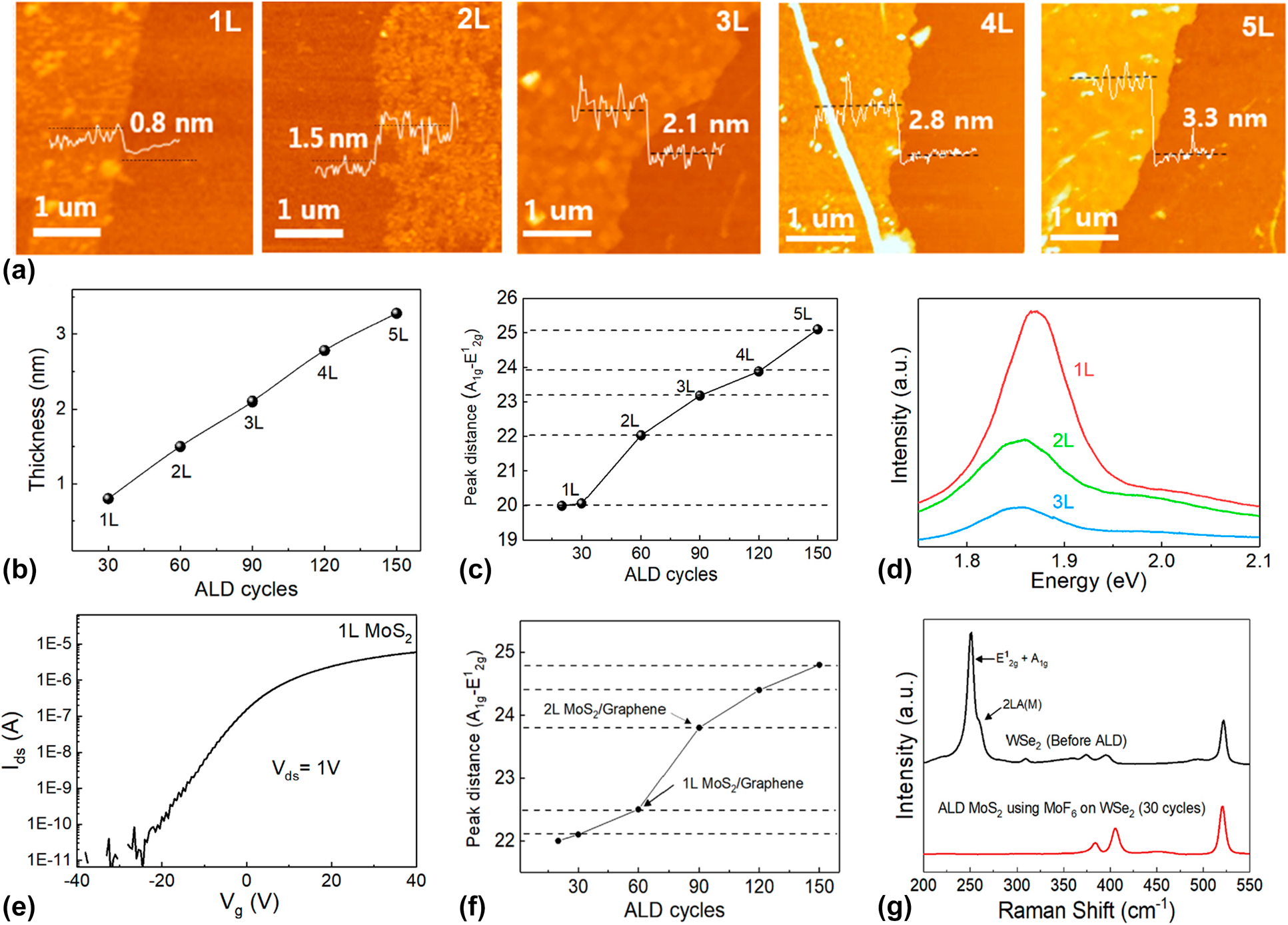
ALD MoS2 using MoF6 was also adopted for the fabrication of heterostructure with graphene and other TMDCs, WSe2 in this article. When ALD MoS2 was deposited on the CVD-grown graphene layer, the growth of monolayer MoS2 was confirmed when the number of ALD cycles was 60 by Raman analysis [Fig. 10(f)]. After the synthesis of MoS2 on graphene, 30 cycles of ALD were required for the additional MoS2 layer synthesis on the MoS2/graphene heterostructure. The longer ALD cycle for the synthesis of MoS2 on graphene was caused by the chemical inertness of the graphene layer, which requires longer nucleation delay than that on the SiO2 substrate [Reference Kim, Lee, Johnson, Tanskanen, Liu, Kim, Pang, Ahn, Bent and Bao191]. In the case of MoS2 synthesis on graphene using the MoCl5 precursor, which was abbreviated as SLS MoS2 in the previous paragraph, no MoS2 growth on graphene was observed even after 150 cycles of ALD, indicating that MoF6 is a suitable precursor for synthesizing MoS2 on carbon-based 2D materials. By utilizing this MoS2/graphene heterostructure, they fabricated an excellent photodetector without external gate voltage in operation, demonstrating the suitability of the MoS2/graphene heterostructure for optoelectronic devices.
In the case of ALD MoS2 on WSe2 using MoF6, the growth behavior was different from that on graphene. In the Raman spectra, as shown in Fig. 10(g), WSe2 peaks disappeared after 30 cycles of ALD MoS2 using MoF6 and H2S at 700 °C, indicating an etching of the WSe2 layer during the ALD process. The Raman peaks of WSe2 clearly disappeared after MoF6 exposure for 1 min at 700 °C, whereas high-temperature sulfurization using H2S showed no etching of the WSe2 layer until 1100 °C [Reference Ko, Lee, Park, Kim, Woo, Kim, Song, Park, Kim, Lee and Kim192], indicating that MoF6 etched the underlying WSe2 layer at 700 °C. Thus, ALD MoS2 using MoF6 is not suitable for synthesizing a heterostructure with other TMDC materials, thus indicating that further research on ALD TMDCs with various precursors should be conducted.
In this section, synthesis and characterization of 2D TMDCs by using ALD are discussed. Because of their inherently superior characteristics, the development of TMDC synthesis is expected to lead to a breakthrough in electronics, enabling the fabrication of next-generation nanoscale devices, such as neuromorphic computing devices [Reference Sangwan, Lee, Bergeron, Balla, Beck, Chen and Hersam36]. Among various synthetic methods, ALD-based 2D TMDC syntheses, including chalcogenization of ALD-grown metal oxides and direct ALD synthesis, have several advantages, including large-area uniformity and excellent layer controllability, which are prerequisites for mass production. In addition, the electrical and optical properties of TMDC nanosheets could be easily modulated by simply changing the composition ratio of TMDC by the ALD supercycle method. Despite these advantages, further research should be conducted for improvement in the properties of ALD-grown 2D TMDCs, to an extent that is comparable to exfoliated TMDCs. Furthermore, systematic investigation on the dependence of different deposition mechanisms of 2D TMDCs on precursors is also required. Through these efforts on the synthesis of 2D TMDCs by ALD, great advances in electronics and optoelectronics can be expected in the near future.
Conclusion & outlook
As discussed in this review, a rise of nonconventional materials using ALD can change the current paradigm of electronics, owing to their great potential to be universally applied. The versatility and unique properties of ALD allow the development of nonconventional materials, which can be applied not only to the applications suggested in this review but also to diverse fields not yet under consideration. Although the development of these materials has been limited because of the low demand from the industry, it can be expected that as downsizing of devices continues and new concepts of devices emerge, this research area will grow. The problem is only a limited number of ALD processes have been developed for these new materials. One of the main reasons for the lack of systematic research is immature precursor development for these materials. Thus, development of new precursors with various functional groups is a prerequisite for the facile growth of nonconventional materials by ALD. These studies must identify techniques for preventing various drawbacks, including abnormal growth characteristics, impurity incorporation, or damage by deleterious by-products after the ALD reaction. Consequently, intensive studies on the deposition of new materials should be carried out. The research effort would in turn open a new horizon in materials research on nonconventional material synthesis using ALD.
Acknowledgments
This work was supported by the Materials and Components Technology Development Program of MOTIE/KEIT [10080527, Development of commercialization technology of highly sensitive gas sensor based on chalcogenide 2D nanomaterial], by the Commercialization Promotion Agency for R&D Outcomes (COMPA) funded by the Ministry of Science and ICT (MSIT) [Development of Plasma-based Synthesis Equipment and Process for Two-Dimensional TMDCs], and by the Technology Transfer and Commercialization Program through INNOPOLIS Foundation funded by the Ministry of Science and ICT (2019-GJ-RD-0072/Equipment and Process Development of Large scaled 2D Nanomaterial Synthesis).


