


Introduction
Developing micromechanical testing techniques to measure the mechanical properties of materials at the microscopic scale has become a primary interest for a wide range of applications, such as thin film technology, microelectromechanical systems (MEMS) and composite materials. The mechanical properties of micro- and nanoscale components can differ significantly from bulk material, as they are affected by factors like fabrication process [Reference Nix1], material architecture [Reference Lakes2], crystal size [Reference Hall3], dimensional constraints [Reference Arzt4], and surface characteristics [Reference Judy5]. Micromechanical testing allows for improvements in miniaturized components design and may be used to better understand dimensional size effects, deformation mechanisms, as well as crack growth and propagation at small-length scales [Reference Uchic, Dimiduk, Florando and Nix6, Reference Maeder, Mook, Niederberger and Michler7, Reference Gianola, Van Petegem, Legros, Brandstetter, Van Swygenhoven and Hemker8, Reference Kiener and Minor9, Reference Nan, Wang, Misra and Huang10, Reference Ast, Przybilla, Maier, Durst and Göken11, Reference Jaya, Kirchlechner and Dehm12]. In the last decades, micropillar compression and nanoindentation have gained importance due to their relatively straightforward execution on a wide variety of materials. While it is highly informative to measure the micromechanical properties of a material in tension, developing a simple, accessible and yet accurate microtensile testing methodology has proven to be very challenging [Reference Gianola and Eberl13]. Although several microtensile techniques have been developed to answer specific questions [Reference Johanns, Sedlmayr, Sudharshan Phani, Mönig, Kraft, George and Pharr14, Reference Tian, Cheng, Shan, Li, Wang, Han, Sun and Ma15, Reference Han and Saif16, Reference Hazra, Baker, Beuth and De Boer17, Reference Liu, Wang, Li, Ding and Yang18, Reference Smolka, Motz, Detzel, Robl, Griesser, Wimmer and Dehm19], a generally accepted approach applicable to a large number of materials and comparable with macroscopic tensile testing is still missing.
Several issues arise when standardized tensile testing methodologies are brought from the macroscale to the microscopic world. Sample fabrication, specimen handling and misalignment are the most challenging issues [Reference Philippe, Schwaller, Bürki and Michler20]. Experimenting at the microscale requires attentive care during specimen preparation, as the fabrication processes can influence mechanical properties [Reference Yi, Li and Kim21, Reference Kiener, Motz, Rester, Jenko and Dehm22, Reference Chen, Wehrs, Michler and Wheeler23]. Specimen handling is a major concern since manipulating a miniaturized specimen is highly complex and could lead to premature damage [Reference Johanns, Sedlmayr, Sudharshan Phani, Mönig, Kraft, George and Pharr14, Reference Sharpe and Gad-el-Hak24]. Techniques, such as tensile chip fabrication and cofabrication of both specimen and testing setup have been adopted in the past to overcome these issues [Reference Liu, Wang, Li, Ding and Yang18, Reference Haque and Saif25, Reference Haque and Saif26]. Nonetheless, these techniques often require complex setups and exclusively rely on material specific fabrication methods, limiting the assessment of mechanical properties to only a few specific materials. Attaching a microscopic specimen to a testing setup using an adhesive (i.e., through FIB induced platinum deposition) might induce measurement errors, due to the deformation of the latter [Reference Zhang, Breguet, Clavel, Phillippe, Utke and Michler27]. On the other hand, specimen clamping might result in high forces at the edges, therefore risking failure in the early stages of a mechanical test. Additionally, a misfit between specimen and gripping surfaces [Reference Kang and Saif28] will cause unwanted bending. Misalignment between the testing apparatus and the specimen can lead to significant errors and has been found to be one of the most critical factors in micromechanical testing [Reference Kang and Saif28, Reference Zhang, Schuster, Wei and Ramesh29, Reference Niederberger, Mook, Maeder and Michler30, Reference Soler, Molina-Aldareguia, Segurado, Llorca, Merino and Orera31]. Finally, specimen design should include smooth transition zones to avoid premature failure due to stress concentrations [Reference Malhaire, Seguineau, Ignat, Josserond, Debove, Brida, Desmarres and Lafontan32], especially when the tested material is brittle. Thus, sample and tensile setup alignment should be optimal. As there is a clear need for defining a technique that works accurately and reliably, regardless of the tested material, other solutions must be sought.
In the past 15 years, FIB technology has shown to be a promising tool for the fabrication of micrometer-size features and it has been used to fabricate a variety of different mechanical specimens: compression [Reference Uchic and Dimiduk33, Reference Schwiedrzik, Taylor, Casari, Wolfram, Zysset and Michler34, Reference Dubach, Raghavan, Löffler, Michler and Ramamurty35], bending [Reference Gong and Wilkinson36, Reference Iqbal, Ast, Göken and Durst37, Reference Massl, Thomma, Keckes and Pippan38], and tension [Reference Kim and Greer39, Reference Kiener, Grosinger, Dehm and Pippan40, Reference Dehm41]. Although ion milling produces fabrication artifacts, such as damaged layers, ion implantation, curtaining, rippling, tapering, and re-deposition, these artifacts can be effectively reduced by optimizing beam settings and by using dedicated milling strategies [Reference Giannuzzi and Stevie42]. Beside its high resolution, FIB milling has the advantage of being a versatile technique, as virtually any material that remains stable in high vacuum and under the influence of electron beams can be manufactured in this way. Many biological materials, e.g., bone [Reference Schwiedrzik, Raghavan, Bürki, Lenader, Wolfram, Michler and Zysset43] or wood [Reference Schwiedrzik, Raghavan, Rüggeberg, Hansen, Wehrs, Adusumalli, Zimmermann and Michler44] have been successfully tested via micropillar compression using this technique. Combining FIB fabrication methods with a simple and widely accessible methodology for tensile testing, able to account for the potential pitfalls listed above, would allow to extend the profound knowledge on micromechanical behavior of materials under compression with systematic microtensile studies. This, in turn, would allow probing tension–compression asymmetry of size effects.
In this study, a microtensile methodology is presented. A microtensile specimen geometry is optimized through FE modeling to match the stress profile of macroscopic geometries defined in international standard ASTM D638 [45]. Additionally, FE methods are employed to improve a self-aligning microtensile gripper geometry, thus reducing the misalignment sensitivity of the setup. Two variants of gripper were produced using two different high-throughput fabrication methods for the fabrication of nanocrystalline nickel (nc-Ni) and single-crystal Si grippers. Their functionality is validated on single-crystal Si specimens. The methodology is then used to study the tension–compression strength asymmetry on the microscale in GaAs single crystals. FIB milling is used to fabricate self-standing tensile specimens and micropillars into a bulk sample. Successively, the deformation mechanisms are observed for each loading mode using scanning transmission electron microscopy (STEM) and transmission Kikuchi diffraction (TKD) on the deformed specimens.
Microtensile setup design
Sample geometry
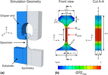
Specimen geometry was optimized through FE modeling. The goal of the simulations was to define a specimen geometry attached to a macroscopic substrate whose stress profile was comparable with the one found in the macroscopic testing geometry defined in ASTM D638 Type V [45]. Three-dimensional FE calculations were performed using the commercial solver ABAQUS/Standard (Dassault Systems, Providence, Rhode Island). To save computational time, only a quarter of the geometry was modeled and symmetry boundary conditions were applied. Longitudinal displacement was imposed by a rigid body representing the tensile gripper. A hard contact and a friction coefficient of 0.1 were assumed between the two contact surfaces. The tensile specimen was modeled as an isotropic solid with Young’s modulus E = 130 GPa and Poisson’s ratio ν = 0.3. All simulations included a part of the substrate underneath the specimen to take into account the effect of substrate deformation during tensile loading. An example of this process is shown in Fig. 1(a). The model was meshed with reduced integration linear hexahedral elements (C3D8R), and mesh convergence was reached when doubling in mesh density resulted in a change of maximum von Mises stress of less than 0.5%. Specimen geometry was optimized with respect to junction radius r, thickness t, gauge width w and gauge length l. The effect of these parameters on stress concentrations was quantified by K c. The latter was expressed as the ratio between the maximum stress at the junction σmax and the stress in the center of the sample gauge σgauge, as illustrated in Fig. 1(b).
 $${K_{\rm{c}}} = {{{\sigma _{\max }}} \over {{\sigma _{{\rm{gauge}}}}}}\quad .$$
FE model (a) and normalized von Mises stress distribution σ/σmax in the optimized dumbbell tensile sample (b). The specimen geometry has two symmetry planes with normal vectors x 1 and x 3. Therefore, the simulations were performed with only one quarter of the geometry. In (b), half of the sample is represented to facilitate interpretation. Red arrows indicate the position of maximum stress σmax, as well as the center of the gauge section. Dimensions are expressed in µm.
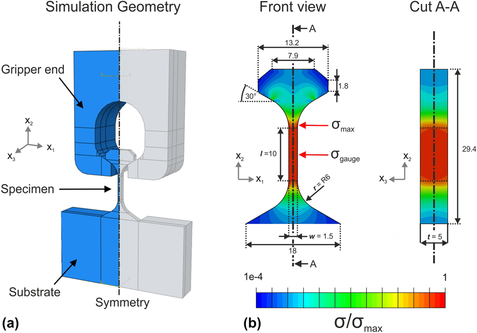
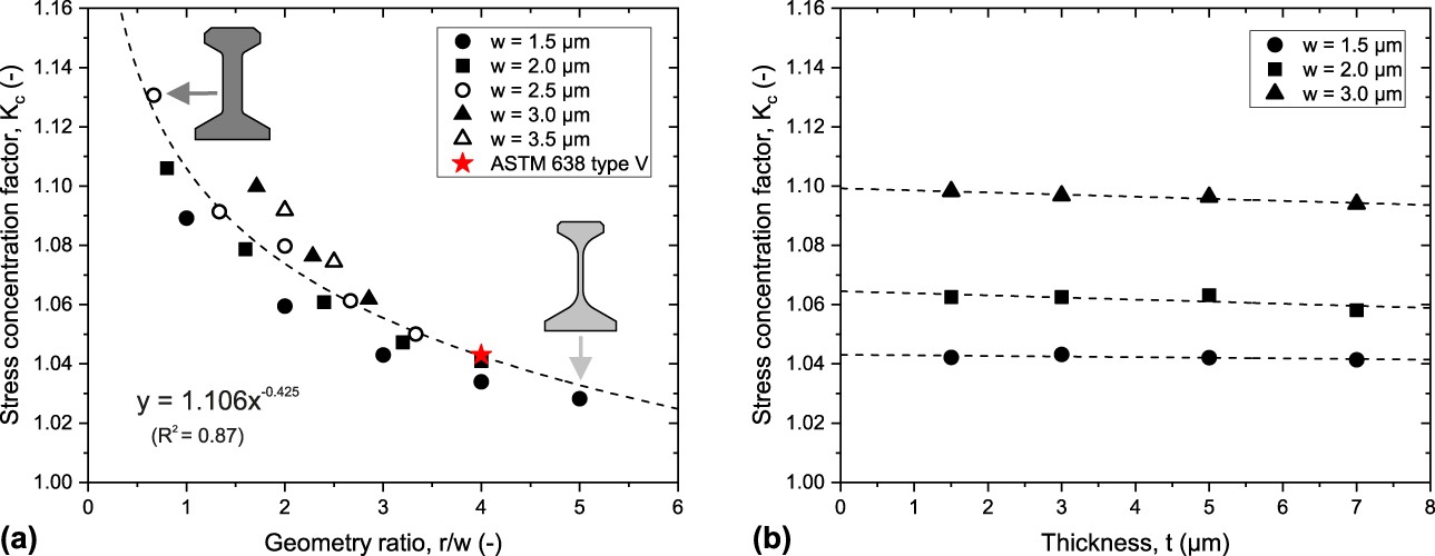
The minimum stress concentration factor was found when the ratio of the fillet radius to the gauge width was maximized. This relationship is in line with the observations by Feng et al. for free-standing tensile specimens [Reference Feng and Jasiuk46], and it can be observed in Fig. 2(a). Acceptable values of K c (<5%) are found when the junction radius to sample width ratio is equal or larger than 4. For a chosen width of 1.5 µm, the junction radius has to be 6 µm to have less than 5% of stress concentration. Gauge length was set to 10 µm to limit specimen full height below 30 µm. K c was found to be independent of thickness, as noticeable in Fig. 2(b). Specimen thickness was set to 5 µm, hence defining a rectangular cross-sectional area for the specimen gauge. There are two main advantages for this choice: (i) a thicker microtensile geometry allows for a better redistribution of the contact load on the sample head and (ii) the gain in specimen stiffness improves the load signal-to-noise ratio, while preserving strength size effects attributed to the smallest relevant dimension in the sample (thinness effect) [Reference Jennett, Ghisleni and Michler47]. Finally, the specimen head featured two 30° flanks to promote sliding of the self-aligning gripper. The final microtensile geometry, as well as the von Mises stress distribution in the loaded state, is illustrated in Fig. 1(b).
(a) Stress concentration factor K c as a function of the ratio r/w between fillet radius r and gauge width w. The stress concentration factor of ASTM 638 type V geometry has been included as a reference (in red); (b) Stress concentration factor K c showing no significant variation with sample thickness t.
Gripper geometry
The microtensile gripper was designed based on four main requirements: the gripper features (i) a keyhole-like end geometry for which specimen gripping can be achieved through mechanical contact with the lower surfaces of the sample head, (ii) a thick base allowing macroscopic handling, alignment and fixation to a customized holder, (iii) a thin and compliant end allowing for self-alignment with the sample axis [Reference Robert Wheeler, Shade and Uchic48], and (iv) the gripper should be manufactured efficiently in large numbers with a high degree of accuracy and reproducibility.
To identify which geometry would best fit these requirements, an FE study was conducted by characterizing the effect of gripper lateral compliance with respect to in-plane and out-of-plane tilting and translational misalignments. FE calculations were combined with analytical modeling, based on the Euler–Bernoulli beam theory, to improve computational time. The needle-shaped end of the gripper, represented in Fig. 3(a), was considered as a cantilever with variable cross section (along the x 2 axis). In this way, both in-plane and out-of-plane flexural deflection were determined upon an arbitrary loading of 1 mN by integrating the Euler–Bernoulli beam differential equation twice:
 $${{{{\rm{d}}^2}w\left( {{x_2}} \right)} \over {{\rm{d}}{x_2}^2}} = - {{M\left( {{x_2}} \right)} \over {E{I_{{x_1},{x_3}}}\left( {{x_2}} \right)}}\quad ,$$
where w(x) is the beam deflection, E refers to the Young’s modulus, M(x) is the bending moment, and  ${I_{{x_1}}}$ and ${I_{{x_3}}}$ are the second moment of area about the x 1 axis (in-plane) and x 3 axis (out-plane). All parameters depend on the position along the gripper length along the axis x 2. Fixed-end boundary conditions were applied at the start of the curvature radius between the base of the gripper and the needle in the front. Flexural stiffness k beam was defined by the following equation:
 $${k_{{\rm{beam}}}} = {F \over {w\left( L \right)}}\quad ,$$
where F is the force applied at the gripper end L. To simplify the analysis, each gripper geometry was associated with an equivalent beam geometry having constant cross section and sharing the same flexural stiffness of the complex and curved geometry described in Fig. 3(a). The equivalent beams were then implemented in the FE model using beam elements to characterize the influence of misalignment. This process was performed to save computational time, while keeping the number of elements relatively low.
(a) Schematics showing gripper geometries with different lengths of the compliant needle leading to an increase in lateral stiffness from left to right. The gripper features a large base to facilitate handling and fixation, while the needle in the front is responsible for gripping the actual specimen and self-align with its main axis. (b) Stress inhomogeneity factor in the specimen due to in-plane transitional and tilting misalignment as a function of the lateral gripper stiffness normalized by the lateral specimen stiffness.
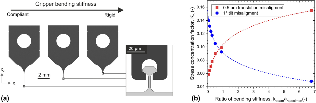
The beams were kinematically coupled to the gripper end, defined in Fig. 1(a), to guarantee a realistic interface with the sample. The top of the equivalent beam was subjected to an upward displacement of 1 µm. The same contact conditions between the sample and gripper surfaces were adopted from the simulations described in the previous section. However, in this case, quadratic elements (C3D20R and B32) were preferred over linear elements. The specimen was modeled as a perfect plastic material having isotropic elastic modulus, Poisson’s ratio, and yields stress of E = 200 GPa, ν = 0.3, and σy = 1.5 GPa, respectively. Both beam and gripper end were modeled with the material properties of single-crystal Si having the main axis aligned with its 〈100〉 crystallographic orientation (C 11 = 165.6 GPa, C 12 = 63.9 GPa, and C 44 = 79.5 GPa [Reference Hopcroft, Nix and Kenny49]). Since the main objective of this study was to primarily minimize the effect of in-plane misalignment, gripper misalignment sensitivity was initially characterized with respect to the gripper in-plane flexural stiffness for misalignments of 1° and 0.5 µm as these values have been typically reported in micromechanical tests [Reference Zhang, Schuster, Wei and Ramesh29, Reference Kiener, Grosinger, Dehm and Pippan40, Reference Kiener, Motz and Dehm50]. A stress homogeneity factor K b was used to quantify the importance of bending stress in the sample:
 $${K_{\rm{b}}} = {{\sigma _{{x_2}}^{\max }} \over {\sigma _{{x_2}}^{{\rm{average}}}}}\quad ,$$
where  $\sigma _{{x_2}}^{\max }$ is the maximum stress in the sample along its principal axis x 2 and $\sigma _{{x_2}}^{{\rm{average}}}$ is the average stress calculated by dividing the force on the sample by the cross-sectional area of the gauge section. The stress homogeneity factor was calculated during the elastic response for $\sigma _{{x_2}}^{{\rm{average}}} = 0.5\;{\rm{GPa}}$ using different gripper geometries. The relationship between K b and the ratio between gripper and specimen flexural stiffness is shown in Fig. 3(b). Based on this preliminary analysis, we selected the gripper geometry corresponding to the compromise between translational and tilting misalignment for further characterization. In this second step, in-plane misalignments up to 0.5 µm and 2° were simulated, while out-of-plane misalignments were analyzed in two specific cases: when testing the specimen at the edge of the gripper and when a 2° out-of-plane misalignment is present. Engineering stress was computed by dividing the force by the initial cross-sectional area of the gauge section, and engineering strain was extrapolated by dividing the gauge displacement by its initial length. True stress–strain data were computed using the assumption of negligible volume change [Reference Jones and Ashby51]. Stress–strain curves were offset so that the fit on the linear loading slope intersected the origin. Young’s modulus was deduced from this linear response, while yield stress and strain where determined using the 0.2% strain offset method.
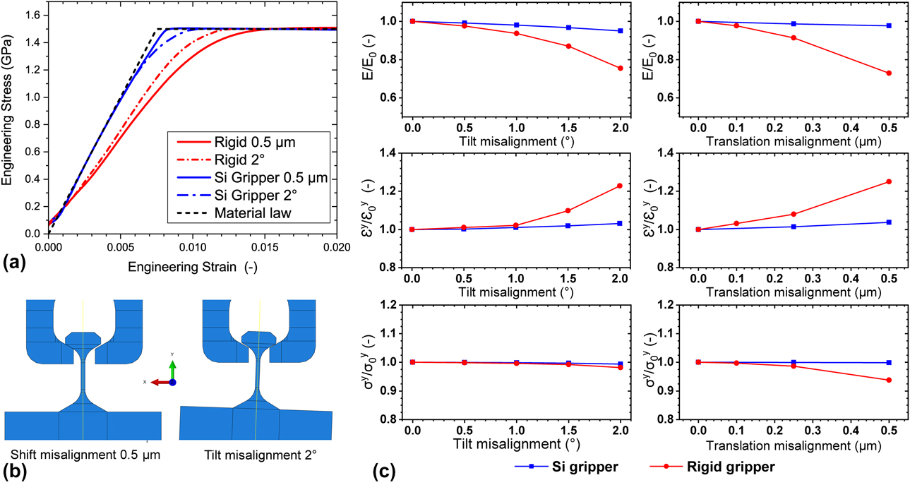
Conflicting trends were found for translational and tilting misalignments: a laterally compliant gripper is tolerant to translation misalignment; however, it produces more stress heterogeneity in the specimen gauge section when tilt misalignment is present. For a stiff gripper, the opposite is true. Depending on the ratio of gripper to sample lateral stiffness, the ultimate tensile strength may be underestimated with an error between 5 and 16%. The error increases significantly with the degree of misalignment. It is important to state that this result is most relevant when investigating the tensile strength of brittle materials, for which failure is dominated by the stress concentrations within the sample. Ductile materials will be less susceptible to these stress concentrations. Gripper geometry representing the intersection between the two curves was selected for the successive step. For the latter, the stress–strain curve displayed in Fig. 4(a) highlights the advantages of using laterally compliant grippers instead of a rigid gripper. When a rigid gripper is used, there is a significant reduction of measured elastic modulus, regardless of the type of misalignment, for both brittle and ductile specimens. In contrast, the compliant gripper can correct both types of misalignment after an initial stage of adaptation (toe region), resulting in a more accurate stress–strain characterization. The selected compliant gripper ensures less than 5% error for misalignment up to 2° and 0.5 µm (1/3 of the sample gauge width). Although the simulations showed that a stiff gripper may be used to measure the yield stress of a plastic material even in the case of small misalignments (within an error of approximately 10%), they also showed that the error for yield strain, as well as for elastic modulus, exceeds 25%, as observed in Fig. 4(c). When the specimen is tested along the edge of the gripper (out-of-plane translational misalignment), the elastic modulus is underestimated by 15.6% and this scenario will produce a stress homogeneity factor K b of 1.07. Whereas a 2° out-of-plane tilt misalignment results in an error of 14.4% for elastic modulus measurement and produces a stress inhomogeneity factor K b of 1.22. In conclusion, a laterally compliant gripper is a better choice when yield strain or postyield behaviors are of interest. The gripper geometry adopted for this study is shown in Fig. 5(b).
(a) Misalignment sensitivity for a rigid gripper and compliant Si gripper used in this study for a 0.5-µm translational misalignment and 2° tilting misalignment on a simulated ductile specimen with E = 200 GPa and σy = 1.5 GPa. Resulting stress–strain curves are compared with the material law used in the simulations. (b) Schematics depicting the simulated misalignment types: in-plane tilting and translational misalignment. (c) Changes in normalized elastic modulus (top), yield strain (middle), and yield stress (bottom) measured from the simulated stress–strain response in presence of misalignments for a rigid gripper and then a compliant Si gripper.
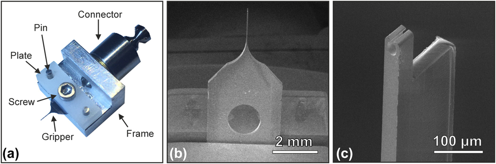
(a) Aluminum gripper holder used to fix and align the microtensile gripper with the nanoindenter longitudinal axis. The alignment is made by contacting the backside of the gripper with a 200-µm step in the aluminum holder, while fixation is achieved through friction by screwing a polyoxymethylene (POM) plate to the gripper. A connector piece is used to replace the nanonindentation tip with the tensile gripper holder in the micromechanical testing platform (see Fig. 6); (b and c) SEM images of a silicon microtensile gripper. The last 150 μm of the compliant needle have been reduced to a thickness of 50 μm by a Xe plasma FIB.
Stress–strain measurement
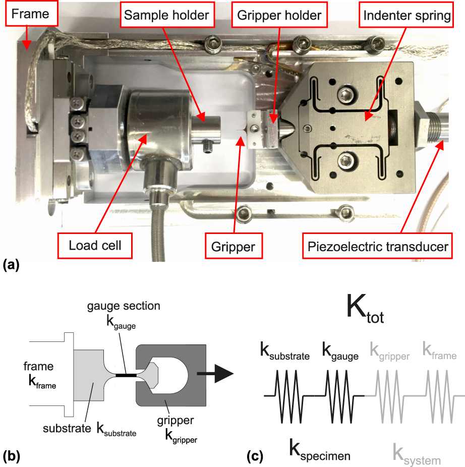
When using the presented setup, stress–strain data can be obtained from the experimental data through a compliance correction. The measured displacement corresponds to the sum of the deformations of the specimen and the tensile setup.
 $${d_{{\rm{tot}}}} = {d_{{\rm{specimen}}}} + {d_{{\rm{system}}}}\quad .$$
By considering the entire setup as a set of springs in series as shown in Fig. 6(c), one can express the following relationship:
 $${1 \over {{k_{{\rm{tot}}}}}} = {1 \over {{k_{{\rm{specimen}}}}}} + {1 \over {{k_{{\rm{system}}}}}} = {1 \over {{k_{{\rm{gauge}}}}}} + {1 \over {{k_{{\rm{substrate}}}}}} + {1 \over {{k_{{\rm{system}}}}}}\quad ,$$
where k tot is the stiffness of the entire apparatus and it is given by the linear regression of the unloading slope of the force–displacement data, k system corresponds to the stiffness of all the elements that do not change between experiments (i.e., gripper and indenter frame compliance), while k gauge and k substrate relate to the stiffness of the gauge section and the underlying substrate, respectively. For any given specimen geometry under uniaxial tension along the x 2 direction (longitudinal axis), the gauge stiffness is proportional to the elastic modulus  ${E_{{x_2}}}$ in this direction. In the case of an isotropic material, ${E_{{x_2}}}$ is equal to the Young’s modulus E. For the geometry defined in Fig. 1(b), the gauge stiffness is equal to
 $$k_{{\rm{gauge}}}^0 = {C_1}{E_{{x_2}}}\quad ,$$
where C 1 = 0.750 µm, and it is the constant ratio between gauge stiffness and gauge elastic modulus. This coefficient was found by monitoring the results of force and displacement at the edges of the gauge length calculated via FE for different moduli (R 2 = 1). Similarly, FE calculations made also possible to express a linear dependency (R 2 = 1) between specimen stiffness and specimen modulus  ${E_{{x_2}}}$:
 $$k_{{\rm{specimen}}}^0 = {C_2}{E_{{x_2}}}\quad ,$$
where C 2 = 0.398 µm and represent the ratio between specimen stiffness and specimen elastic modulus. Additional FE simulations were performed to account for imprecise specimen manufacturing. Geometry correction factors were determined to express sample and gauge stiffness changes in the case of geometrical deviations up ±0.5 µm for both thickness (∆t) and width (∆w) from the dimensions specified in Fig. 1(b). For this, eight additional simulations were performed. A 3D surface was fitted (R 2 > 0.99) using MATLAB (MathWorks, Natick, Massachusetts), and geometry factors were defined as follows:
 $${f_{{\rm{gauge}}}}\left( {\Delta t,\Delta w} \right) = {{{k_{{\rm{gauge}}}}} \over {k_{{\rm{gauge}}}^{\rm{0}}}} = \left( {1 + {{\Delta t} \over {{t_0}}}} \right)\left( {1 + {{\Delta w} \over {{w_0}}}} \right)\quad ,$$
 $${f_{{\rm{specimen}}}}\left( {\Delta t,\Delta w} \right) = {{{k_{{\rm{specimen}}}}} \over {k_{{\rm{specimen}}}^{\rm{0}}}} = \left( {1 + {{\Delta t} \over {{t_0}}}} \right){\left( {1 + {{\Delta w} \over {{w_0}}}} \right)^{0.783}}\quad ,$$
where t 0 and w 0 represent the ideal cross-sectional dimension: 5 µm and 1.5 µm, respectively. Young’s Modulus can be computed by inserting Eqs. (10) and (8) into Eq. (6):
 $$Ex<sub>2</sub> = {{{f_{{\rm{specimen}}}}} \over {0.398}}{\left( {{1 \over {{k_{{\rm{tot}}}}}} - {1 \over {{k_{{\rm{system}}}}}}} \right)^{ - 1}}\quad .$$
(a) Microtensile setup consisting of an in situ nanoindenter for which the indentation tip has been replaced with the tensile gripper holder described in Fig. 5(a). A piezoelectric transducer is used to apply a prescribed displacement on the gripper by movement of the indenter spring. Tensile displacements are realized by applying a pretension on the spring and retracting the piezo throughout the experiment. (b) Schematic representation of the system in terms of mechanical components contributing to machine compliance. The simplified system consists of four main elements: frame, substrate, gauge section, and gripper. The mechanical component frame includes the instrument frame, load cell, sample holder, indenter spring, piezoelectric transducer, gripper holder, as well as positioning axes for sample positioning. (c) Based on these simplifications, a mechanical analogon can be defined consisting of a set of springs in series describing the stiffness of the whole mechanical system as a function of the respective subsystem stiffness.
This relationship assumes that the system compliance is known and that the measurement of k tot is made during the purely elastic response. The calibration of the system can be executed by testing reference specimens, for which the Young’s modulus is well-known (i.e., single crystals with known orientation). For the extrapolation of the gauge section displacement, it is assumed that all of the elements in the tensile setup, excluding gauge section, deform elastically. If this is the case, the displacement of the gauge section may be expressed as follows:
 $${d_{{\rm{gauge}}}} = {d_{{\rm{tot}}}} - F\left( {{1 \over {{k_{{\rm{tot}}}}}} - {1 \over {0.75{Ex<sub>2</sub>}{f_{{\rm{gauge}}}}}}} \right)\quad .$$
Once the displacement in the gauge section has been calculated, the engineering stress–strain curves are easily obtained by dividing the force by the cross-sectional area of the gauge section and by dividing the corrected displacement by the initial gauge length. True stress–strain curves are finally extrapolated by assuming negligible volume change [Reference Jones and Ashby51].
Results
Experimental characterization of the microtensile setup
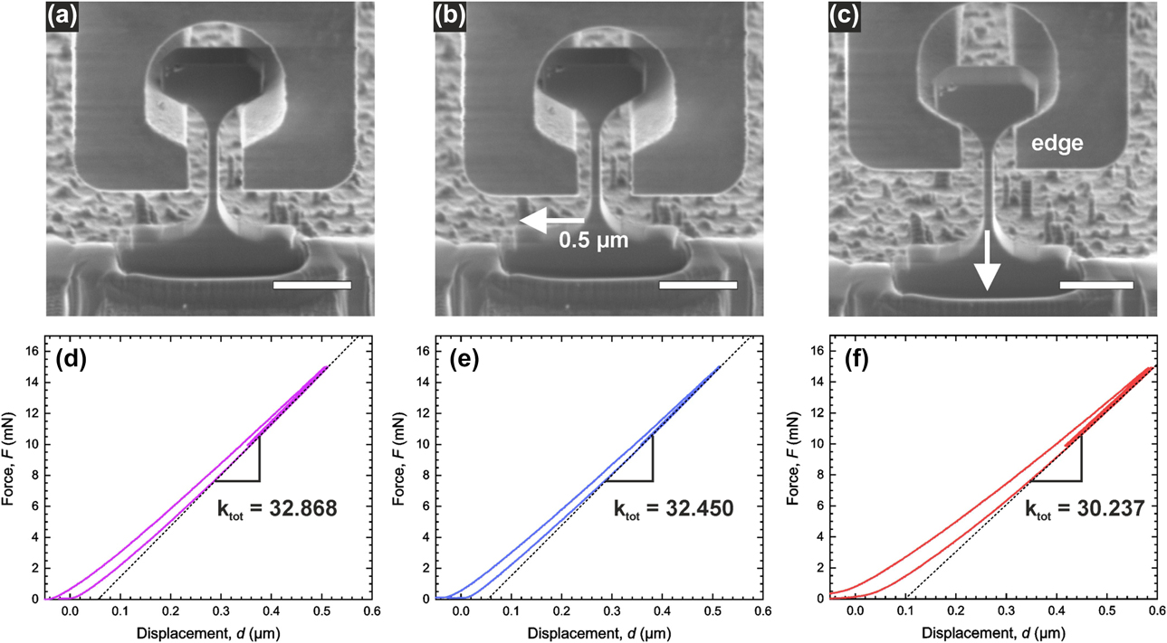
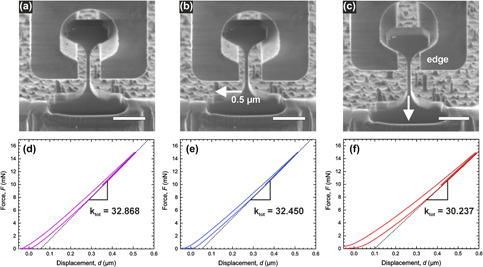
Setup compliance was found to be 13.2 ± 0.2 nm/mN when using the nc-Ni gripper and 12.9 ± 0.2 nm/mN when using the Si gripper. Based on the test performed on the Si specimens, it was noticed that the two gripper typologies exhibited differences in the apparent force–displacement data. For both typologies, the elastic loading–unloading response showed a clear difference between the loading and the unloading slope. Nevertheless, this difference was greater for the nc-Ni gripper. Loading and unloading slopes differed by approximately 25% in the case of the nc-Ni gripper and 15% in the case of the Si gripper. The nc-Ni gripper also exhibited longer adaptation periods (toe regions) before attaining a linear trend in the stress–strain curve. Figure 7 illustrates the effect of in-plane and out-of-plane misalignment on the measured stiffness. The introduction of an additional misalignment of 0.5 µm before the elastic loading–unloading cycles results in a 2.2% error on the elastic modulus. Whereas, by testing the specimen at the gripper edge, the elastic modulus is underestimated by 15.1%.
(a–c) SEM images of a single-crystal Si specimen oriented in the [001] direction of the crystal tested in different conditions. (a) Aligned, (b) in-plane translational misalignment of 0.5 μm, and (c) out of plane translational misalignment to the edge of the gripper. Scale bars represent 10 μm. (d–f) Corresponding force–displacement curves for the three different cases of misalignment. The measured total stiffness changes by 1.3% for in-plane misalignment of 0.5 µm and 8.0% for out-of-plane misalignment of 25 µm. These changes amount to a change of measured elastic modulus of 2.2% and 15.1%, respectively.
GaAs tensile tests
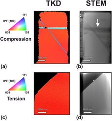
All single-crystal GaAs microtensile specimens showed brittle failure. All specimens except one failed within the gauge section. The unsuccessful test was discarded from the mechanical analysis. Stress and strain data for tensile experiments are illustrated in Fig. 8(f). The microtensile samples exhibited ultimate failure stress of 1.86 ± 0.17 GPa and ultimate strains of 3.0 ± 0.4%. The elastic modulus in the [001] crystal orientation, obtained from the unloading slope at around 1.5% strain, was 81.4 ± 4.6 GPa. Subsequent SEM imaging revealed complex curved fractures surfaces. For all specimens, the majority of the edges in the fracture surfaces were oriented within a {110} plane. Nevertheless, it was not possible to index the fracture surfaces, due to the presence of complex curvatures. STEM and TKD analysis, illustrated in Figs. 9(c) and 9(d), did not show any visible contrast, suggesting that no local plasticity occurred.
(a, b) SEM images of two GaAs micropillars tested in compression and (c, d) the fracture surface of a microtensile specimen after brittle failure. White arrows indicate visible surface steps. (e, f) Stress–strain data for micropillar compression (e) and microtensile tests (f) on GaAs with the [100] direction of the crystal aligned with the loading axis. Dotted lines denote the extension of the unloading slope, where elastic modulus was measured.
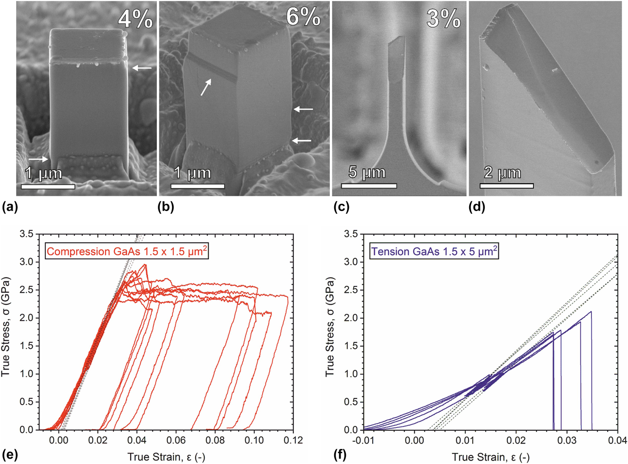
(a) TKD and (b) STEM images for a compressed micropillar. Twinning in the {111} system was identified as the major deformation mechanism by TKD. High dislocation density may be observed near twin boundaries based on bright field STEM (white arrow) (c) TKD and (d) STEM of the lower portion of a failed microtensile sample. No measurable dislocation activity was observed by either TKD or STEM in the case of tensile loading.

GaAs compression tests
Uniaxial compression tests on taper-free single-crystal GaAs micropillars revealed close to perfect plasticity. The experimental data are displayed in Fig. 8(c). The measured yield stress was 2.60 ± 0.14 GPa, and the yield strain was 3.5 ± 0.3%. The apparent elastic modulus measured on the [001] orientation was 86.5 ± 3.1 GPa. After yielding, all micropillars exhibited a consistent and reproducible plastic regime at 2.42 ± 0.11 GPa, with no apparent hardening. Seven out of eleven micropillars showed a clear stress drop of a few hundred MPa before reaching the constant stress regime. STEM imaging performed on a micropillar compressed to 5.1% strain, seen in Fig. 9(b), showed two main contrast bands and the presence of multiple dislocations. The first contrast band was oriented perpendicularly to the loading direction, while the second was oblique at an angle of 36.27° with respect to the pillar [001] axis and had a thickness of approximately 80 nm. A surface step was observed in the amorphous layer of the pillar at the end of the second contrast band. TKD analysis, observed in Fig. 9(a), established that these bands correspond to crystal twinning in two different {111} planes. Assuming a perfect alignment between the [001] axis and the loading axis, the resolved shear stress on the {111} planes was found to be 1.0 ± 0.1 GPa. Finally, it is worth noting that the FIB-produced amorphous layer was visible in Bright-field (BF) STEM, where its thickness less than 25 nm.
Discussion
A microtensile testing methodology was developed based on a novel specimen geometry and gripper design to both minimize stress concentrations and misalignment sensitivity. Specimen geometry was designed so that it can be manufactured at the edge of a bulk sample and tested without the need of difficult manipulations. The ratio between specimen junction radius and specimen width should be maximized to reduce stress concentrations. FE simulations showed that a ratio of 4 to 1 limits the stress concentrations in the sample to less than 5%. The stress profile illustrated in Fig. 1(b) was found to be comparable with the specimen geometry defined by international standard D638 type V. Specimen size can be upscaled or downscaled, as long as the ratios between geometric parameters are maintained to keep the same stress profile. In the present study, sample fabrication was achieved by FIB milling, as this technique allows micromachining of a large range of materials at high resolution.
Setup alignment was improved by using a laterally compliant gripper able to self-align with the specimen during the first stages of the tests. Euler–Bernoulli beam theory and FE have been employed in the calculations to optimize the gripper geometry. It has been shown that a laterally compliant gripper minimizes the bending in the sample during a test with initial misalignment. Two different fabrication methods were used to fabricate interchangeable grippers with similar flexural stiffness. Between the two gripper types, the Si grippers were preferred over the nc-Ni grippers. A gripper holder can be fitted easily into a commercial indenter, making this technique widely accessible. Since the system compliance reduces the displacement applied to the specimen, it was necessary to develop a compliance correction methodology to extrapolate the actual displacement applied to the specimen gauge.
Microtensile gripper performance
While two methodologies for gripper fabrication are illustrated, there are several reasons to prefer Si grippers over nc-Ni grippers. While both grippers are insensitive to initial in-plane misalignment, the Si grippers allow for a more accurate estimation of strain. When Si grippers are used, the system overestimates the total strain by a factor of 1.15 instead of 1.25. Si grippers are much easier to fabricate in a consistent way due to the high resolution achieved by reactive ion etching. The latter allow for the simultaneous production of about 100 equivalent grippers on a single 4-inch wafer. Producing a Si gripper is relatively fast and inexpensive compared with nc-Ni, as the latter requires extensive FIB milling. For the fabrication of the nc-Ni grippers, it is indeed necessary to directly mill the keyhole opening, as the LIGA process does not have the resolution necessary to directly produce very small features (5 µm) consistently. FIB milling on the gripping surfaces can introduce two main side effects: increased surface roughness and possible asymmetries. Both effects could be responsible for the longer initial adaptation or toe region observed in the force–displacement data with the nc-Ni grippers. Finally, single-crystal Si is not affected by creep at room temperature. In contrast, pure nc-Ni, like most pure nanocrystalline materials, exhibits room temperature creep behavior above 600 MPa [Reference Wang, Wang, Aust and Erb52, Reference Yin, Whang, Mirshams and Xiao53] and might not be suitable when testing strong materials. Based on all of these reasons, it was chosen to continue the study only with the Si grippers.
System advantages and limitations
The main advantage of having a laterally compliant gripper was demonstrated with the Si reference samples. The laterally compliant gripper tends in fact to self-align with the sample axis when initial misalignment is introduced, allowing an accurate measurement of mechanical properties. For the calibration samples, in-plane misalignment of 0.5 µm (corresponding to 1/3 of the samples width) resulted in only 2.2% difference in elastic modulus (similarly to what predicted from FE calculations). For a similar degree of misalignment, a rigid tensile system [Reference Kim and Greer39, Reference Kiener, Grosinger, Dehm and Pippan40] would lead to an error of up to 30% of strain and modulus (Fig. 4). Although a five-axis control system might be used to facilitate the sample positioning an alignment [Reference Uchic and Dimiduk33], this solution is not ideal in cases where the observation of the sample is limited by the resolution of the instrumentation used. It would be highly challenging, if not impossible, to precisely align a sample and a gripper ex situ using a light based optical system. Contrarily, the compliant gripper described here would facilitate ex situ testing as the initial misalignment has minimal influence on the mechanical data. This system, therefore, opens up the possibility of studying the tensile properties of materials at low-length scales in different environmental conditions, i.e., biological materials in controlled humidity and temperature, without having to use an SEM to image the sample during initial placement. It is, however, important to minimize as much as possible out-of-plane misalignment as the error made on the measurement of the elastic modulus in this case can go up to approximately 15%. This is, however, less likely to happen since the gripper is at least 10 times thicker than the specimen.
An error propagation analysis was conducted based on the assumption of random independent errors [Reference Taylor54] for the measured variables width w, thickness t, force F, displacement d, setup compliance k system, and also misalignment. Assuming a measurement error of 100 nm for all the geometric dimensions (t and w) [Reference Johnson, Jones and Howe55], a peak–peak noise of ΔF = 4 µN for the load cell (at 20 Hz), a displacement noise floor of Δd = 1 nm, an imprecision in the determination of k system of 10%, and an in-plane misalignment of 0.5 µm; this study revealed an uncertainty of 5.4% for the measurement of the elastic modulus.
While this can be said for the elastic modulus, the setup has an uncertainty of approximately 15% on total strain. The reason for this uncertainty is the difference between the loading and unloading slope seen during experiments. This suggests that the assumption of modeling the system as a series of linear springs is an oversimplification of the setup [Reference Kalidindi, Abusafieh and El-Danaf56]. The compliance correction assumes an ideal surface contact with no sliding between sample and gripper. Slight differences in surface topography, as well as misalignment, can lead to changes in terms of contact area as a function of the applied load. Despite these limitations, the methodology offers a practical alternative to digital image correlation (DIC), especially when a direct observation of the sample surface is impossible or experiments are performed at high strain rates.
Microtensile sample fabrication
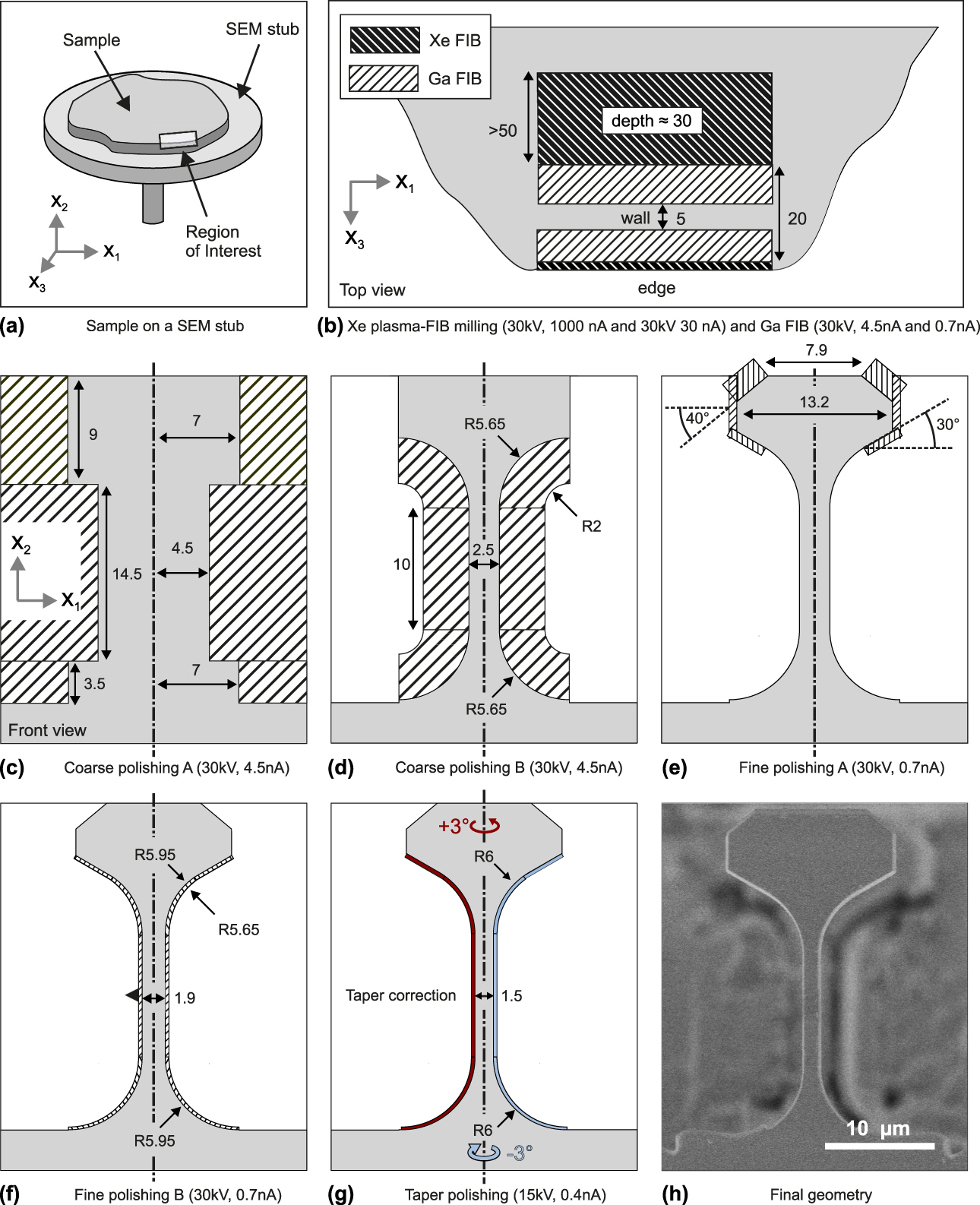
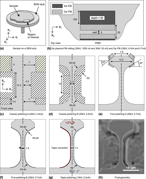
While being versatile and allowing for the fabrication of various materials, specimen fabrication via FIB milling can introduce several artifacts that might influence the mechanical response of the tested material. An important issue to consider during the specimen fabrication is the effect of FIB damage from irradiation by Ga ions on the overall mechanical response of the tested material. Using the protocol illustrated in Fig. 10, it was possible to confine the layer damaged by ion irradiation to less than 25 nm (estimated from STEM). This accounts for approximately 6% and 4% of the cross-sectional area for compression and tensile specimens, respectively. If these values are expected to significantly affect the mechanical properties of the tested material, it is possible to further lower the acceleration voltage and beam current to reduce the thickness of the FIB-induced damage layer, as well as Ga implantation, at the cost of milling rate [Reference Kato57]. Specimen clean-up with acceleration voltages as low as 5 kV has been shown to dramatically reduce both Ga penetration depth and concentration down to a thickness of 5 nm with 2 at % Ga ions in Si specimens [Reference Thompson, Gorman, Larson, Van Leer and Hong58, Reference Thompson, Lawrence, Larson, Olson, Kelly and Gorman59]. Additionally, low grazing angles during the final milling step have been reported to reduce the damaged layer thickness [Reference Burnett, Kelley, Winiarski, Contreras, Daly, Gholinia, Burke and Withers60, Reference Bals, Tirry, Geurts, Zhiqing and Schryvers61]. Another artifact to avoid is the taper on the milled surfaces. If a taper is not corrected, the real specimen geometry will deviate from the desired shape and may introduce localization of deformation. The tapering angle depends on both the beam settings and material. In this study, the taper was successfully reduced from 3° to 0.3° by overtilting both Si and GaAs specimens by 3° during the last polishing steps for both micropillars and tensile specimens. Curtaining can also appear during FIB milling, especially for deep millings. This artifact appears due to variations in specimen topography, which cause differences in sputtering rates [Reference Giannuzzi and Stevie62]. Curtaining is strongly reduced by depositing a protective cap (i.e., tungsten, platinum, or carbon) 1–2 μm in thickness on the top of the area of interest prior to FIB milling [Reference Munroe63, Reference Tomus and Ng64]. This approach may compromise the mechanical measurements during micropillar compression. However, for tensile specimens, the protective cap is deposited on a surface, which is not mechanically loaded and will not influence the measured properties. Finally, rocking the sample during milling has also been found to be effective in reducing the surface roughness [Reference Loeber, Laegel, Wolff, Schuff, Balle, Beck, Eifler, Fitschen and Steidl65].
Sketch of the FIB milling protocol for the microtensile specimen geometry. (a) Sample, (b) vertical milling, and (c–g) frontal milling. In the last step (g), the specimen is rotated by 3° and a polishing toward the surface is performed so that the taper resulting from the previous FIB process is reduced in the gauge section. The step is repeated for the opposite side. (h) Final specimen shape illustrated for a single-crystal GaAs sample, for which the longitudinal axis of the specimen is oriented in the [001] direction of the crystal. Dimensions are given in µm.
Case study on GaAs
Single-crystal GaAs has been mechanically tested along the [001] crystallographic orientation in both compression and tension on samples sharing a common thinnest dimension of 1.70 ± 0.19 µm. The elastic modulus in both compression and tension was successfully measured and was in good agreements with the value found in literature of 85.5 GPa [Reference Cottam and Saunders66, Reference Blakemore67]. While the elastic response was the same in tension and in compression, all tensile samples exhibited brittle failure, whereas all micropillars deformed plastically. At the macroscale, GaAs is typically known to have very little room temperature ductility. Brittle-to-ductile transition under uniaxial compression at room temperature has been reported for micropillars of diameters in the range of 1 µm [Reference Östlund, Howie, Ghisleni, Korte, Leifer, Clegg and Michler68, Reference Michler, Wasmer, Meier, Östlund and Leifer69]. By combining the results of this study with previous observations [Reference Östlund, Howie, Ghisleni, Korte, Leifer, Clegg and Michler68], it can be concluded that for compression, the brittle-to-ductile transition in GaAs needs to occur at sizes between 1.7 and 2.3 µm. Contrarily, brittle-to-ductile transition in tension was not observed here, but it is expected at lower length scales [Reference Bao, Wang, Cui, Gao, Yen, Liu, Kong Yeoh, Liao, Du, Hoe Tan, Jagadish, Zou, Ringer and Zheng70, Reference Chen, Gao, Wang, Liao, Mai, Tan, Zou, Ringer and Jagadish71]. Plasticity in compression was attributed to twinning formation along multiple {111} planes. This behavior has been observed also in previous studies [Reference Niederberger, Mook, Maeder and Michler30, Reference Michler, Wasmer, Meier, Östlund and Leifer69]. For zinc blende systems, such as GaAs, compression along the [001] axis generates a total of 8 slip systems  $\left\{ {111} \right\}\left\langle {1\bar{1}0} \right\rangle$ sharing the same highest Schmid factor of 0.408. A full dislocation belonging to one of these systems can dissociate in two Shockley partials [Reference Kuesters, De Cooman, Carter and Kuesters72, Reference Le Bourhis and Patriarche73]. If the dissociation distance of the two Shockley partials is larger than the length of a glide plane within the micropillar, it is possible for the leading partial to traverse the pillar and annihilate at the surface before the trailing dislocation has started to move, leaving, in turn, a stacking fault in the {111} glide plane. At room temperature and equilibrium conditions, such dissociation distance has been reported in the range of 6–13 nm [Reference Moon, Umeda and Saka74]. Nevertheless, external stresses can strongly influence this characteristic distance [Reference Lefebvre, Androussi and Vanderschaeve75]. With the high resolved shear stress calculated in this study, it is likely that the dissociation distance surpasses the length of the glide system observed in Fig. 9(b) [Reference Michler, Wasmer, Meier, Östlund and Leifer69]. The resulting stacking fault, created by the leading dislocation, can successively act as a preferential site for the nucleation of another dislocation on one of the adjacent gliding planes, leading to the formation and lateral growth of a twin [Reference Ning and Huvey76]. Taper-free micropillars showed a constant plastic flow of 2.42 ± 0.11 GPa for strain up to 12%, no hardening/softening was observed, suggesting no significant interaction of dislocations in the pillar. Possibly, most dislocation nucleates from the surface, travels across the crystal, and exits the opposite surface of the pillar. In this way, twin thickening is not associated with an increase in stress. The load drop observed in several micropillars has also been observed in GaAs produced via lithography [Reference Chen, Wehrs, Michler and Wheeler23], suggesting that this effect is not caused by the specimen fabrication. Instead, this behavior is typically attributed to low initial dislocation density [Reference Johnston77]. In an almost pure crystal, plasticity is initiated only when a certain amount of mobile dislocations are available. Once plasticity is initiated, the newly formed defects in the crystal, such as surface defects, can act as lower activation energy dislocation sources [Reference Godet, Brochard, Pizzagalli, Beauchamp and Soler78].
Tensile tests showed brittle failure. Both STEM and TKD showed no sign of dislocation nucleation, confirming our initial hypothesis of a completely brittle failure. All fractured specimens exhibited complex failure surfaces, which complicated the extrapolation of the crack dynamics. SEM imaging revealed that fracture initiation was always located at the back of the sample, where a thin amorphous layer of redeposited material from the final polishing step was located. It was noticed that most of the edges of the fractured surfaces coincided with a {110} plane, which correspond to the cleavage plane for materials with a zinc blende structure, such as GaAs. It is likely that the complicated shape of the fracture surface observed in Fig. 8(d) is caused by the competition of the {100} plane of maximum tensile stress and the {110} cleavage plane, on which cracks can easily propagate in GaAs [Reference Cook, Gordon, Evans and Marsh79]. Additionally, a sudden adaptation of the laterally compliant gripper upon a change in local stress distribution within the sample at the beginning of the fracture event could complicate even more the dynamics of failure leading to complex fracture surfaces.
The loading mode asymmetry observed in this study can be explained in terms of internal flaw dependency and fracture toughness. Cracking in brittle materials is initiated before any plasticity can occur due to the high local stress concentrations found in the vicinity of internal flaws. When the dimension of the loaded volume is decreased, the stress required for cracking increases, as less and smaller preexisting flaws will exist within a smaller sample. Below a certain size, the fracture strength of a single crystal becomes higher than the material yield strength, therefore allowing the onset of plasticity. For uniaxial tensile experiments, the loading mode preferentially leads to cracks opening in mode 1 perpendicular to the loading axis, which dramatically reduces ductility. In contrast, in compression mode 1, cracks are formed due to the formation of tensile hoop stresses [Reference Horii and Nemat-Nasser80] generated by, e.g., the geometrical constraints applied at both end of a micropillar and lead to axial splitting of the pillar. As the tensile stresses acting on the crack tips are much lower in that case, the load required for crack propagation is much higher in compression compared with tension. Therefore, although both compression and tensile samples have the same dimension, in tension, the yield stress is not attained due to the higher stress concentrations at the crack tips, which lead to catastrophic failure of the samples.
Conclusion
A general and accessible methodology allowing for uniaxial tensile testing of micron-size specimens has been presented. The microtensile setup proposed in this study can self-align with the specimen axis by using a laterally compliant single-crystal Si gripper. Si grippers may be fabricated in large batches in a very precise and reproducible manner through a photolithography-based dry etching process. This study illustrates an FIB milling protocol to fabricate tensile specimens, whose geometry has been optimized by FE modeling to replicate stress profiles comparable with macroscopic samples defined by ASTM 638. The sample fabrication process is done on a bulk substrate, so that several free-standing tensile specimens may be prepared on a single sample, therefore facilitating handling and transport. The microtensile methodology was validated on (100) Si and demonstrated experimentally by studying the tension–compression asymmetry of strength in (100) single-crystal GaAs. Clear loading mode dependence was observed when tensile tests were compared with micropillar compression experiments. For both sample types sharing the thinnest dimension of 1.70 ± 0.19 µm, GaAs showed plasticity via twinning in compression, while failing in a brittle manner in tension. While presenting a clear size effect, at this scale, GaAs is stronger in compression, reaching a plastic flow stress of 2.42 ± 0.11 GPa, while it fails in tension at 1.86 ± 0.17 GPa. STEM and TKD were used to assess deformation mechanisms in both loading modes. The experimental results showed high reproducibility and reliability for both measured elastic modulus and tensile strength, showing the potential of the novel microtensile testing methodology.
Experimental section
The microtensile testing methodology was validated on single-crystal Si specimens, while the loading mode dependency of single-crystal GaAs was characterized by means of uniaxial micropillar compression and microtensile testing.
Specimen fabrication
GaAs microtensile specimens
A small section of few millimeters side length was cleaved from a 4-inch Si-doped (2 × 1018 cm−3) GaAs (001) wafer and was mounted on a standard aluminum SEM stub using cyanoacrylate glue (Ergo 5011, Kisling AG, Wetzikon, Switzerland). The sample was coated with a thin 10-nm layer of Au using a sputter coater (Leica EM ACE600, Leica, Wetzlar, Germany). Six microtensile specimens were fabricated on the cleaved surface (110) and were oriented along the [001] axis. Crystal orientation was verified by electron backscattering diffraction (EBSD). The FIB milling process consisted of two main steps: rough milling for the fabrication of a free-standing wall and successive frontal milling to obtain the tensile geometry showed in Fig. 10(h). A Xenon (Xe) plasma-FIB (FERA3, Tescan, Brno, Czech Republic) operated at 30 kV with currents of 1000 and 30 nA was used to produce the rough cut of the wall at the edge of the bulk material, see in Fig. 10(b). Wall thickness was kept to 20 µm, ensuring at least 5 µm of undamaged material after the Xe ion milling. The walls were 30 µm tall and at least 30 µm wide. When multiple specimens were produced for the same trench, individual sections were separated by a space of 50 µm to reduce re-deposition of sputtered material onto other specimens and to facilitate maneuvering during the tests. Successively, a Ga FIB-SEM workstation (LYRA, Tescan, Brno, Czech Republic) was used to thin the wall sections down to 5 µm using an acceleration voltage of 30 kV with decreasing currents starting from 4.5 nA for coarse milling to 0.7 nA for fine milling. Frontal milling consisted of a rough cut at 30 kV and 4.5 nA followed by two polishing steps at 30 kV with 0.7 nA and 15 kV with 0.4 nA, respectively. In the last step, each side was polished individually with a 3° over-rotation to correct for taper. The complete FIB milling protocol is illustrated in Fig. 10. The six GaAs tensile specimens exhibited gauge width and thickness of 1.67 ± 0.23 µm (mean ± standard deviation) and 5.34 ± 0.23 µm.
GaAs microcompression specimens
Eleven single-crystal GaAs micropillars with square cross-sections were machined with a Ga FIB-SEM workstation. Rough cuts were performed at 30 kV with currents of 4.5 nA, while fine milling was performed at 30 kV at 200 pA. A 3° over-tilt polishing was performed for each of the 4 sides at acceleration voltages of 15 kV and currents of 50 pA. The micropillars had side lengths of 1.72 ± 0.18 µm and an aspect ratio of 2.05 ± 0.28.
Si microtensile reference specimens
Five single-crystal Si tensile specimens, used for calibration purposes, were prepared by a combination of reactive ion etching and FIB milling on a 4-inch section of undoped Si (100) wafer. Here, free-standing walls of 10-µm thickness were prepared by means of reactive ion etching, rather than FIB milling. The detailed procedure used for the reactive etching of this sample can be found in supplementary material (see S1: Silicon Etching). Wall thinning to 5 µm and frontal FIB milling was achieved through the same protocol used for the GaAs samples. The Si samples had a final width of 1.78 ± 0.15 µm and a final thickness of 5.17 ± 0.60 µm.
Microtensile gripper fabrication
Two different fabrication methods were considered for the fabrication of the tensile grippers. First, electrodeposition of nanocrystalline nickel (nc-Ni) into molds, followed by FIB milling of small features and secondly, reactive ion etching of single-crystal Si followed by FIB thinning of the end geometry. Both procedures allow, in principle, the fabrication of large batches of tensile grippers characterized by similar lateral and axial compliances. Both fabrication methods are described and their functionality is compared below.
Nanocrystalline Ni grippers
Single-crystal silicon wafers (100) were coated with 5 nm chromium and 100 nm gold layers via thermal evaporation. The wafers were spin-coated with a photoresist, patterned with the gripper geometry, and etched. Once the unexposed photoresist was developed, nc-Ni electrodeposition of 150-µm thickness was performed in a two-electrode setup, with the patterned gold wafer, as the working electrode, and a soluble Ni counter electrode. The deposited wafer was subsequently mechanically polished, and both the remaining photoresist and the chromium mask were removed by means of oxygen plasma and a KMnO4 solution, respectively. A more detailed description of this procedure is presented in supplementary material (see S2: LIGA process). The end geometry of the nanocrystalline Ni grippers was milled using FIB. First, the final 150 µm of the gripper-free end were thinned down to 50 µm using the Xe plasma-FIB operated at 30 kV with a current of 1000 nA (as shown in Fig. 10). In the second step, the gripper opening was milled using both Xe and Ga FIB. The limited resolution of the LIGA process makes it necessary to fabricate the gripper opening by FIB. The opening was milled by using both a Xe FIB and a Ga FIB operated at 30 kV with currents of 30 and 4.5 nA, respectively. The two gripping surfaces were also polished at 0.7 nA and 30 kV with 3° over-tilt to reduce possible contact misfit between sample and gripper.
Single-crystal Si grippers
A 200-µm thickness (100)–oriented Si wafer was spin-coated with photoresist and structured using direct laser writing. Pattern transfer to the Si substrate was achieved using an inductively coupled plasma etcher. A series of alternating etching and passivation cycles by SF6 and C4F8 gasses allowed etching through the unexposed areas. The photoresist was then removed using O2 plasma. Oxidation was performed to reduce the typical Bosch etch scalloping down to 20 nm. The etching process is described in detail in supplementary material (See S1: silicon etching). Finally, similarly to the nc-Ni grippers, the last 150 µm of the gripper-free ends were thinned to 50 µm using the Xe plasma-FIB operated at 30 kV with a current of 1000 nA. Thanks to the high accuracy of the method, the gripper opening could be directly etched, and no further FIB machining was necessary.
Micromechanical testing
Tensile and compressive experiments were performed using an in situ indenter (Alemnis AG, Thun, Switzerland) inside an SEM (DSM962, ZEISS, Oberkochen, Germany). The calibration of the microtensile system compliance was performed from the unloading slope of elastically loaded (100) single-crystal Si specimens. Both nc-Ni and Si gripper were characterized. Additionally, for the Si gripper, misalignment sensitivity of the setup was characterized by purposely introducing in-plane misalignment of the order of 0.5 µm and by testing the specimens at the edge of the gripper. Tensile and compressive experiments on GaAs were conducted in displacement control at a strain rate of approximately 3 × 10⁻⁴ s−1. Three partial unloading cycles were performed during the linear elastic response for both loading modes to determine the elastic modulus of the material in the [001] crystal orientation. For tensile tests, the loading–unloading response was set between 8 and 5 mN based on the results of a monotonic test, whereas in compression, the loading–unloading cycle was set between 6 and 4 mN based on four monotonic tests. Load cell force and piezoelectric transductor displacement were monitored at 20 Hz sampling rate. For the microtensile tests, strain values were calculated using the compliance correction method previously described. For micropillar compression, strains were calculated using the Sneddon approach [Reference Zhang, Schuster, Wei and Ramesh29]. Tensile experiments were performed using a single-crystal Si gripper, while compression experiments were executed using a diamond flat punch tip of 5 µm diameter. The microtensile gripper was placed onto the nanoindenter with an aluminum (Al)-customized gripper holder shown in Fig. 5(a). Macroscopic alignment was achieved by contacting the back of base of the gripper with a straight 200 µm step milled into the gripper holder. Fixation was achieved through friction by tightening a screw in the Al gripper holder pressing a POM plate onto the gripper.
STEM and TKD analysis
After mechanical testing, one GaAs micropillar and one GaAs tensile sample were selected for further analysis by STEM and TKD. Cross-section lift-out and successive thinning to 150 nm were performed following an established protocol [Reference Schwiedrzik, Taylor, Casari, Wolfram, Zysset and Michler34]. Both tensile and compression samples were imaged through the  $\left[ {\bar{1}10} \right]$ direction. BF STEM imaging was performed on a high resolution SEM (S-4800, Hitachi, Tokyo, Japan) at an acceleration voltage of 30 kV. Kikuchi diffraction patterns were generated using a Tescan Lyra FIB-SEM equipped with a DigiView EBSD camera (EDAX Company, Mahwah, New Jersey). For TKD imaging, the samples were tilted at an angle of 20° with respect to the SEM column axis. TKD mapping was performed using an acceleration voltage of 30 kV, current of 3 nA, and 15 nm step size.
Supplementary material
To view supplementary material for this article, please visit https://doi.org/10.1557/jmr.2019.183.
Funding
This study was funded by the Swiss National Science Foundation (SNSF grants 165510 and 174192).
Acknowledgments
The authors would like to thank A. Böll and G. Bürki of the Laboratory for Mechanics of Materials and Nanostructures of Empa, as well as the team of Alemnis AG, especially D. Frey, for their help with parts manufacturing and instrumentation issues.


 Open access