


Introduction
Spintronic devices, which are enabled by controlling the nanoscale magnetization at room temperature through electric means, have been widely used in the semiconductor industry for the physical implementation of magnetic random access memory, spin-polarized field effect transistors, spin emitting diodes, and, etc.[Reference Chappert, Fert and Van Dau1–Reference Cherifi, Ivanovskaya, Phillips, Zobelli, Infante, Jacquet, Garcia, Fusil, Briddon, Guiblin, Ünal, Kronast, Valencia, Dkhil and Barthélémy3] Generally, the electric modulation of magnetization reversal is realized by currents and suffers from practical problems that hinder the direct device application. For example, the spin-torque effect that uses the spin-polarized electric current to switch the magnetization of the magnetic domains usually faces the problem of high power consumption,[Reference Ostler, Barker, Evans, Chantrell, Atxitia, Chubykalo-Fesenko, El Moussaoui, Le Guyader, Mengotti, Heyderman, Nolting, Tsukamoto, Itoh, Afanasiev, Ivanov, Kalashnikova, Vahaplar, Mentink, Kirilyuk, Rasing and Kimel4] while multiferroic effects that regulate the magnetization through interfacial strain/charges and exchange bias based ferroelectric/ferromagnetic coupling of a composite materials require the presence of external magnetic fields.[Reference Ramesh and Spaldin5–Reference Maruyama, Shiota, Nozaki, Ohta, Toda, Mizuguchi, Tulapurkar, Shinjo, Shiraishi, Mizukami, Ando and Suzuki10] Electrical modulation via carrier concentration and orbital occupation of 3d electrons manipulation also needs extra requirements of low working temperature and/or complex sample structures.[Reference Ghidini, Pellicelli, Prieto, Moya, Soussi, Briscoe, Dunn and Mathur11–Reference Cuellar, Liu, Salafranca, Nemes, Iborra, Sanchez-Santolino, Varela, Garcia Hernandez, Okamoto, Pennycook, Bibes, Barthélémy, te Velthuis, Sefrioui, Leon and Santamaria13] With these concerns, electric field-induced nanoscale magnetization reversal with low power and high-efficiency features is still a challenging work at the moment for spin-based memory and logic systems.
Fortunately, nanoscale ion migration stimulated by external electric field provides alternative possibilities for introducing the desired modulation in materials’ stoichiometries, defect profiles and lattice structures, which naturally offers a versatile and convenient platform to fine-tune their chemical and physical properties.[Reference Maier14, Reference Waser and Aono15] In particular, the ion-based resistive switching devices with the metal/insulator/metal sandwich structure demonstrate both the adjustable electrical resistance for information storage applications,[Reference Yang, Strukov and Stewart16–Reference Kwon, Kim, Jang, Jeon, Lee, Kim, Li, Park, Lee, Han, Kim and Hwang18] and interesting optical and magnetic phenomena.[Reference Tan, Liu, Yang, Yi, Pan, Shang, Long, Liu, Wu and Li19–Reference Bauer, Yao, Tan, Agrawal, Emori, Tuller, Dijken and Beach22] Recently, it is demonstrated that the electric field-induced migration and redistribution of cations can modulate the magnetic anisotropy and magnetization direction of CoFe2O4 and LiFe5O8 thin films significantly, presenting an initial yet promising example of ion migration controlled magnetism for the construction of multibit low-power memory devices.[Reference Chen, Zhu, Xiao, Liu, Feng, Ding and Li23, Reference Zhu, Zhou, Chen, Guo, Liu, Li and Lu24] Local rearrangement and long-range intercalation of ionic species also influence the Curie temperature (T C), coercive field (H C), and saturated magnetic moment (M S) of the magnetic thin films.[Reference Dasgupta, Das, Knapp, Brand, Ehrenberg, Kruk and Hahn21, Reference Bauer, Yao, Tan, Agrawal, Emori, Tuller, Dijken and Beach22, Reference Chen, Song, Chen, Gao, Zeng and Pan25–Reference Cui, Song, Gehring, Li, Wang, Chen, Peng, Mao, Zeng and Pan27] In addition to modulating the magnetization through electrical field-induced ion migration and redistribution, the formation of foreign magnetic conductive filament via the ionization and injection of Co3+ and Ni2+ ions from electrochemically active ferromagnetic metal electrodes can also generate tunneling magnetoresistance (TMR) and anisotropic magnetoresistance (AMR) phenomena in different resistance states.[Reference Yang, Zhan, Zhu, Liu, Yang, Hu, Shang, Pan, Chen and Li28–Reference Li, Liu, Teng, Long, Guo, Zhang, Wu, Yu, Liu, Lv and Liu31] Enrichment of the bistable resistive switching characteristics of memory devices with MR behaviors allows the integration of other functions e.g., sensing and data processing into a single cell, and benefits the future breakthrough of von Neumann bottleneck issue that is faced by the modern computer systems.
In this review paper, we aim to provide a brief overview of the recent study on nanoscale magnetization reversal driven by electric field-induced ion migration. Concentration will be focused primarily discussing on the modulation of magnetization through electric field-induced unidirectional magnetic anisotropy in ferrite nanofilms. The overall effects of ion migration and localized redistribution along a different crystalline direction, and the influence of different migrating cationic species, as assessed experimentally by in-situ scanning probe microscope (SPM) and theoretically with first-principle calculations, are summarized. Modulation of the Curie temperature, the coercive field and the magnetic moment by redistribution of the ionic species within the magnetic structure is further discussed. Following this, the modulation of the magnetism of the ferromagnetic nanofilms by redistribution of ions from the external sources is reviewed. Finally, we discuss the construction of magnetic conductive filaments that exhibit magnetoresistance behaviors in resistive switching memory via foreign metal ion migration and redox activities, and conclude the review with future perspective that anomalous giant magnetoresistance effect may be observed in magnetic nanopoint contact (NPC) structures with quantized conductance and can be utilized for achieving higher-logic computing architectures.
Nanoscale magnetization reversal of ferrite nanofilms induced by local ion migration and redistribution
In comparison with the (spin-polarized) current-based tuning of magnetism in the conventional energy-consuming spintronic devices, nanoscale magnetization reversal induced by electric field may help offer an alternative energy-efficient way via suppressing the current flowing across the sample. As demonstrated in the resistive switching devices with the structure of metal/insulator/metal, electric field-induced ion migration approach provides such a possibility through modifying the materials’ defect profile, chemical composition, and physical properties. Generally, ion migration occurs at local defects such as grain boundaries and, etc., in resistive switching materials, as is directly visualized by monitoring the local conductance of the insulator with conductive atomic force microscope (C-AFM).[Reference Zhu, Ong, Xu, Hu, Shangm, Yang, Katlakunta, Liu, Chen, Pan, Ding and Li32] Transporting through the dangling bonds of the grain boundaries (with relatively large free space), changes in the crystalline structure of the grains and thus strain effects are usually ignored. On the other hand, the migration of mobile ions such as Li+ is also observed inside the crystalline grains. Once the migration of mobile ions and the subsequent redox reaction leads to the formation of conductive filaments that connect both the anode and cathodes, the two electrodes become short-circuited and the external electric field is no longer falling onto the insulator. As such, further ion migration ceases and the accumulated ion appears “saturated”. More information about the mechanism of ion migration can be referred to in the literature.[Reference Waser and Aono15, Reference Wong, Lee, Yu, Chen, Wu, Chen, Lee, Chen and Tsai33, Reference Valov34]
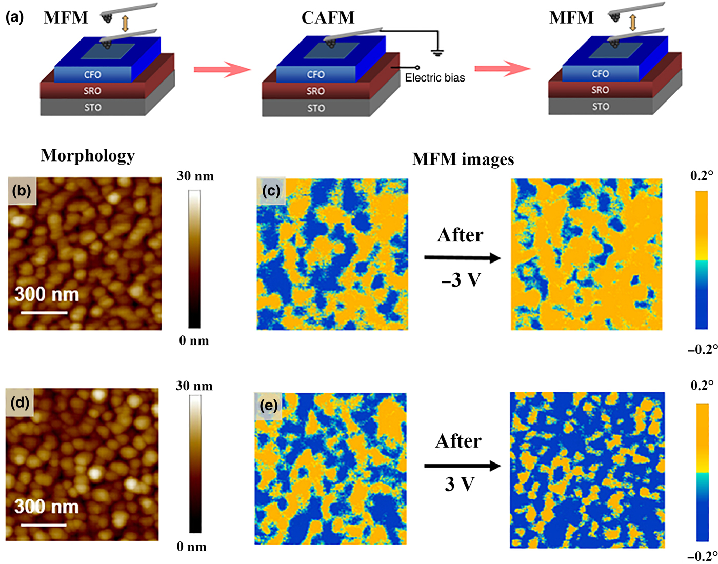
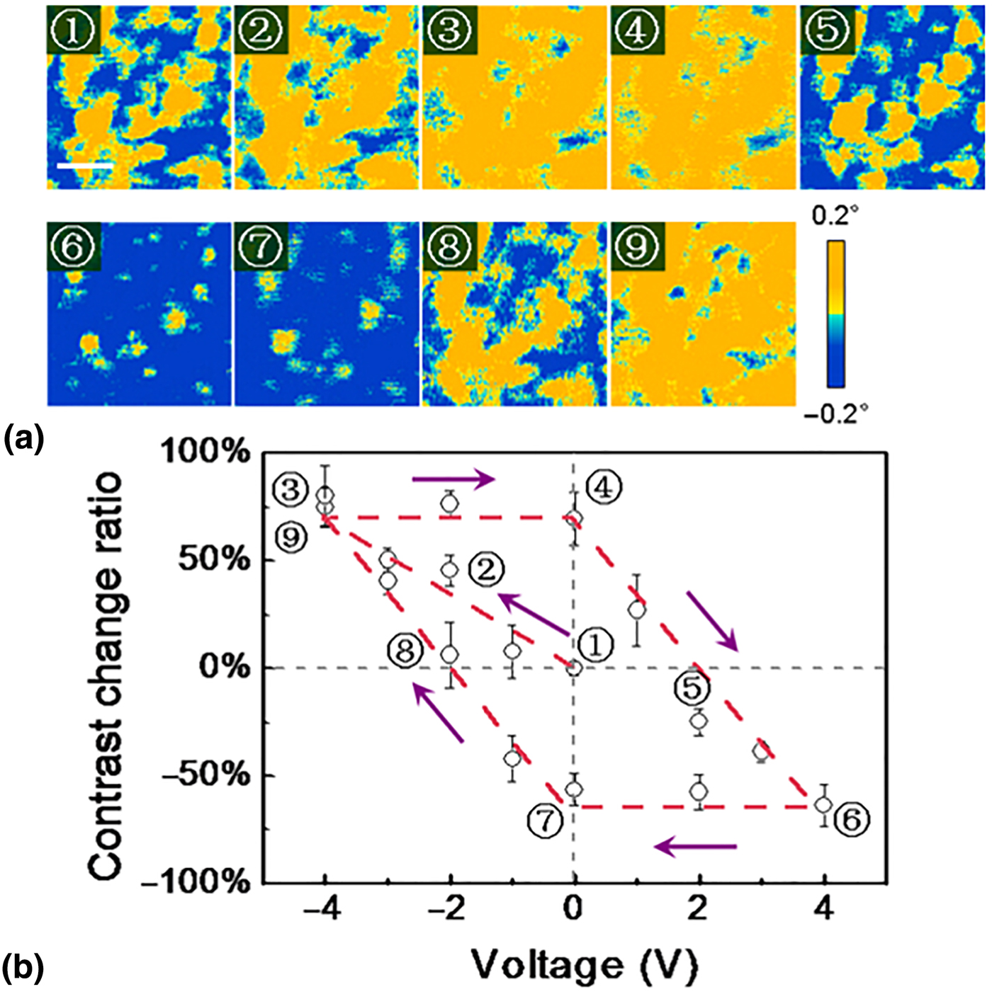
In 2015, Chen et al. investigated nanoscale magnetization reversal through electric field induced local ion migration and redistribution in cobalt ferrite (CFO) thin films via SPM technique for the first time.[Reference Chen, Zhu, Xiao, Liu, Feng, Ding and Li23] The use of C-AFM and magnetic force microscope (MFM) modes allowed them to monitor the dynamic evolution of the conductance and out-of-plane magnetization of CFO, wherein the correlation between them can offer important insights into the underlying mechanism of ion-based magnetization reversal. (110)-textured CFO thin film is prepared by pulse laser deposition (PLD) technique on SrRuO3/SrTiO3 (SRO/STO) substrates, and confirmed by x-ray diffractive pattern with a cubic Fm3m inverse spinel structure. Due to the non-uniform distribution of the ionic species in the plasma glow or the scattering of the ions by the residue gas molecules during PLD preparation, vacancies exist in the as-prepared CFO thin film, which is iron-deficient with the Fe/Co atomic ratio of 1.9 as evidenced by the energy-dispersive x-ray spectrum. As shown in Fig. 1, the magnetic domains with the out-of-plane magnetization point up (in yellow) and down (in blue) are distributed randomly whereas showing almost equal total areas [left panels of Figs. 1(c) and 1(e), respectively]. The application of −3 V voltage to the sample can tune the magnetization direction of most of the domains to pointing upwards [right panel of Fig. 1(c)], while the application of 3 V voltage shows an opposite influence [right panel of Fig. 1(e)]. Upon reversing the magnetization of the Co/Cr coated tip, a mirror image of the right panel of Figs. 1(c) and 1(e) are obtained, respectively. This confirms that the observed changes in the MFM images under the applied electric field are arising from the magnetic rather than electrostatic interactions between the MFM tip and the sample, and preliminarily suggests that nanoscale electric field-induced magnetization inversion can be realized in the CFO thin film at room temperature. Application of external voltages is applied in the sequence of 0 V → −4 V → 0 V → 4 V → 0 V → −4 V reveals that the electric field induced magnetization modulation is completely reversible [Fig. 2(a)]. By defining the contrast change ratio as that between the total areas of the electrically produced upward-magnetized domains and the initially upward-magnetized domains, ~70% modulation of the magnetization in CFO thin films is demonstrated [Fig. 2(b)].
Electric field-induced magnetization reversal in CFO thin films. (a) Schematic illustration of the experimental setups for the C-AFM and MFM measurements. (b), (d) Morphologies of the CFO thin film at the pristine state and (c), (e) corresponding MFM images of the CFO thin film at the pristine state and after being subjected to biased voltages of −3 and 3 V, respectively. Scale bar: 300 nm. Adapted with permission from Ref. Reference Chen, Zhu, Xiao, Liu, Feng, Ding and Li23 (American Chemical Society, 2015).
Reversible magnetization reversal under various electric fields. (a) MFM images of the CFO thin film at the pristine state and after being subjected to various biased voltages. Scale bar: 200 nm. (b) Evolution of the contrast change ratio after being subjected to various biased voltages in the sequence 0 V–4 V–0 V–4 V–0 V–4 V. Adapted with permission from Ref. Reference Chen, Zhu, Xiao, Liu, Feng, Ding and Li23 (American Chemical Society, 2015).
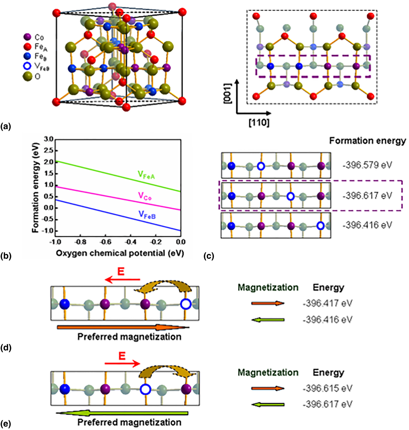
For better understanding the underlying mechanism of the observed magnetization reversal in CFO thin films, first-principles calculations are performed to verify the relationship between the electric field-induced ion migration and the magnetic anisotropy of the CFO unit. As shown in Fig. 3(a), A site of the unit cell is occupied by iron species while the B-site-paired Co2+ and Fe3+ ions are alternatively arranged along the <110> direction in an ideal CoFe2O4. Calculation results suggest that the formation energy of the B-site Fe vacancies is lower than that of the B-site Co vacancies and the A-site Fe vacancies [Fig. 3(b)]. Therefore, B-site Fe vacancies can be more easily formed in the CFO thin films and are consistent with the experimental Fe/Co ratio of 1.9. In the subsequent calculation works, one Fe vacancy is introduced into the CFO unit cell, while the CFO thin film with different Fe/Co ratio will exhibit different magnetic and magnetization modulation behavior. Changing the composition of the CFO thin films can be realized by modifying the deposition condition, e.g., the composition of the PLD target, sputtering angle, chamber pressure, and, etc. It is noteworthy that the B-site Fe vacancy prefers to stay between two Co2+ ions to lower the total energy of the unit cell [Fig. 3(c)]. When an electric field along the [ $\overline {11} $ 0] direction is applied onto the model system, the neighboring Co2+ ion on the right of the Fe vacancy will exchange its occupation with the Fe vacancy, forming a new configuration of Fe3+-Co2+-Co2+-VFeB and a lower total energy of the unit cell with its magnetization pointing along the [110] direction [Fig. 3(d)]. With the shift of the uniaxial magnetic anisotropy of the as-fabricated CFO thin film to a unidirectional one upon being subjected to external electric fields, the magnetization prefers to point along [110] direction. By reversing the polarity of the applied electric field, Co2+ ion will drift back to its original position and the energetically preferred magnetization is aligned along the [ $\overline {11} $ 0] direction [Fig. 3(e)]. As such, it is confirmed that the electric field-induced migration and local redistribution of Co2+ ions account for the magnetization reversal in CFO thin films. The back-diffusion energy barrier for Co2+ cation is ~0.6 eV, which is sufficient to overcome the thermal disturbance at room temperature and make the system stable. As such, the ion migration process is nonvolatile in nature, and the retention of magnetization reversal can be sustained for days. It is noteworthy that the local redistribution of Co2+ ions may also result in dielectric polarization, which may influence the magnetization reversal via a multiferroic coupling.
Theoretical model for the electric field-induced magnetization reversal in a CFO unit cell. (a) Lattice structure of an ideal CoFe2O4 unit cell (left panel) and the corresponding (110) plane (right panel). The dashed box marks the distribution of the cations along the [110] direction. (b) Dependence of the formation energy of the Co vacancy, A-site Fe vacancy, and B-site Fe vacancy on the oxygen chemical potential. (c) Localized structures of the CFO unit cell with different locations of the Fe vacancy occupation. (d), (e) Localized structures and preferred magnetizations of the CFO unit cell with a Fe vacancy present along the [110] direction and with different locations of the Co occupation after the occurrence of electric field-induced migration of Co2+ ions. The shaded brown spheres represent oxygen atoms located outside the [110] crystal plane under evaluation. Reproduced with permission from Ref. Reference Chen, Zhu, Xiao, Liu, Feng, Ding and Li23. (American Chemical Society, 2015).
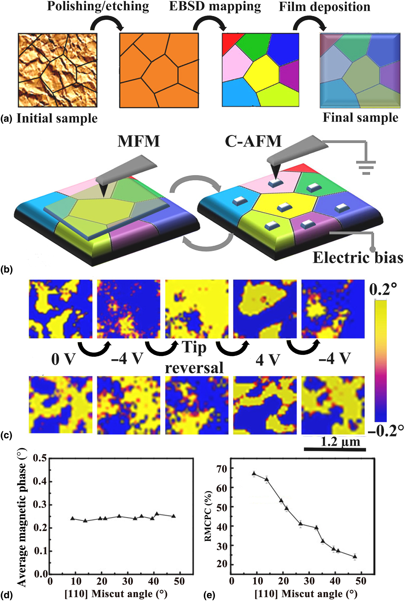
The modulation of magnetism with the electric field-induced ion migration within the magnetic structure provides the advantage of being simple and stable for large numbers of device operating cycles. The crystalline direction of the ferrite film may also strongly influence the magnetization modulation as different crystal directions can have different extents of cation migration and redistribution.[Reference Waser, Dittmann, Staikov and Szot35, Reference Zhang, Schultz, Li, Chien, Salvador and Rohrer36] To evaluate the efficiency of ion migration and related magnetism modulation along various crystalline direction, epitaxial polycrystalline CFO sample with symmetries and orientations repeating the underneath polycrystalline SRO substrate (with a span of low to high index [hkl] crystal directions) is deposited in a grain over grain (cube-on-cube) combinatorial substrate epitaxy (CSE) fashion by PLD technique [Fig. 4(a)],[Reference Dhanapal, Guo, Wang and Li37] which exhibits magnetization reversal behavior as shown in Figs. 4(b) and 4(c). CSE approach further confirms that although the magnetization reversal in all miscut angles from [110] direction are fully reversible, obvious decrease in the remanent magnetic contrast phase change ratio upon being subjected to either +4 V or −4 V stimuli is recorded as the miscut angle increases gradually [Figs. 4(d) and 4(e)]. The maximum magnetization modulation along [110] direction is consistent with the relative ease of Co2+ ion migration between the B-site Fe3+ vacancies along the B–B axis.
(a) Schematic of the Combinatorial Substrate Epitaxy (CSE) approach to derive the structure-property relationship at the grain scale: (1) Rough polycrystalline surface; (2) topography image of the polished surface; (3) the orientation of the substrate grains determined by Electron Backscattered Diffraction (EBSD); and (4) EBSD/Energy-dispersive x-ray spectroscopy mapping and scanning probe microscopy performed over the same region of the polycrystalline substrate after film deposition to determine the library of the structure-property relationship. (b) Illustration of MFM and C-AFM operations on the CSE samples. (c) Electric field-induced magnetization reversal on domains with the miscut angle from the [110] direction of 8.9° (upper panel) and 36.6° (lower panel), respectively. (d) Average magnetic phase of the domains after being subjected to 0 V–4 V – + 4 V voltage cycles, as a function of the miscut angle from the [110] direction. (e) Average reversible magnetic contrast phase change (RMCPC) upon being subjected to either + 4 V or −4 V stimuli, as a function of the miscut angle from the [110] direction. Reproduced with permission from Ref. Reference Dhanapal, Guo, Wang and Li37 under the Creative Commons Attribution (CC BY) license (http://creativecommons.org/licenses/by/4.0/).
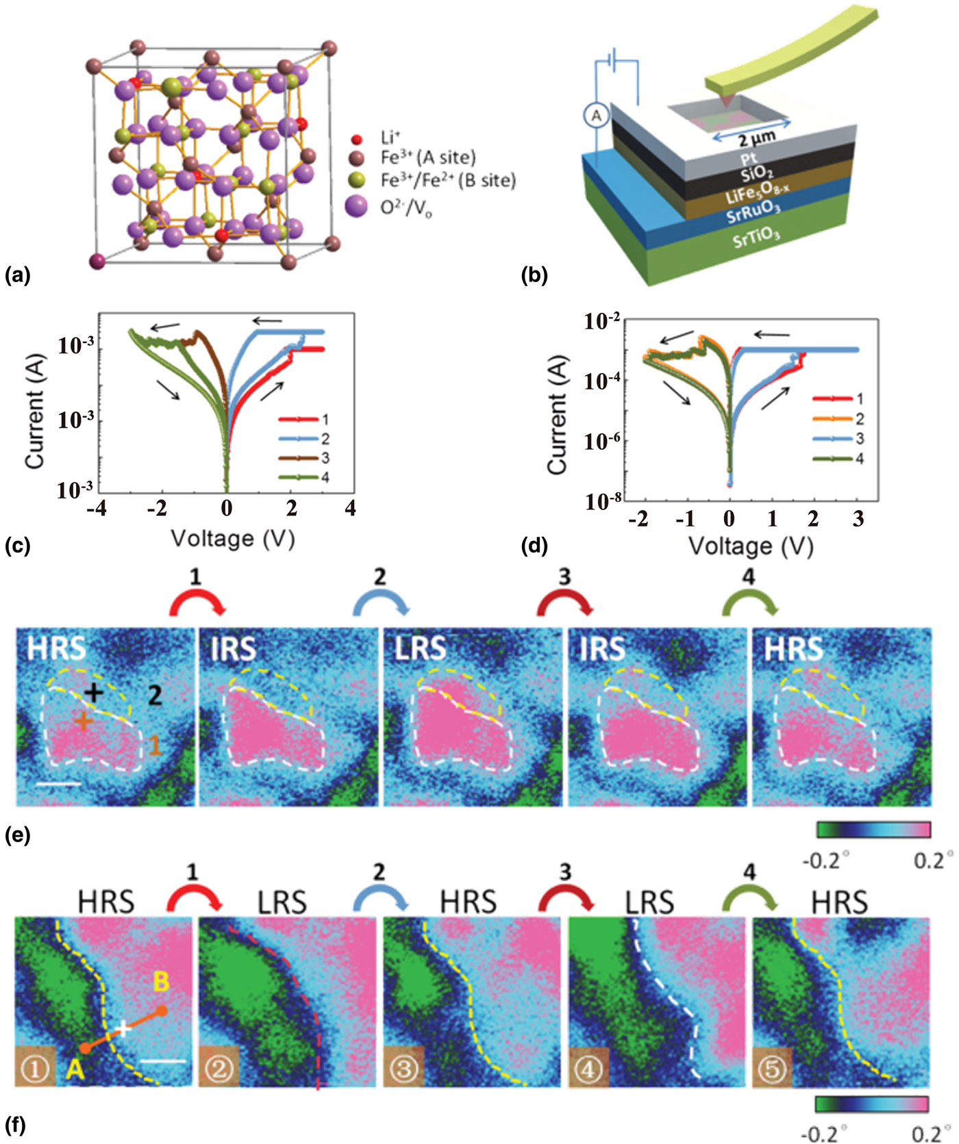
In order to explore the spatial uniformity of magnetization modulation via ion migration, Zhu et al. further correlate the observed magnetic behavior with electrical characteristics in lithium ferrite LiFe5O8 (LFO) thin films. LFO is also a fast ion conductor, wherein the migration of Li+ ions may lead to localized resistive switching and helps understand the mechanism of magnetization modulation. In LiFe5O8, the Li+ ions and three-fifths of the Fe3+ ions occupy the B-site octahedral center, while the remaining Fe3+ ions occupy the center of the A site tetrahedron [Fig. 5(a)].[Reference Zhu, Zhou, Chen, Guo, Liu, Li and Lu24] A and B-site Fe3+ ions are antiferromagnetically coupled. In oxygen deficient LiFe5O8−x samples part of the B-site Fe3+ ions are reduced to Fe2+ ions with the lower magnetic moment, and the net magnetic moment of the sample is determined by the difference of the A and B-site occupied Fe3+ ions. De-intercalation of Li+ ion out of the host LFM material can result in re-oxidation of Fe2+ to Fe3+ ions, hence increasing the magnetic moment of the lithium ferrite correspondingly. The reverse process occurs during Li+ ion intercalation. Meanwhile, the Li+ ion de-intercalation/intercalation process modulates the local concentration of hopping centers such as Li+ vacancies in the film, which in turn can lead to resistive switching between the initial high resistance state (HRS) and low resistance state (LRS). In accordance with this hypothesis, the oxygen-deficient LiFe5O8−x layer sandwiched between SRO and Pt electrodes [Fig. 5(b)] exhibits three level resistive switching feature [Fig. 5(c)] and a continuous modulation of the upward-magnetized domain [Fig. 5(e)]. The dimension of the magnetic domain increases and decreases at the LRS and HRS of the resistive switching process, correspondingly, while the magnitude of the magnetization modulation is not spatially uniform, confirming that the observed magnetization reversal is ascribed to the conductive filaments growth and annihilation associated with the localized migration of Li+ ion and the subsequent redox activities. Detailed analysis of the MFM image evolution also suggests that local modulation provided by Li+ ion de-intercalation and intercalation lead to the local domain wall movement within a distance of 100 nm [Figs. 5(d) and 5(f)], which can be ascribed to the dimension increase/decrease of the domains with the magnetization direction point upwards or downwards, respectively. The overall volume change of the material and related strain effects caused by the extraction and intercalation of Li+ ions from and into the LFO grains may also influence the magnetization of the sample.
Reversible modulation of magnetic domain properties in Pt/LFO/SRO devices. (a) The inverse spinel-structured LiFe5O8 unit cell. (b) Schematic of the measurement setup. After programming the Pt/LFO/SRO device (defined by the via structure), the MFM images were obtained without the bias voltage. (c) and (d) current-voltage characteristics of the Pt/LFO/SRO device showing consecutive and bistable resistive switching behaviors, respectively. (e) MFM images of an area with a dominant upward domain at different resistance states in (c). Scale bar: 200 nm. (f) MFM images of an area with apparent magnetization changes, measured at different resistance states in (d). Scale bar: 200 nm. Reproduced with permission from Ref. Reference Zhu, Zhou, Chen, Guo, Liu, Li and Lu24 (John Wiley and Sons, 2016).
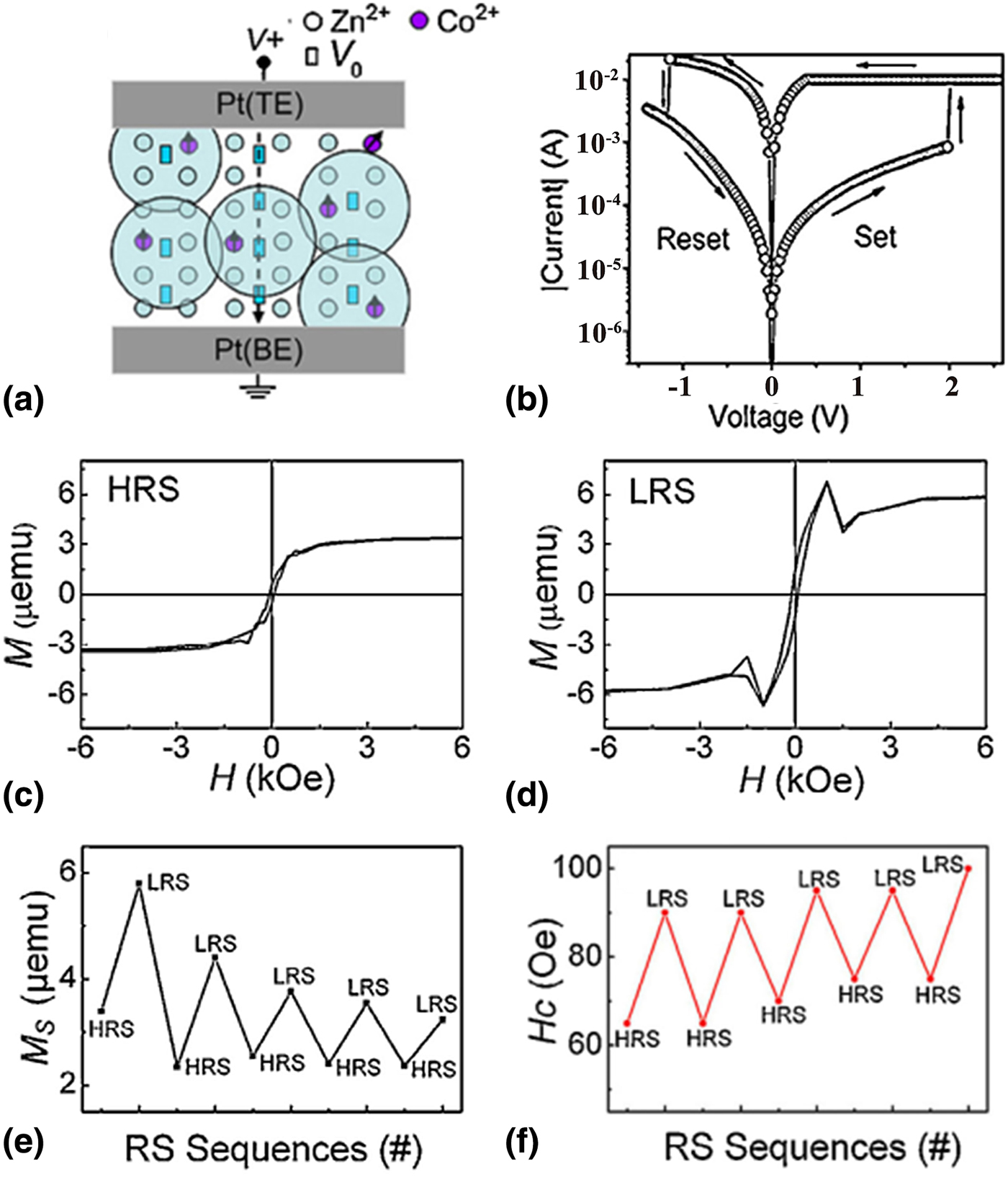
The ion migration-based magnetization modulation is also reflected in the changes of the saturated magnetic moment (M S) and coercive field (H C) of magnetic thin film.[Reference Chen, Song, Chen, Gao, Zeng and Pan25, Reference Ohno, Chiba, Matsukura, Omiya, Abe, Dietl, Ohno and Ohtani38–Reference Stolichnov, Riester, Trodahl, Setter, Rushforth, Edmonds, Campion, Foxon, Gallagher and Jungwirth40] Song et al. investigated the resistive switching and magnetic modulation in dilute magnetic semiconductors (DMS) Zn0.95Co0.05O. It is found that the migration of oxygen ions and formation of oxygen vacancy conductive filaments yields a greater overall volume occupied by the bound magnetic polarons [Fig. 6(a)], which increases the probability of overlapping more Co2+ ions into the ferromagnetic domain and thus enhances the ferromagnetism of the DMS layer. As shown in Figs. 6(b)–6(f), accompanying the resistive switching between the HRS and LRS, both the saturated magnetization (M S) and the coercive field (H C) of the Zn0.95Co0.05O layer are greatly influenced reversibly, confirming the occurrence of ion migration induced magnetism modulation. As such, manipulating the magnetization in an electrical means without the need of external magnetic field can be used to achieve a new paradigm where the interaction of spin and charge lead to faster, low-energy, and multibit information storage applications. The utilization of ionic liquid as the gating medium further enhances the efficiency of electric field-induced modulation on complex oxide materials of LaxSr1−xMnO, which shows tunable Curie temperature, enhanced saturation magnetization and obvious changes in the electrical resistance.[Reference Cui, Song, Wang, Yan, Peng, Miao, Mao, Li, Chen, Feng and Pan26, Reference Cui, Song, Gehring, Li, Wang, Chen, Peng, Mao, Zeng and Pan27, Reference Chiba41–Reference Zhang, Yin, Wang, Bin, Feng and Cheng45]
(a) Mechanism of the resistive switching and magnetic modulation during the set process and (b) the current-voltage curve of the Pt/Zn0.95Co0.05O/Pt device. The oxygen vacancy-based conductive filament is highlighted by the vertical arrow in (a). Room-temperature magnetization hysteresis loops of the Pt/Zn0.95Co0.05O/Pt device at (c) HRS and (d) LRS. The (e) saturated magnetic moment (M S) and (f) coercive field (H c) are modulated reversibly during the resistive switching process. Reproduced with permission from Ref. Reference Chen, Song, Chen, Gao, Zeng and Pan25 (John Wiley and Sons, 2012).
Reversible control of magnetism by external ion modulation
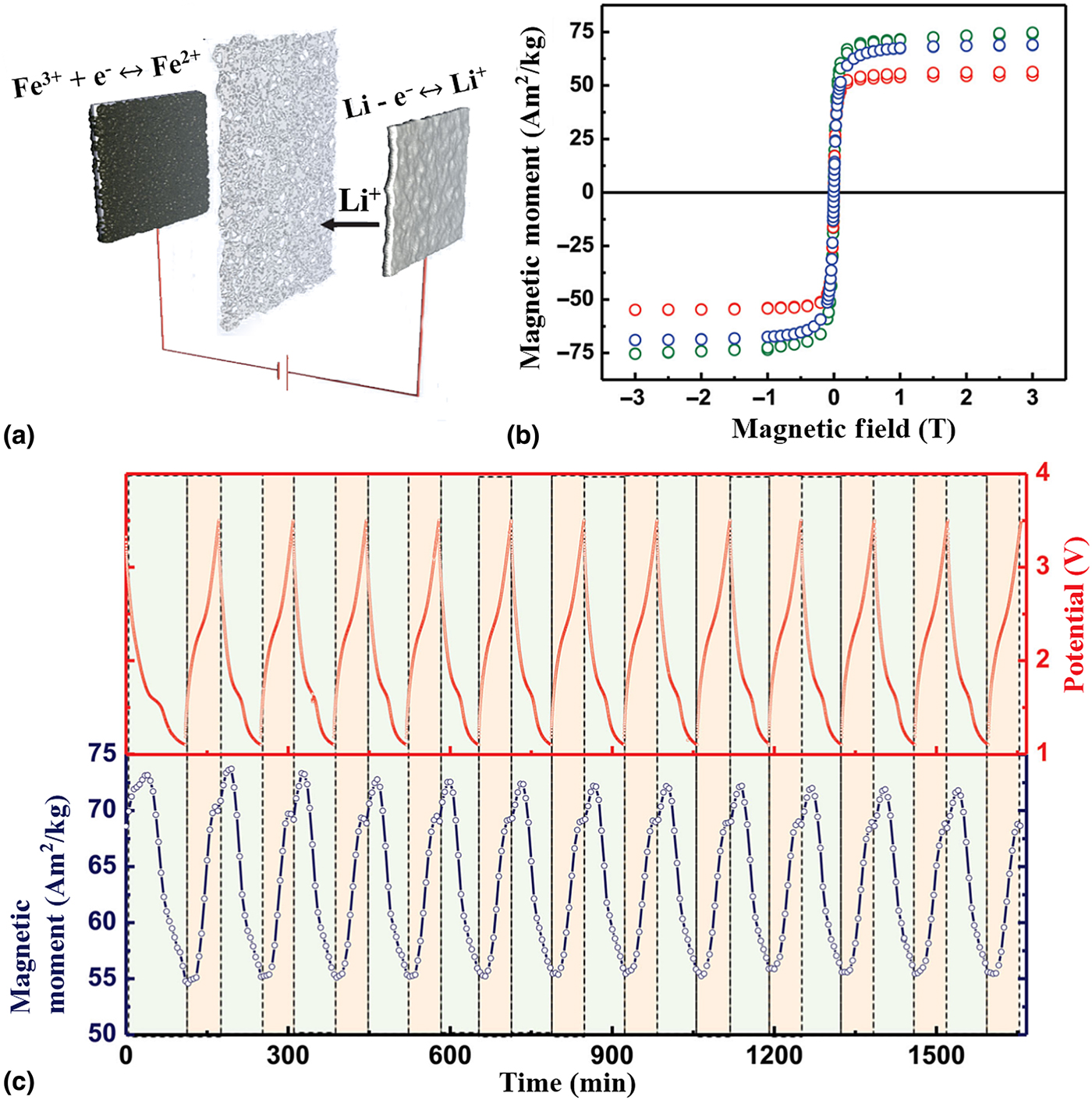
In addition to the migration of ionic species that forms the magnetic structures, the ions from the external sources may also influence the magnetism of ferromagnetic and antiferromagnetic materials.[Reference Dasgupta, Das, Knapp, Brand, Ehrenberg, Kruk and Hahn21, Reference Bauer, Yao, Tan, Agrawal, Emori, Tuller, Dijken and Beach22, Reference Cui, Song, Wang, Yan, Peng, Miao, Mao, Li, Chen, Feng and Pan26, Reference Cui, Song, Gehring, Li, Wang, Chen, Peng, Mao, Zeng and Pan27] For instance, due to the successful demonstration of reversible lithium ion intercalation process for thousands of charge-discharge cycles in electrochemical systems,[Reference Zhu, Liu, Zhuang, Wang, Wang and Xia46, Reference Sun, Rajasekhara, Goodenough and Zhou47] Dasgupta et al. established a chemistry-controlled yet fully reversible change in magnetic response of the spinel iron oxide γ-Fe2O3 to the Li+ ion intercalation and de-intercalation processes, with LiPF6 as the external ion source in liquid state.[Reference Dasgupta, Das, Knapp, Brand, Ehrenberg, Kruk and Hahn21] It is shown that by carefully selecting the discharge potential, up to 1 mole Li+ ion per formula unit of γ-Fe2O3 can be inserted into the iron ferrite crystal [Fig. 7(a)], which leads to large switching between distinctly different magnetic states while maintains the spinel structure intact [Fig. 7(b)]. The Li intercalation-induced magnetization modulation shows two clearly discernible regimes [Fig. 7(c)]. At the initial state when the discharge potential decreases from 3.5 to 1.7 V, the magnetization M S rises slightly. Then a monotonic and significant decrease in M S from 74 to 54 Am2/kg is observed. This can be ascribed to the insertion of Li+ ions that reduce part of the tetrahedral Fe3+ to Fe2+ species and their subsequent rearrangement to the neighboring octahedral site with more space. Net ferromagnetism increases as the B sublattice occupancy grows at the expense of A sublattice shrinkage. The change in the magnetization is fully reversible as shown in the charge-discharge cycles of Fig. 7(c). In principle, the concept of dynamic and reversible control over bulk magnetism via ion migration and electrochemical processes can be applied to any intercalation-friendly magnetic materials.
(a) Schematic of the typical electrochemical cell showing reversible Li+ ion intercalation and de-intercalation with spinel iron ferrite γ-Fe2O3. (b) Magnetic hysteresis measured at different stages of lithiation: blue, green, and red symbols stand for the as-prepared γ-Fe2O3 sample, and the samples that are discharged down to 1.7 and 1.1 V, respectively. after reaching the desired discharge potential, the electrochemical cell has been electrically disconnected prior to the magnetic measurements. (c) Fully-reversible variation in magnetic response (measured at the magnetic field of 1 T) of the sample. The discharge and charge cycles are carried out with a potentiometric constant current pf 115 mA/g and cut-off potentials of 1.1 and 3.5 V versus Li+/Li during lithiation and delithiation steps, respectively. Reproduced with permission from Ref. Reference Dasgupta, Das, Knapp, Brand, Ehrenberg, Kruk and Hahn21 (John Wiley and Sons, 2014).
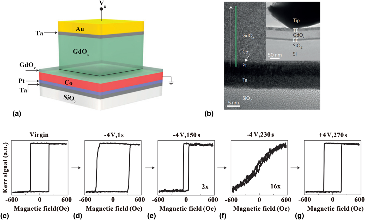
On the other hand, it is known that ferromagnetic bilayers such as Co/AlOx and CoFe/MgO exhibit strong perpendicular magnetic anisotropy (PMA) as derived from interfacial Co/O interaction.[Reference Manchon, Pizzini, Vogel, Uhlîr, Lombard, Ducruet, Auffret, Rodmacq, Dieny, Hochstrasser and Panaccione48, Reference Rodmacq, Manchon, Ducruet, Auffret and Dieny49] Rather than the charge accumulation and band shifting in the metal layer,[Reference Maruyama, Shiota, Nozaki, Ohta, Toda, Mizuguchi, Tulapurkar, Shinjo, Shiraishi, Mizukami, Ando and Suzuki10, Reference Shiota, Nozaki, Bonell, Murakami, Shinjo and Suzuki50, Reference Wang, Li, Hageman and Chien51] modification to the oxygen stoichiometry and defect structure at the metal/metal oxide interface via electric field-driven oxygen ion migration can also tune the magnetism of the magnetic metal thin film reversibly.[Reference Bauer, Yao, Tan, Agrawal, Emori, Tuller, Dijken and Beach22] Bauer et al. studied the interfacial magnetism modulation of Co/GdOx bilayer in a Au/Ta/GdOx/Co/Pt/Ta stacking structure [Figs. 8(a) and 8(b)] associated with the occurrence of electric field-induced migration of the oxygen ion from the metal oxide layer to the metal thin film. Scanning magneto-optical Kerr (MOKE) analysis reveals that the application of −4 V voltage for 240 s at elevated temperature of 100 °C give rise to an obvious and progressive decrease in the coercive field beneath the electrode, which can be ascribed to the over-oxidation of the Co interface and the reduction in PMA [Figs. 8(c)–8(f)]. It is noteworthy that the enhanced PMA as shown in Fig. 8(d) may also be arising from the better interaction between the Co and Pt at their interface. The PMA is completely recovered by reversing the polarity of the gating voltage to +4 V at 100 °C for 270 s [Fig. 8(g)], allowing the voltage control of magnetism to an extent that has never before been achieved with conventional magneto-electric coupling mechanisms.
(a) Device schematic and (b) high-resolution cross-sectional transmission electron microscopic image of the Au/Ta/GdOx/Co/Pt/Ta multilayer structure for the electric field-controlled magnetic anisotropy. Polar magneto-optical Kerr (MOKE) hysteresis loops of the sample measured at room temperature at the centre of the gate electrode showing the device in its virgin state (c), after applying V g = −4 V at 100 °C for (d) 1 s, (e) 150 s and (f) 230 s, and (g) after applying V g = 4 V at 100 °C for 270 s. Note that the Kerr signal intensity in (e) is reduced by a factor of 2 and in (f) by a factor of 16, as indicated by inset number. Reproduced with permission from Ref. Reference Bauer, Yao, Tan, Agrawal, Emori, Tuller, Dijken and Beach22 (Springer Nature, 2014).
Construction of magnetic conductive filaments via foreign metal ion migration and redox activities
The key feature of nanoscale ion migration and related redox activities are the construction of discrete conductive filaments in resistive switching memory, which give rise to the bistable information storage and even in-memory computing capabilities.[Reference Maier14–Reference Yang, Strukov and Stewart16] Generally, electrochemically active electrode metals (including Ag, Cu, Co, Ni, and, etc.) will be oxidized into cations under the application of the external electric field, and subsequently injected into the insulating layer. The cations will migrate towards the cathode through the insulating media, and get reduced to metal atoms with electrons injected from the cathode. The reduction of the cations to atoms can occur either at the insulator/cathode interface or inside the insulating later, which depends on the difference in the motilities of the cations and electrons in the insulator. The aggregation of the reduced metal atoms and continuous growth of the metal cluster will eventually form a conical shaped conductive filament that connects both the anode and cathode, leading to obvious resistance/conductance switching of the sandwich structure devices to the LRS. When the polarity of the external electric field is reversed, the conductive filament will be disrupted at its narrowest point through either Joule heating induced melting or electrochemical oxidation of the metal atoms into the cations, programming the device back to the initial HRS. Particularly, the formation and evolution of magnetic conductive filaments by the injection and migration of magnetic ions e.g., Co2+ and Ni2+ would also endow resistive switching devices more interesting magneto-ionic characteristics that supplement the modulation of magnetic properties as discussed above. For example, if the conductive filament in a ferromagnet/insulator/ferromagnet device is not connected to the cathode and the effective thickness of the residual insulating layer is thin enough for the spin-polarized tunneling of electrons across it, a magnetic tunnel junction (MJT) with a TMR phenomena would be theoretically observed.[Reference Miyazaki and Tezuka52–Reference Yuasa, Nagahama, Fukushima, Suzuki and Ando55]
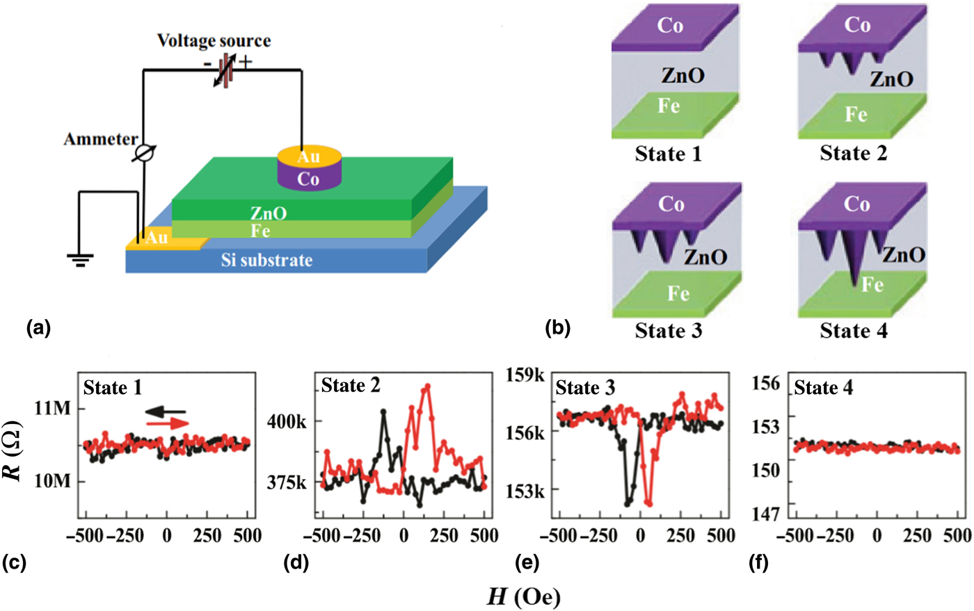
In 2014, Yang et al. for the first time report the construction of MTJ by the migration of Co2+ ions in Co/ZnO/Fe sandwich structures.[Reference Yang, Zhan, Zhu, Liu, Yang, Hu, Shang, Pan, Chen and Li28] As shown in Fig. 9(a), multi-layered films with a structure of Au/Co/ZnO/Fe/Au are deposited on thermally oxidized silicon substrates. The application of positively biased voltage sweep can ionize the top cobalt electrode and inject the Co2+ ions into the ZnO layer. After traveling a short distance within the insulating layer, the cations are reduced back to atomic forms and gradually from the metallic Co conductive filaments from the anode to the cathode [Fig. 9(b)]. By readily controlling the gap width between the magnetic conductive filament front and the bottom ferromagnetic electrodes for the spin-polarized tunneling of conduction electrons (length of the Co filament), the resistive switching device exhibits non TMR, positive TMR with the Co filament, and the Fe electrode in an anti-parallel magnetic configuration under low magnetic field, negative TMR arising from the resonant tunneling caused by impurity scattering in the ZnO barrier,[Reference Jeong, Thomas, Katiyar, Scott, Kohlstedt, Petraru and Hwang56] and non TMR phenomena in its HRS, intermediate resistance states, and LRS, respectively [Figs. 9(c)–9(f)]. In addition to the magnetization modulation with the native ions presenting in the ferrite thin films, the construction of magnetic tunneling junction and related TMR phenomena through ion migration in resistive switching cells with ferromagnetic electrodes may provide a more versatile platform for building novel sensors and information storage devices. Nevertheless, it is noteworthy that oxidization of the magnetic metal (such as Co or Fe) electrodes may also lead to the modification to the oxygen stoichiometry and defect structure at the metal/metal oxide interface, which tunes the magnetism of the magnetic metal thin film reversibly.
(a) Schematic of the multi-layered resistive switching Co/ZnO/Fe structures. (b) Evolutional formation of the Co conductive filament in the Co/ZnO/Fe structure under the positively biased voltage applied to the top cobalt electrode. The tunneling magnetoresistance (TMR) of the CoZnO/Fe structures measured in (c) State 1, (d) State 2, (e) State 3 and (f) State 4. Reproduced with permission from Ref. Reference Yang, Zhan, Zhu, Liu, Yang, Hu, Shang, Pan, Chen and Li28 (Institute of Physics (IOP), 2014).
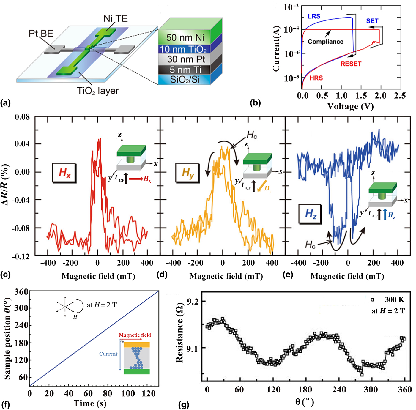
Inspired by the above work, Otsuka and Long et al. constructed ferromagnetic conductive filaments in resistive switching devices with Co2+ or Ni2+ ions, and explored the AMR behavior of the Ni/TiO2/Pt or Co/HfO2/Pt structure in their LRS [Figs. 10(a) and 10(b)].[Reference Otsuka, Hamada, Shimizu and Shingubara29–Reference Li, Liu, Teng, Long, Guo, Zhang, Wu, Yu, Liu, Lv and Liu31] It is found that the Ni/TiO2/Pt device shows convexity in its AMR plot when the direction of the magnetic field is perpendicular to the direction electric current flowing across the device [Figs. 10(c) and 10(d)], whereas a concavity is observed when the magnetic field is aligned in the direction parallel to that of the device currents [Fig. 10(e)].[Reference Otsuka, Hamada, Shimizu and Shingubara29, Reference Otsuka, Hamada, Ito, Shimizu and Shingubara30] This is consistent with the fact that AMR occurred in ferromagnetic transition metal depends strongly on the direction of the magnetization with respect to the electric current direction.[Reference Smit57, Reference McGuire and Potter58] By rotating the direction of the out-of-plane magnetic field with respect to the substrate surface with a fixed magnitude of 2 T in the LRS of the Co/HfO2/Pt device [Fig. 10(f)], it is demonstrated that the spontaneous magnetization of the electroformed Co conductive filament, showing maximum magnetoresistance in the resistance-rotating angle curve [Fig. 10(g)], is tilted by 30° from the device current direction. As such, the construction of ferromagnetic conductive filaments with clear magnetic structures is not only beneficial for making a multilevel memory with both resistive switching and spin dependences but also useful to reveal their detailed magnetic structure information.
(a) Schematics and cross-section of the crossbar Ni/TiO2/Pt device structure. (b) The typical current-voltage curve of the Ni/TiO2/Pt device showing unipolar resistive switching characteristics. Anisotropic characteristics of the LRS Ni/TiO2/Pt device with the external magnetic field applied in the directions of (c) H x, (d) H y and (e) H z, respectively. (f) Scanning of the out-of-plane magnetic field direction with respect to the substrate surface and (g) the related room-temperature magnetoresistance of the Co /HfO2/Pt device as a function of the rotating angle. (a)–(e) are reproduced with permission from Ref. Reference Otsuka, Hamada, Shimizu and Shingubara29 (Springer Nature, 2014). (f) and (g) are reproduced with permission from Ref. Reference Li, Liu, Teng, Long, Guo, Zhang, Wu, Yu, Liu, Lv and Liu31 under the Creative Commons Attribution (CC BY) license (http://creativecommons.org/licenses/by/4.0/).
Conclusion and future outlook
The electric field-induced ion migration in resistive switching devices provides a simple yet versatile approach for modulating the magnetism of the functional materials. Migration of ionic specie that either constitutes the magnetic structure or comes from the external sources can effectively lead to the magnetization modulation in ferromagnetic thin films, which is useful for realizing low power spintronic devices.[Reference Bi, Sun and Xu69] The construction of foreign magnetic conductive filaments in the insulating matrix also gives rise to TMR and AMR characteristics. Recently it is demonstrated that by accurately controlling the evolution dynamics and thus the dimension of the conductive filaments, NPC with quantized conductance characteristics can be obtained in resistive switching devices. The stepwise development of the device conductance in the unit of G 0 = 77.5 uS greatly decorates the bistable switching features of memory devices, and allows for the bottom-up design of quantum information processing and neuromorphic computing architectures through the higher-logic algorithm.[Reference Hasegawa, Terabe, Tsuruoka and Aono59–Reference Krishnan, Muruganathan and Tsuruoka65] On the other hand, the ballistic magnetoresistance effect discovered in 1999 significantly stimulates the upsurge of research on the submicron ferromagnetic nanostructure.[Reference Garcia, Munoz and Zhao66–Reference Tatara, Zhao, Munoz and García68] In case that this anomalous giant magnetoresistance effect can be reproduced precisely in the quantized conductance states of the magnetic NPC formed by Co2+ or Ni2+ migration in resistive switching memories, integration of multiple functions such as sensing, data processing, and storage into a single cell may be realized for the settlement of the von Neumann bottleneck issue encountered by the modern computer systems.
Acknowledgments
The authors acknowledge the financial support from the National Key R&D Program of China (2017YFB0405604 and 2016YFA0201102), the National Natural Science Foundation of China (61722407, 61674153, 51525103, 61704178, 11474295, and 51472210), China Postdoctoral Science Foundation (2016LH0050 and 2017M610379), K. C. Wong Education Foundation (rczx0800), the Natural Science Foundation of Zhejiang Province (LR17E020001), the Provincial Natural Science Foundation of Hunan (2018JJ4037), Ningbo Science and Technology Innovation Team (2015B11001), and Key Laboratory of Advanced Materials of Ministry of Education (2017AML04).


