


Introduction
Optoelectronic properties of transition metal dichalcogenides (TMDs) can be manipulated by taking the system out of equilibrium, which has been done using temperature [Reference Molina-Sánchez, Palummo, Marini and Wirtz1, Reference Hu, Zhang, Titze, Deng, Li and Cheng2, Reference Yin, Wang, Cao, Tang, Luo, Zheng, Wong, Wang, Quek, Zhang, Rusydi and Wee3, Reference Tongay, Suh, Ataca, Fan, Luce, Kang, Liu, Ko, Raghunathanan, Zhou, Ogletree, Li, Grossman and Wu4], pressure [Reference Nayak, Bhattacharyya, Zhu, Liu, Wu, Pandey, Jin, Singh, Akinwande and Lin5, Reference Dou, Ding, Jiang and Sun6], electrical bias [Reference Sanchez, Ovchinnikov, Misra, Allain and Kis7, Reference Ross, Wu, Yu, Ghimire, Jones, Aivazian, Yan, Mandrus, Xiao, Yao and Xu8], magnetic fields [Reference Stier, McCreary, Jonker, Kono and Crooker9], and light ion [Reference Wang, Yang, Chen, Mann, Bushmaker and Cronin10, Reference Shin, Cho, Kim, Pak, Kim, Lee, Kim, Chung, Hong and Lee11, Reference Vogl, Sripathy, Sharma, Reddy, Sullivan, Machacek, Zhang, Karouta, Buchler, Doherty, Lu and Lam12] and electron irradiations [Reference Vogl, Sripathy, Sharma, Reddy, Sullivan, Machacek, Zhang, Karouta, Buchler, Doherty, Lu and Lam12, Reference Parkin, Balan, Liang, Das, Lamparski, Naylor, Rodríguez-Manzo, Charlie Johnson, Meunier and Drndić13]. Molybdenum disulfide (MoS2) remains the most widely studied TMD material system because of its remarkable flexibility [Reference Singh, Singh, Kim, Yeom and Nalwa14] and enhanced photoresponsivity [Reference Lopez-Sanchez, Lembke, Kayci, Radenovic and Kis15]. Fabrication of MoS2 by chemical vapor deposition (CVD), mechanical exfoliation, and physical vapor deposition introduces intrinsic defects, which has been shown to degrade material's properties [Reference Hong, Hu, Probert, Li, Lv, Yang, Gu, Mao, Feng, Xie, Zhang, Wu, Zhang, Jin, Ji, Zhang, Yuan and Zhang16]. Carbon and oxygen impurities introduced at various stages of fabrication can occupy interstitial sites in MoS2 [Reference Addou, McDonnell, Barrera, Guo, Azcatl, Wang, Zhu, Hinkle, Quevedo-Lopez, Alshareef, Colombo, Hsu and Wallace17], act as traps for charge carriers [Reference Ma and Jena18], and degrade carrier concentrations [Reference Cai, Zhou, Zhang and Zhang19].
Theory, on the other hand, predicts that defects can be used to control properties of single- and multi-layered materials. According to first principles calculations, native defects such as S and Mo vacancies create impurity levels in bulk MoS2 within the band gap and in the valence band and lead to pronounced photon absorption in visible light region [Reference Kumar Saha and Yoshiya20]. These impurity levels can be used to manipulate photovoltaic energy conversion at longer wavelength [Reference Kumar Saha and Yoshiya20]. Several groups investigated the role defects (mostly vacancies and grain boundaries) play in determining the electronic, optical, and optoelectronic properties of low-dimensional MoS2 systems, but no explicit understanding of the phenomena has been attained [Reference Hong, Hu, Probert, Li, Lv, Yang, Gu, Mao, Feng, Xie, Zhang, Wu, Zhang, Jin, Ji, Zhang, Yuan and Zhang16, Reference Kumar Saha and Yoshiya20, Reference Yu, Pan, Shen, Wang, Ong, Xu, Xin, Pan, Wang, Sun, Wang, Zhang, Zhang, Shi and Wang21, Reference Zhou, Zou, Najmaei, Liu, Shi, Kong, Lou, Ajayan, Yakobson and Idrobo22, Reference Haldar, Vovusha, Yadav, Eriksson and Sanyal23, Reference Komsa and Krasheninnikov24]. Most studies focused on doping MoS2 to achieve control of the optical properties, which included studies on chemical doping [Reference Mouri, Miyachi and Matsuda25] and low-energy ion implantation [Reference Nipane, Karmakar, Kaushik, Karande and Lodha26].
Instead of concentrating on low-energy ion implantation, we explore intermediate energy ion irradiation to control defect densities in MoS2. Although low-energy (typically <1 keV) ion implantation provides an exciting route to alter material properties, nuclear energy deposition induces defects that can dominate the material response. In the case of intermediate energies (range from a few hundred keV to several MeV), electronic energy deposition starts to play an important role in the modification of optical properties of these low-dimensional materials. We use ion irradiation to controllably introduce defects and investigate the change in photoluminescence (PL) spectra of MoS2 and elucidate the role defects play in controlling the optical response of the material.
Results and discussion
Photoexcitation in semiconducting MoS2 is expected to produce pairs of bound electrons and holes known as excitons, the recombination of which emits a photon observed as PL. Photogenerated electron–hole pairs can have strong Coulomb interaction, leading to the formation of bound excitons, and can alter the optical transitions in these systems. The spatial confinement combined with the reduced dielectric screening as compared with bulk crystals suggests that the optical response of low-dimensional MoS2 flakes will be dominated by neutral excitons.
Previous studies [Reference Mak, He, Shan and Heinz27, Reference Mak, He, Lee, Lee, Hone, Heinz and Shan28, Reference Wang, Bouet, Lagarde, Vidal, Balocchi, Amand, Marie and Urbaszek29] indicated that the spectrum of bare MoS2 should display two distinctive peaks: A1s exciton peak between 1.86 and 1.92 eV and B1s exciton peak within the range of 2.0–2.1 eV, which are associated with direct optical transitions to the lowest conduction bands from the highest spin-orbit valence bands [Reference Sim, Park, Song, In, Lee, Kim and Choi30, Reference McCreary, Hanbicki, Sivaram and Jonker31, Reference Niehues, Blob, Stiehm, Vasconcellos and Bratschitsch32]. It should be noted that both A1s and B1s exciton peaks are formed by an electron and a hole in the valence band. The ground state A1s exciton has a smaller PL energy than the B1s exciton, which is associated with the spin orbit split valence band. Other possible spectral features in MoS2 include the A− trion peak arising from interactions between two electrons and a hole that can occur when excess electrons bind to photoexcited electron–hole pairs and create positively charged states [Reference Mak, He, Lee, Lee, Hone, Heinz and Shan28, Reference Wang, Bouet, Lagarde, Vidal, Balocchi, Amand, Marie and Urbaszek29, Reference Sim, Park, Song, In, Lee, Kim and Choi30]. Previously, optical response of TMDs has been changed using applied bias and femtosecond light pulses that introduced large number of carriers and increased screening of the Coulomb interaction [Reference Sanchez, Ovchinnikov, Misra, Allain and Kis7, Reference Mannebach, Li, Duerloo, Nyby, Zalden, Vecchione, Ernst, Reid, Chase, Shen, Weathersby, Hast, Hettel, Coffee, Hartmann, Fry, Yu, Cao, Heinz, Reed, Dürr, Wang and Lindenberg33]. Generally, using p-type dopants caused a shift toward higher energies in excitonic peaks, whereas n-type dopant caused a shift toward lower energies in excitonic peaks [Reference Suh, Tan, Zhao, Park, Lin, Park, Kim, Jin, Saigal, Ghosh, Wong, Chen, Wang, Walukiewicz, Eda and Wu34, Reference Zhong, Shen, Huang, Deng, Shen, Zheng, Wei and Li35].
As seen from Fig. 1, the PL spectrum of the unirradiated sample exhibits an A1s exciton peak at 1.91 eV and a B1s exciton peak at 2.09 eV. The inset in the right bottom corner is a schematic representation of the electron and hole with respect to the Fermi level (E F) in an exciton. The spectral position of the peak shifts on irradiation and opposing trends were noted for the A1s and B1s exciton peaks: The A1s exciton peak shifts toward higher energies, whereas B1s toward lower energies with increasing ion fluence. Note that Fig. 1 discusses only exciton peaks, and data corresponding to the trion peak will be provided later in the manuscript.
PL of unirradiated MoS2 specimens and those irradiated to various fluences with 3 MeV Au ions. Here, the peak appearing around 1.91 eV corresponds to A excitons and peak around 2.09 eV to B excitons. The vertical lines are provided for reader's convenience to illustrate the shift in peaks as a function of increasing ion fluence. The inset is a schematic representation of the location of electron and hole in respect to the Fermi energy level in exciton.

As illustrated in Fig. 1, ion fluence was systematically increased for each consecutive sample to induce higher densities of defects. It should be noted that because MoS2 specimens were prepared via exfoliation means, the thickness of individual flakes varied from 0.85 nm (mono-layer) to 2.33 nm (tri-layer). These values were experimentally measured using atomic force microscopy before and after irradiation. Understanding that flake thickness might have an impact on the defect densities in the sample, authors performed more than ten measurements for each irradiated specimen at random locations. Based on these measurements, the PL response of MoS2 is not influenced by thickness of the flakes after ion irradiation but is rather governed by the defects introduced during irradiation. If the thickness of individual flakes altered the position of A excitons, we would have observed variation in positions of the peaks in PL spectra. The data shown in Fig. 1 were representative of the response of the entire irradiated specimen and include data for flakes with varying thicknesses.
The underlying mechanisms governing doping and irradiation are different. Based on our density-functional theory (DFT) calculations, the binding energy of Au atom/ion on the surface of MoS2 is in the range of 0.5–1.0 eV, which is consistent with the values reported in the literature [Reference Lin, Dumcenco, Komsa, Niimi, Krasheninnikov, Huang and Suenaga36, Reference Chen, Zhang, Tang, Cui and Li37]. The binding energy for Au ions are much smaller than the kinetic energy of the impinging Au ions (3 MeV) used in this study, and thus binding of Au ions to the sample and doping is not likely. Instead of doping, energetic Au ions transfer energy to the material and initiate the displacement of atoms from their lattice sites. Ballistic collisions between Au ions and target atoms (Mo and S) lead to the formation of damage cascades that break the periodicity of the lattice. Inelastic collisions excite electrons, ionize target atoms, and result in short-lived electronic excitations.
Irradiation can produce various defect configurations in low-dimensional MoS2, including vacancies, adatoms, vacancy clusters, grain boundaries with complex dislocation cores, and interfaces with lattice mismatch. DFT calculations indicate that vacancies and vacancy clusters are the most abundant point defect type in MoS2, which can include single sulfur vacancy (V s) and double sulfur vacancy (V s2), alongside less energetically favorable antisite defects where Mo occupies V s2 (MoS2), and a pair of S atoms occupying Mo position (S2Mo) [Reference Lin, Carvalho, Kahn, Lv, Rao, Terrones, Pimenta and Terrones38].
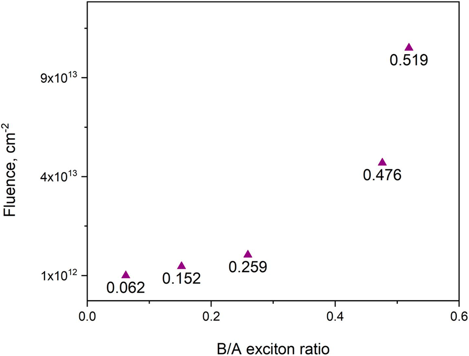
The number of introduced defects is expected to progressively increase with increasing ion fluence. At higher ion fluences (≥1 × 1015 cm−2), the accumulated damage eliminates both exciton peaks in MoS2 as can be seen in Fig. 1. To further illustrate this trend, Fig. 2(a) plots both A1s and B1s exciton peaks as a function of increasing ion fluence. As can be seen from Fig. 2(a), exciton peaks are getting closer, which generally indicates a reduction in the spin-orbit coupling in MoS2, but additional work is needed to confirm this observation. Figure 2(b) plots the B/A exciton ratios as a function of increasing fluence.
Relationship between A and B exciton peaks and ion fluence in irradiated MoS2 samples, where (a) plots A1s and B1s exciton peak energies as a function of increasing ion fluence and (b) illustrates how B/A exciton ratios change with ion fluence.

In the past, the B/A exciton ratio has been used to estimate the defect density of pristine MoS2 flakes. High-quality MoS2 monolayers grown using CVD method were shown to have B/A ratios between 0.01–0.03 [Reference McCreary, Hanbicki, Sivaram and Jonker31]. The B/A ratio of unirradiated MoS2 used in this study was 0.03, which is comparable to that of CVD grown MoS2 and indicates good initial sample quality. On irradiation to the lowest fluence of 1 × 1012 cm−2, the B/A ratio doubles (0.06) and reaches 0.52 at the intermediate fluence of 1 × 1014 cm−2. Thus, up to the fluences of 1 × 1014 cm−2, the lattice remains crystalline and defect densities in MoS2 can be controlled, whereas at higher fluences, large number of introduced defects distorts excitonic structure of the material.
Preliminary DFT calculations were conducted in parallel to our experimental work. Theory indicates that point defects, such as sulfur vacancies, are the most common defect type in MoS2. The relaxation of the structure is minimal on formation of vacancies, and neutrally charged defects retain trigonal symmetry. DFT calculations of the formation energies of the S vacancy [illustrated in Fig. 3(a)] and S divacancy [shown in Fig. 3(b)] in monolayer MoS2 in the Mo-rich/S-poor limit are shown in Fig. 3(c) as a function of the Fermi-level position. The valence and conduction band edge positions calculated with respect to the vacuum level are indicated by the vertical dotted lines. The slope of the formation energy plot corresponds to the most stable charge state for the defect over that range of Fermi energies.
DFT simulation results showing schematics of (a) S vacancy V s and (b) S divacancy V s2, where Mo atoms are shown in purple and S in yellow, and (c) formation energies of V s and V s2 in monolayer MoS2 in the Mo-rich/S-poor limit, as a function of Fermi level position. For both defects, the 0/−1 CTL is predicted to be within the band gap and to be associated with a defect level close to the conduction band minimum.

The calculated formation energy of the single S vacancy in the Mo-rich/S-poor limit is about 1.25 eV, which is in good agreement with the values reported in the literature [Reference Tongay, Suh, Ataca, Fan, Luce, Kang, Liu, Ko, Raghunathanan, Zhou, Ogletree, Li, Grossman and Wu4, Reference Komsa and Krasheninnikov24, Reference Naik and Jain39, Reference Noh, Kim and Kim40]. The S vacancy formation energy in the S-rich limit is higher, about 3 eV, but even under those conditions it is still predicted to be one of the lowest energy intrinsic point defects. The formation energy of the S divacancy in the Mo-rich/S-poor limit is calculated to be about 2.4 eV, indicating only a slight binding energy between S vacancies. Our calculations predict that both 0/−1 charge transition levels (CTLs) fall within the band gap and are about 1.55–1.65 eV above the valence band minimum (VBM) in monolayer MoS2, again in good agreement with other computational studies [Reference Tongay, Suh, Ataca, Fan, Luce, Kang, Liu, Ko, Raghunathanan, Zhou, Ogletree, Li, Grossman and Wu4, Reference Komsa and Krasheninnikov24, Reference Naik and Jain39, Reference Pandey and Soni41]. The CTLs indicate the presence of (deep acceptor) defect states in the gap which could trap excitons.
Experimentally, we observe a sharp peak at ∼1.82 eV in the PL spectra of the sample irradiated to 1 × 1016 cm−2 [see Fig. 4(a)] and ∼1.70 eV in the sample irradiated to 1 × 1015 cm−2 [see Fig. 4(b)]. These peaks were not observed in samples irradiated to lower fluences and are believed to arise from the valley excitons migrating to defects such as sulfur vacancies, which are formed in higher concentrations under higher irradiation fluences. Excitons have been known to migrate to defect bound states in monolayer MoS2, and the PL peaks (at 1.70 and 1.82 eV) have been previously verified to be reflective of a defect bound state [Reference Pandey and Soni41, Reference Saigal and Ghosh42, Reference Cao, Feng, Shi, Niu and Wang43]. With DFT predicting that V s and V s2 are the most favorable defect types that form in MoS2, it is likely that the observed PL peaks are associated with these defects. DFT predicts that the defect states introduced by S vacancies and divacancies are toward the top of the band gap, which is consistent with the energies of the observed PL peaks. However, more detailed calculations at higher level of theory are needed to obtain a better quantitative comparison between experiments and theory.
PL peaks observed in samples irradiated with 3 MeV Au ions to fluences of (a) 1 × 1016 cm−2 and (b) 1 × 1015 cm−2.

It is possible that the sample irradiated to the highest fluence has amorphized and the observed line could be reflective of the crystalline-to-amorphous transition. While the free-standing specimens irradiated to the same fluence were determined to be crystalline in nature through transmission electron microscopy imaging, specimens on the substrate cannot be examined in the same fashion. Thus, we cannot rule out the possibility of the amorphization of MoS2 flakes at the highest irradiation fluence due to extensive collision cascades in the substrate that introduce additional damage to MoS2. Further studies will be conducted to ascertain the crystalline state of the specimen and confirm that the observed peaks indeed correspond to V s and V s2.
Although initial assessment is promising, more work needs to be performed to match experimental results with theoretical predictions. Theory agrees that the A1s and B1s excitons should be within the energy range determined experimentally in this work. Nonetheless, DFT has limitations such as underestimation of the band gap and not considering exciton binding in these systems. DFT calculations can predict defect formation energies and the effect these defects can have on optical response of the material; they are difficult to match experimentally. For instance, due to the limitations of standard ground state DFT with semi-local functionals, we are unable to make quantitative predictions of the energy of such transitions for direct comparison with the experimental results. Therefore, further work needs to be performed to achieve better integration between experiments and modeling.
Beyond controlling neutral excitons, defects can bind photoexcited electron–hole pairs and transfer the exciton spectral weight to trions. We observe the photoemission splitting between bound and free trions, as can be seen from Fig. 5(a), where bound trions are illustrated in blue and the free trion in red. The inset in Fig. 5(a) depicts the position of electrons and holes with respect to E F in a trion. Figure 5(b) highlights the difference between bound and free trions in MoS2. In the sample irradiated to the fluence of 1 × 1015 cm−2, both free and bound trions are present within the same PL spectrum. The lifetimes of the states are much longer than the trion/exciton lifetimes, as PL spectra of irradiated MoS2 samples remains unchanged weeks after irradiation experiments.
(a) Dependence on ion fluence of the trion peaks and (b) corresponding schematic illustration of the bound and free trions in MoS2. The inset in (a) is a schematic representation of the location of electrons and a hole in respect to Fermi energy level in trion.

It is known that 2H–MoS2 breaks inversion symmetry in a singular layer but restores it in even number of layers [Reference Noh, Kim and Kim40, Reference Cao, Feng, Shi, Niu and Wang43]. The lack of inversion symmetry in monolayer MoS2 (that arises due to the coupling of valley and spin degrees) allows manipulation of the single valley using defects. Furthermore, bulk MoS2 is an indirect band gap material with a band gap of ∼1.2 eV, which transitions to a direct band gap semiconductor with an optical band gap of ∼1.87 eV when thinned to its monolayer form [Reference Gusakova, Wang, Shiau, Shaposhnikov, Borisenko, Gusakov and Tay44]. In this study, we did not fabricate monolayer MoS2 and presented data averages over the response of mono-, bi-, and tri-layered flakes, which highlights the versatility of our approach. In the future, the response of mono- and bi-layer flakes to irradiation will be investigated individually to determine if there is a correlation between defect-bound states and number of layers.
Because atomic structure of MoS2 is trigonal prismatic with hexagonal lattice occupied by one Mo and two S atoms, both highest valence bands and lowest conduction bands of MoS2 primarily form from Mo d-orbitals [Reference Li and Galli45, Reference Mattheiss46]. Previous theoretical calculations indicated that strongly localized Mo d-orbitals are primary contributors to the conduction band states at the K point, which have minimal interlayer coupling. However, linear combination of Mo d-orbitals with antibonding S p z-orbitals near the Γ point can lead to strong interlayer coupling. The defects introduced in the course of irradiation can reside between layers and alter d-electron physics. Thus, our work demonstrates the feasibility of engineering novel optical behaviors in these materials using defects, which were previously thought to be detrimental to device performance.
Conclusion
In this study, the value of defect engineering in tailoring optical response of low-dimensional MoS2 flakes was demonstrated. We conducted a systematic study of the scientific phenomena that define optical properties of MoS2 and attempted to establish a correlation between optical properties and defects. Although previous studies indicate that intrinsic defects and other structural imperfections are not necessarily detrimental to the properties of the material, the role of extrinsic defects in defining the properties of MoS2 was not clear. We illustrate that irradiation-induced defects provide benefits to optical properties of these two-dimensional materials and can be used to bind excitons and trions to enhance device performance and enable unprecedented functionalities. With the study of structural defects in two-dimensional materials still in its infancy, additional work should be conducted in the future to ensure that the gap between experiments and computational work is bridged and has a sound foundation.
Materials and methods
Experimental details
Molybdenum disulfide ultrafine powder with average particle size of ∼90 nm and specific surface area of ∼35 m2/g was purchased from the Graphene Supermarket (Reading, MA). Before irradiation studies, the quality of MoS2 was ascertained in FEI Tecnai F20 scanning/transmission electron microscope (S/TEM) operated at an accelerating voltage of 80 kV. Figure 6(a) provides a representative overview of an individual MoS2 flake, with an insert showing its crystallographic structure, consistent with 2H-MoS2. Figure 6(b) shows a high-resolution micrograph of the MoS2 atomic structure, which is in good agreement with the structure predicted by DFT calculations provided in Fig. 6(d).
Overview of the MoS2 samples used in this study: (a) TEM micrograph of the MoS2 flake, where the inset reflects the 2H phase of the material; (b) high-resolution TEM micrograph of the atomic structure; (c) optical micrograph of large area pristine MoS2 on Si/SiO2 substrate; and (d) top view and side view of the atomic structure of monolayer MoS2, where Mo atoms are depicted in purple and S atoms in yellow.

For irradiation studies, MoS2 powder was placed into a 20 mL vial, submerged in an anhydrous N,N-dimethylformamide (99.8% purity) from Sigma Aldrich (St. Louis, MO) at a concentration of 20 mg/mL, and sonicated for 3.5 h. After completion of the sonication, flakes were transferred to a Si(001) substrate with 300 nm thickness of SiO2. Figure 6(c) is a representative example of the flakes that were obtained using this methodology and shows an optical micrograph of large area pristine MoS2 flake on Si/SiO2 substrate. Note that the flakes obtained using dispersion/sonication techniques varied in thickness (from 0.85 to 2.33 nm) and contained mono-, bi-, and tri-layers of MoS2.
Specimens were subjected to 3 MeV Au2+ ion irradiation at room temperature using a 1.7 MV General Ionex tandem accelerator. The ion fluence ranged from 1 × 10¹² to 1 × 1016 cm−2. The target chamber pressure during the irradiation was at about 6 × 10⁻⁸ torr. PL spectroscopy was performed on a Horiba Jobin-Yvon LabRam ARAMIS microRaman with 1800 g/mm grating and a cooled CCD detector. The excitation laser used was 632.8 nm (1.96 eV) HeNe, processed at 298 K (±2 K). The laser power on the sample was about 130 μW, which has been proven to have a good signal-to-noize ratio on monolayer materials [Reference Burak Aslan, Datye, Mleczko, Sze Cheung, Krylyuk, Bruma, Kalish, Davydov, Pop and Heinz47]. To avoid the local heating effect that may be induced by the laser, we used a large density filter (50% transparency), analyzed our sample for any visible damage, and checked the intensities of the peaks in the spectra, as decreasing intensity peaks signify heating damage to the material.
Computational details
We computed defect formation energies using density functional theory (DFT) as implemented in the Vienna ab initio simulation package (VASP) [Reference Kresse and Furthmüller48]. We performed calculations using projector-augmented wave potentials [Reference Kresse and Furthmüller48, Reference Blöchl49, Reference Kresse and Joubert50] and treat the exchange-correlation using the Perdew–Burke–Ernzerhof (PBE) [Reference Perdew, Burke and Ernzerhof51] generalized gradient approximation functional. A plane wave cutoff energy of 520 eV, and Methfessel–Paxton smearing [Reference Methfessel and Paxton52] with smearing energy width of 0.10 eV and Γ-centered Monkhorst–Pack k-point meshes [Reference Monkhorst and Pack53] were employed for Brillion zone integration. Defect calculations were performed in a 4 × 4 supercell, with 20 Å vacuum spacing between layers, and a 3 × 3 k-point mesh.
The formation energy E f[X q] of a point defect X with charge q is determined by DFT calculations using a supercell approach following:
 $$E^{\rm{f}} \left[ {X^{\rm{q}} } \right] = E_{{\rm{tot}}} \left[ {X^{\rm{q}} } \right] - E_{{\rm{tot}}} \left[ {{\rm{pristine}}} \right] - \Sigma _i n_i \mu _i + qE_{\rm{F}} + E_{{\rm{corr}}} \quad ,$$
where E tot[X q] and E tot[pristine] are the total DFT-derived energies of the supercell containing the defect X and the pristine supercell respectively, n i is the number of atoms of species i added/removed, μ i is the corresponding chemical potential of the species, and E F is the Fermi energy. The final term E corr corrects for the artifacts introduced by treating charged defects in the periodic supercell approach, which was evaluated using the method developed by Freysoldt and Neugebauer [Reference Freysoldt and Neugebauer54].
Acknowledgments
The work was supported by the U.S. Department of Energy, Office of Science, Basic Energy Sciences, under Award #DE-SC0019014 “Establishing defect-property relationships for 2D-nanomaterials.” RGH and AMZT time was supported by the National Science Foundation under Awards 1748464 and 1539916.


 Open access