


Introduction
Modern expeditious evolution in wireless communication is solemnly provoking electromagnetic (EM) interference (EMI) and contaminating the environment with the EM pollution. Currently, EM radiation has turned out to be the fourth most crucial provenance of public pollution besides air, water, and noise pollution. It influences the typical behavior of systems or devices as well as is hazardous to all living beings. Hence, there is a growing demand for the development of suitable materials and techniques to suppress the consequences of the EM radiation. The use of EM metamaterial (MM) is a promising solution to the problem of EMI [Reference Munk1]. The EM MMs are generally described as artificially engineered homogeneous medium implemented by the use of sub-wavelength metallic or dielectric elements that unveil the unusual EM characteristics which do not prevail in the natural world [Reference Veselago2]. These characteristics are conceived due to their structure rather than the constitution of the material. The unusual characteristics of the MMs depend on the shape, size, and geometry of the structure instead of their constitution [Reference Vu, Le, Dinh, Trinh, Yue, Le and Vu3]. Numerous exotic characteristics of MM have already been revealed, studied, and implemented in various sectors [Reference Capolino4–Reference Tong15]. The MMs can individually modify effective permittivity (ε) and permeability (μ) by suitably adjusting its structural parameters. The MMs have captivated the attention of numerous researchers because of the unusual properties exhibited by them such as double negative behavior, left-handed behavior, negative refractive index, backward wave propagation, negative phase velocity, etc. [Reference Caloz and Itoh14]. The applications of MMs are of interdisciplinary nature covering electromagnetics, optics, nanoelectronics and biomedical devices as well as expanding from low microwave to visible wavelengths [Reference Holloway, Kuester, Gordon, O'Hara, Booth and Smith16–Reference Shelby, Smith and Schultz18]. One of the promising applications of the MM is in the field of designing EM absorbers (EAs), where the required properties of the MMs can be smartly accomplished by suitably adopting a particular design and structure. The perfect MM absorber (MA) is one of the highly developed sectors among various accomplishments of the MMs.
The EAs can efficiently dissipate the EM energy into heat, resulting in significant reduction of the reflected waves along the direction of echo. The structure of the MA is basically composed of unit cells arranged in a periodic manner. The structure consists of a top conducting layer and a bottom ground plane isolated by a dielectric interlayer. The dielectric interlayer is responsible for the regulation of the input impedance  $[Z(\omega )=\sqrt {\mu (\omega ) / \epsilon (\omega )}]$ of the MA. It also makes sure that the MA perfectly matches the impedance of the free space $(Z_0=\sqrt {\mu _0 / \epsilon _0} \approx 120\pi \approx 377\Omega )$. Consequently, the incident waves can be guided into the dielectric interlayer, which consumes the penetrating waves as much as possible. The structure yields equivalent inductances (L) and capacitances (C) as a result of the conducting patterns and the gaps respectively among the patterns, which leads to the LC equivalent circuit. The underlying bottom ground plane with thickness more than skin depth prevents the incident waves from passing through the structure. This arrangement reduces return losses and ultimately causes almost perfect absorption at resonant frequencies [Reference Munaga, Ghosh, Bhattacharyya and Srivastava19].
In the MAs, the surface charges are activated with an electric field which results in magnetic response and causes resonant absorption. The currents are generated due to the coupling of harmonizing field of the incident EM wave with the electric and magnetic field responses. As a result, the structure of the MA consists of circulating and anti-parallel currents. The magnetic responses are caused by the circulating currents whereas the electric responses are the result of anti-parallel currents. This strong coupling yields the electric and magnetic resonances to excite at the same resonance at the same time and results in a highly localized EM field enhancement at the working resonance. This field enhancement yields almost complete absorption of the EM waves at the resonance provided that the impedance matching condition [Z(ω) = Z 0(ω)] is satisfied. Therefore, entire incident energy is confined in the MA that means reflection is minimized on the contrary of absorption. Thus, approximately null reflection and almost perfect absorption are achieved due to the confinement of EM energy in the MA [Reference Montaser20].
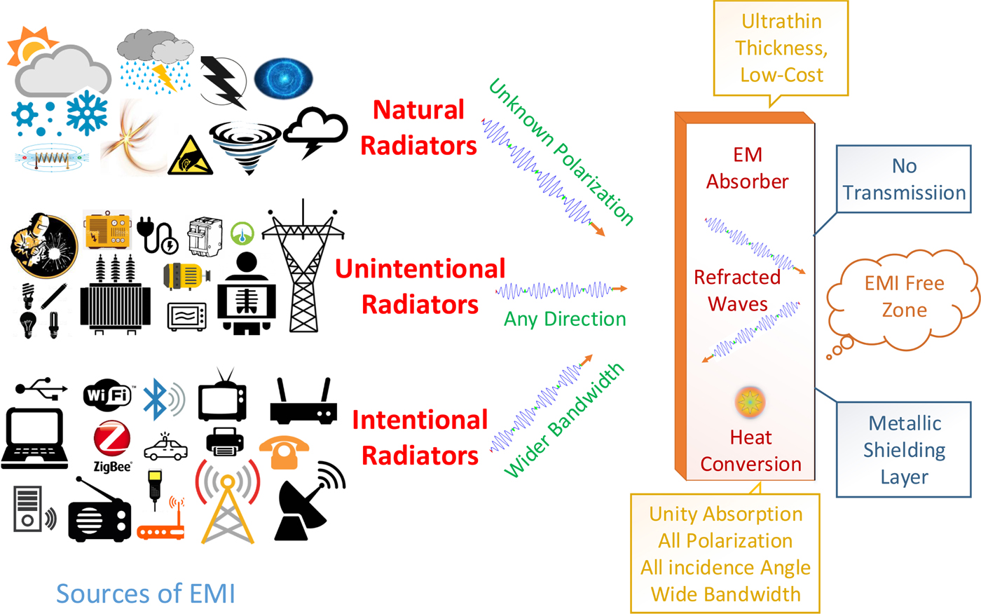
The manifestation of perfect MA primarily achieved by Landy et al. [Reference Landy, Sajuyigbe, Mock, Smith and Padilla21] in the microwave domain started a revolution in the field of the MAs. Thus, resulting in tremendous work for the exploration of MM-based absorbers from the microwave to the optical bands. Due to the straightforward implementation of the MAs in the microwave and the terahertz spectrum by suitably specifying a particular design and structure, these two frequency bands recently acquire most of the attention for implementing the MAs. In most of the practical applications, the nature of EMI is unknown, in the sense that it may occur over a broad range of frequencies, may be of any polarization and may originate from any direction. Hence, ultrathin absorbers which are insensitive to all polarization angles, can absorb EMI over a wide range of frequencies and for all angle of incidences, as well as possess near perfect absorption is the need of perfect EAs as illustrated in Fig. 1. Unfortunately, achievement of all these objectives simultaneously in a MA is very tough. The absorbers reported so far in the literature mostly succeeded in achieving only one or two aims while sacrificing the others. There is just a limited progress towards the achievement of perfect EAs besides many efforts made by numerous researchers to develop an efficient technique to acquire all these objectives simultaneously. The EAs with such characteristics are highly desirable for stealth technology since EAs can efficiently reduce the reflection and the transmission of the EM waves to smallest possible level. This property of the EAs has made them the most suitable candidate for the suppression of EMI.
Illustration of EM absorber in the current scenario.
As described earlier, achieving perfect absorption over a wide range of frequencies is very tough. It is nearly unfeasible to acquire more than four absorption peaks using only one resonator [Reference Yoo, Kim, Hwang, Rhee, Kim, Kim, Cheong, Chen and Lee22]. Although the bandwidth at the resonant frequency is narrow, it is possible to have five or six distinct peaks by the single patterned resonator [Reference Wang and Wang23]. Even if multiple absorption bands are realized, it is difficult to reduce the interval between resonant frequencies and to maintain the absorption at the same time unless multilayered absorbers are employed [Reference Wang, Wang, Wang, Huang, Li and Zhai24]. The appropriate structural design of resonator's microstructure is a simplified approach to control the useful EM parameters to manipulate the desired EM response. Recent advances in micro-nano technology are helpful in achieving many flexible designs of resonator's microstructure. The composite structures have also been designed to acquire broadband resonance which ordinary mediums do not possess [Reference La Spada and Vegni25]. Other techniques include alternate placement of transparent spacers and ultrathin resistive layers like graphene, indium tin oxide (ITO) or other conducting oxides with excellent solar transmission performance [Reference Jang, Youn, Shin and Guo26–Reference Batrakov, Kuzhir, Maksimenko, Paddubskaya, Voronovich, Lambin, Kaplas and Svirko28], which provides improved results.
One of the oldest invention in radar absorbent material is the Salisbury screen [Reference Fante and Mccormack29]. It consists of a thin glossy screen isolated by a conducting ground plane with a lossless dielectric material of a quarter-wavelength thickness. Unfortunately, it suffers from narrow absorption bandwidth and is also bulky. In order to increase the absorption bandwidth, the Jaumann absorber [Reference Du Toit30] is proposed by extending resistive sheets and dielectric materials. Apparently, the overall thickness of the absorber becomes wider than that required, in many practical problems. A simple combination of a quarter wavelength thick lossy homogeneous layer placed on a conducting plane is considered as a Dallenbach layer. The lossy layer offers a specific amount of electric and magnetic losses which helps in matching the impedance of the layer to that of the free space. Hence, there is no reflection from the surface of the layer and the losses presented by the layer absorbs the incident EM waves at its resonance. However, broadband absorption is possible only when a sufficient number of layers are stacked together.
Another technique to increase the absorption bandwidth is the use of frequency selective surface (FSS) [Reference Munk31] with highly absorbent materials [Reference Park, Choi and Kim32–Reference Baek, Choi, Lee, Cho, Petrov, Agnesi, Pasiskevicius, Yeom, Kim and Rotermund34]. The structure of FSS comprises of suitably arranged conductive patterns placed on a dielectric medium. The FSS-based absorbers possess good absorption properties. However, these absorbers are bulky, breakable, and have high surface mass density. Moreover, these absorbers are subjected to dynamic thickness-bandwidth compromise, ultimately controlling their application areas. Circuit analog absorbers (CAAs) [Reference Ghosh, Bhattacharyya and Srivastava35] can provide absorption over a wide range of frequencies both for normal and obliquely incident radiations. The structure of CAA consists of one or more sheets composed of both resistive and reactive components arranged in a periodic manner at a quarter wavelength above the ground plane. Such an arrangement may be considered as a lossy FSS. A large number of techniques are investigated to enhance the absorption bandwidth of the CAAs by exploiting hybrid materials such as resistive-capacitive materials, resistive-inductive materials, and patterns like dipoles, crosses, triangles etc. However, these designs are quite complex and have a slow and tedious manufacturing process.
The impedance matching between the incident and absorbing media can very well be achieved by using the graded dielectric absorbers such as pyramidal, tapered, and matching absorbers [Reference Tong15]. For matching the impedance between the free space and the absorber, the pyramidal absorbers use canonical or pyramidal structures for the progressive transition of the impedance. In other two types of impedance matching options, the tapered loading absorber makes use of a slab made up of low loss and lossy material composition and the matching layer absorber uses a thin transition layer for impedance matching in order to minimize the thickness of the gradual transition materials. The pyramidal absorber outperforms all the other two types of absorbers in terms of providing higher attenuation over the wide frequency range and wide angle of incidence. However, the wedge-shaped pyramidal structures are thick, bulky, and made up of fragile material.
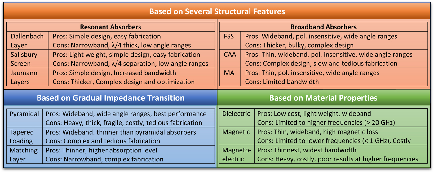
The dielectric, magnetic or magneto-dielectric materials may be employed for absorber coatings where one, two or several layers of these materials or grading of these materials are mostly used. The absorbers constituted using dielectric materials are generally thicker than the absorbers using magnetic materials. It is because of the fact that the dielectric absorbers have no magnetic properties, the loss mechanism is purely dielectric, and their permittivity possess smaller real and imaginary part in comparison with the magnetic absorbers possessing higher real parts of both permittivity and permeability. The hybrid magneto-dielectric absorbers are highly efficient, thinnest, and provide the widest bandwidth since they combine the advantages of both dielectric and magnetic materials offering large dielectric and magnetic losses. For high-frequency application, over the range of 100 MHz–20 GHz, dielectric absorbers are preferred, for the lower range of 30 MHz–10 GHz, the magnetic absorbers are preferred and for broadband EMC testing in the range of 30 MHz–20 GHz, the magneto-dielectric absorbers are chosen [Reference Tong15]. EAs may be categorized based on several structural features, gradual impedance transition, and material properties. A comparison of some of these realized structures with their pros and cons are summarized in Fig. 2.
Advantages and disadvantages of some EAs based on several structural features, gradual impedance transition, and material properties.
Composite materials are useful for achieving desired absorption bandwidth but is not sufficient for attaining minimum possible coating thickness. Hence, utilization of an efficient technique along with suitable absorbent materials is highly desirable for exploring the innovative field of EAs. It is clear that such multiobjective design problems are highly complex. Therefore, use of optimization techniques such as Genetic Algorithm (GA) [Reference Sun, Gu, Chen, Li, Liu, Xu and Zhou36–Reference Wang, Kong, Cheng, Bao, Yu, Miao and Jiang38] becomes an essential component in such issues to ensure that the final design attains the desired characteristics. Therefore, in this review, an effort has been made to justify the need for a low-cost thin microwave absorber for achieving wide absorption bandwidth and superior absorption properties along with polarization-insensitivity, wide incident angle, and near perfect absorption.
The meaning of various acronyms used in this paper is listed in Table 1. The parameters given to describe the performances of different absorbers in this paper correspond to the simulation results.
Acronyms used in this paper

Historical Background
The utilization of MMs as the EAs is firstly carried out by Landy et al. in 2008 for near perfect absorption [Reference Landy, Sajuyigbe, Mock, Smith and Padilla21]. The experiment shows nearly 100% absorption of the EM waves penetrating through the designed MA. The structure is compact with adequately low thickness than that of the conventional EAs. The dielectric loss and ohmic loss are found to be the possible cause of the absorption mechanism in addition to the LC resonance of Split Ring Resonators (SRRs). The work of Landy started a revolution in this field to explore the perfect MA. The insensitiveness of polarization in the MA for a wide angle of incidence is investigated by Wang et al. in 2009 [Reference Wang, Koschny and Soukoulis39]. Li et al. used triple layered unit cells for a resonant dual band MA in 2010 [Reference Li, Yang, Hou, Tian and Hou40]. In 2011, Cheng et al. utilized the concept of SRRs to achieve perfect absorption [Reference Cheng, Yang, Cheng and Wu41] and Lee et al. enhanced the absorption bandwidth of the MA by placing two absorption peaks close to each other. In 2013, Bhattacharyya et al. obtained a triple band absorption by combining similar structures of different sizes [Reference Bhattacharyya, Ghosh and Vaibhav Srivastava42]. Similarly, concentric squares and circular rings are arranged by Bian et al. [Reference Bian, Liu, Wang, Kong, Zhang, Ma and Yang43] and Ayop et al. [Reference Ayop, Abd Rahim, Murad, Samsuri and Dewan44] in a particular manner to explore a triple band MA to enhance the bandwidth and achieve the polarization independence. Gong et al. realized a MA based on sectional asymmetric structures to manipulate the absorption bandwidth and maintain other essential properties as per the requirement [Reference Gong, Zhan, Yang, Wang, Liu, Zhao and Liu45]. These MAs suffer from narrow absorption bandwidth caused by the resonant behavior of the MM, thereby, restricting their essential application areas.
One of the first significant theories to investigate the behavior of the MMs is effective medium theory [Reference Zhang and Wu46]. It replaces the scattering objects distributed on a thin medium by averaging the local electric and magnetic fields when its wavelength is kept considerably higher than the lattice constant of its unit cell. The impedance matching principle provides only a qualitative investigation of the behavior of the MA. Transmission line model is a useful approach for normally incident EM waves. However, it ignores the interaction between different layers of the MA. Interference theory, thus, emerges as an approach which does not suffer from such problems. It can investigate both qualitatively as well as quantitatively, the characteristics of the MA. It can analyze the interactions among different internal layers of the MA. It also has the advantage to tackle complex structures and study the behavior of the MA for oblique angle of incidences. Initially, interference theory is used for the investigation of single and multiple band MA [Reference Shen, Yang, Zang, Gu, Han, Zhang and Jun Cui47]. Interference theory of perfect MA neglects any near-field interaction and explains it as a superposition of multiple reflections [Reference Chen48]. Thus, at the resonant frequency, the incident field destructively interferes with the reflected waves from the surface as they cancel out each other and eventually lead to the absorption of the EM waves. The implementation of the MAs for wideband applications is also possible with the interference theory. Therefore, Chen et al. implemented a MA to explore its wideband characteristics at both normal and oblique incidences by using the interference theory [Reference Chen, Hu, Wang, Huang, Wang, Hu and Liu49]. However, these structures pose difficulties regarding fabrication and measurement.
In order to widen the absorption bandwidth, a number of approaches have been proposed. Multilayering is one of the most straightforward methods for bandwidth enhancement, and utilization of GA can make the task even simpler than before [Reference Soheilifar and Sadeghzadeh50]. Lee and Lee incorporated multiple structures of distinct proportions into a single unit cell to widen the working bandwidth [Reference Lee and Lee51]. Kollatou et al. developed highly absorbing wideband MA by utilizing scalability property of MMs [Reference Kollatou, Dimitriadis, Assimonis, Kantartzis and Antonopoulos52]. Various arrangements of donut-based resonators are employed by Park et al. to achieve a multiband MA [Reference Park, Van Tuong, Rhee, Kim, Jang, Choi, Chen and Lee53]. Gu et al. combined the absorption peaks of different hexagonal metal dendritic units that are placed close to each other in order to broaden the bandwidth of an isotropic MA [Reference Gu, Su and Zhao54]. Incorporation of lumped elements in the structure of the MA is an efficient method to achieve a broad bandwidth for microwave applications [Reference Zuo, Yang, He, Mao and Liu55]. Unfortunately, the practical realization of such a technique is very tough at terahertz, infrared, and optical frequencies. However, there is still a further scope of improvement in the absorbing properties in terms of the parameters of the MAs. Realization of the MAs which are simple to design, easy to fabricate and possess high absorptivity, smallest possible thickness, and broadband characteristics are still in progress.
Issues of Bandwidth and Thickness
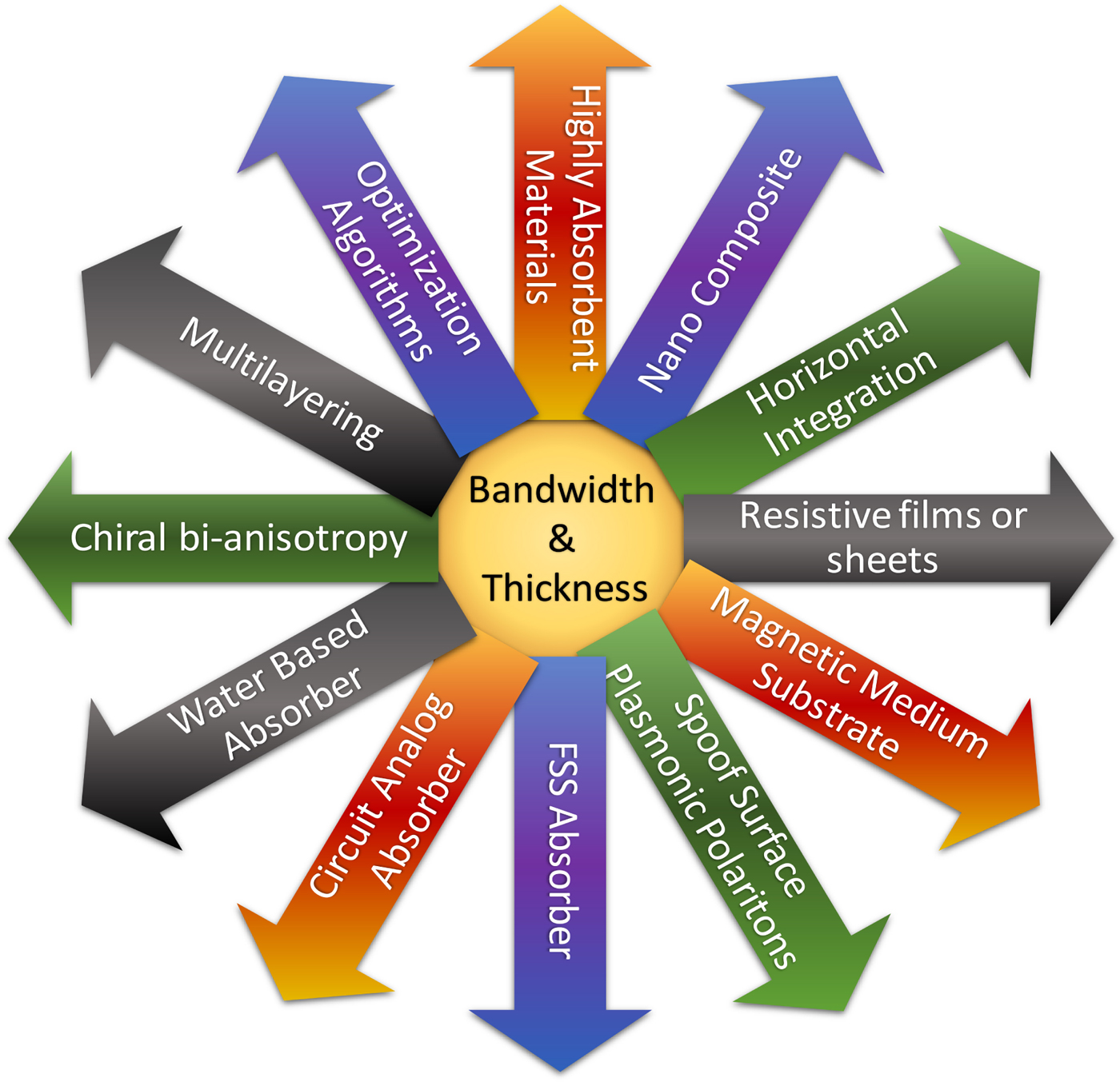
The exotic properties of the MMs give rise to the absorption rate of the MAs. However, the electric and magnetic resonant behavior of the MM limits the absorption bandwidth of the MA, ultimately limiting their essential applications in most of the fields that require a wide working band. The implementation of a thin MA for almost perfect absorption in a small range of frequencies is not hard to achieve. However, the problem becomes challenging when perfect absorption is needed over a wide range of frequencies with minimal thickness. One of the essential parameters that greatly influence the absorption rate and the working frequency of the MA is its thickness. Thin EAs can absorb the incident EM waves completely, but only over a small range of frequencies. The absorption bandwidth and thickness are two conflicting requirements. There should be certain means to overcome this dynamic thickness-bandwidth constraint. Fundamentally, there is a restriction in realizing thin absorber with wideband characteristics. However, absorption through commercially available EAs need relatively large domain [Reference Vinoy and Jha56]. These absorbers are heavy and thick due to their pyramidal or wedge type outline. Therefore, light-weight and ultrathin EAs are always desirable for practical applications. A lot of researchers have tried to solve this bandwidth-thickness problem. Combining different resonant units together horizontally [Reference Vu, Le, Dinh, Trinh, Yue, Le and Vu3] or vertically [Reference Batrakov, Kuzhir, Maksimenko, Paddubskaya, Voronovich, Lambin, Kaplas and Svirko28], using highly absorbent materials [Reference Baek, Choi, Lee, Cho, Petrov, Agnesi, Pasiskevicius, Yeom, Kim and Rotermund34], incorporating lumped circuit elements in the structure [Reference Zuo, Yang, He, Mao and Liu55], utilizing high loss materials [Reference Rephaeli and Fan57], including resistive films [Reference Shen, Pei, Pang, Wang, Zhang and Qu58], using magnetic medium substrate [Reference Hokmabadi, Wilbert, Kung and Kim59] etc. are some of the approaches proposed to tackle such problem. Every approach possesses certain benefit as well as some limitation. Fig. 3 illustrates some popular techniques to overcome the issues of bandwidth and thickness of EAs.
Techniques to overcome the issues of bandwidth and thickness of EAs.
One of the most efficient methods to acquire enhanced working bandwidth is to combine various resonant units, specifying different frequencies, inside a single unit in a multilayered fashion [Reference Tang, Xiao, Xu and Liu60,Reference Long, Yin, Wang, Li, Zhu and Guan61]. The occurrence of several phenomena between multiple layers of the structure gives rise to the absorption rate of the absorber. It is evident that the multilayering approach increases the number of losses in the structure. This intensifies the absorbing properties of the structure with reduced thickness while maintaining a wide working band. Such a technique requires careful selection of the unit cell parameters. The fabrication process also becomes tough due to the presence of multiple structures in a limited space. The placement of various resonant units is also very critical to maintain near unity absorption in a broad frequency range. Such placement results in complex interaction between individual units. Many conflicting parameters also arise that change the overall performance of the structure. However, multilayering provides a good compromise between bandwidth and absorption rate of the EA by merging the resonance of every layer. It offers improved results for a perfect absorption over a broad bandwidth. Multilayering using different material integration have also been used to enhance the working bandwidth and reduce the thickness with better absorbing capability. However, the prediction of the sequence of various materials, as well as the thickness of layers, is a complicated process. Therefore, optimization of these contradicting parameters of the absorber has been used to acquire the best trade-off between all these parameters to get the desired results. Several optimization algorithms have been attempted to fulfill this need such as GA [Reference Najim, Smitha, Agarwala and Singh62], artificial neural network (ANN) [Reference Najim, Puthucheri, Agarwala and Singh63], particle swarm optimization (PSO) [Reference Wang, Zhao, Cheng, Dong and Cui64] etc.
The EAs can operate over a vast range of frequencies if there is no restriction of absorber thickness. The thickness is a primary constraint in realizing a perfect EA, as evident in Jaumann absorber [Reference Du Toit30], which has limited practical applications due to the thickness. With an aim to maximize the absorption frequency as well as minimize the absorber thickness, Panwar et al. proposed a technique recently [Reference Panwar, Puthucheri, Agarwala and Singh37] to realize two layer absorber of thickness limited to 1.5 mm while maintaining the absorption rate more than 90%. GA is used for achieving the optimum solution to the problem. The double-layered absorber is implemented with Sierpinski gasket fractal FSS and heterogeneous composites of Fe3O4 − Ti particles. The dimension and shape of these particles are suitably optimized for maximum bandwidth and minimum thickness of the absorber.
The EAs have found many applications in the radio frequency (RF) spectrum, especially in the S, C, X and Ku bands. The materials made with ferrites and magnetic metals possess the absorption capability over a wide bandwidth in the RF regime. These materials can absorb EM waves with an absorption rate of more than 85% in X and Ku bands [Reference Han, Li, Wang, Liu, Li, Geng and Zhang65,Reference Qing, Zhou, Luo and Zhu66]. Snoek's limit [Reference Acher and Dubourg67] and magnetic resonant behavior of the composites cause difficulty in increasing the absorption rate in S and C bands. Li et al. integrated non-planar MMs with magnetic absorbing materials to achieve almost perfect absorption from 2 to 18 GHz [Reference Li, Wu, Wang, Guan and Zhai68]. This hybrid MA consists of two layers while maintaining lightweight characteristics. However, the hybrid absorber usually suffers from a relatively complex structure. Yin et al. implemented an ultra-broadband MA with reduced complexity and thickness [Reference Yin, Long, Li, Zhu, Chen, Guan and Li69]. The MA is designed by combining the absorption peaks of two tapered hyperbolic MM waveguide arrays as shown in Fig. 4. Both waveguides have different dimensions and broad but different bandwidths. The final structure can absorb more than 90% of the EM waves over an ultra-wide range of frequencies from 2.3 to 40 GHz. Although, the absorption peak above 0.9 absorption rate is comparatively narrow due to the presence of larger harmonic frequency next to the fundamental one. This method is very advantageous to get rid of the low absorption bands that occur in between the high absorption bands, ultimately providing greatly expanded continuous working bandwidth.
Experimental realization of two layer hybrid ultra-broadband absorber for absorption from S to Ka band. This figure is reproduced with permission from [Reference Yin, Long, Li, Zhu, Chen, Guan and Li69]. © 2015, Nature Publishing Group.

In order to achieve customized absorption in a wide range of frequencies, Pang et al. engineered the spatial k-dispersion relation of spoof surface plasmonic polaritons (SSPPs) [Reference Pang, Wang, Ma, Feng, Li, Xu, Xia and Qu70]. Plasmonic arrays can efficiently convert the incident EM waves into the SSPPs. Suitably engineered spatial dispersion relation of k-vector can provide necessary control over their absorption capability. The field confinement effect exhibited by the SSPPs can give the absorption capability to the structure by incorporating proper losses. This effect can also provide extraordinary possibilities near the asymptotic frequency. Due to the discrepancy of k-vector between space wave and the SSPPs, complete absorption cannot be achieved by this method.
FSS absorbers (FAs) are capable of producing EAs with extended working bandwidth. These absorbers are nothing but a periodic arrangement of resonators and dielectrics [Reference Munk31]. Various periodic adjustments have been made to enhance the working bandwidth of the FAs such as fractal structures, multi-ring placement, and other diverse patterns. Such absorbers possess multi-resonant property, which is beneficial for attaining proper absorption. The resonant state of the FAs can be manipulated to achieve wideband characteristics. Tunable FAs can change the resonant state easily as per requirement. The tunable FAs are designed in such a way that complete attention is given to the entire adjustable bandwidth. It does not consider the wide bandwidth resulting from a single resistor. The tuning of the resonant states of the FAs result in similar wideband characteristics of various states individually. The unit cell of the FAs may comprise multi-resonant structures as well as some active devices. The parameters of active devices in association with different periodic arrangements make the implementation of tunable FAs quite easier to accomplish wideband characteristics [Reference Kong, Yu, Liu, Zhou, He, Miao and Jiang71].
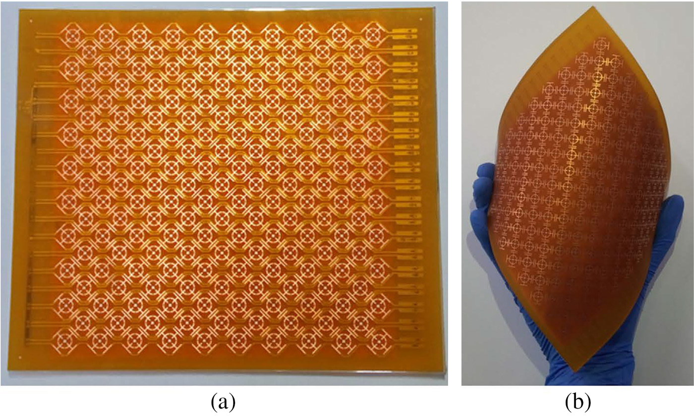
Among the most efficient methods for the accomplishment of increased absorption bandwidth, use of the CAAs is worth mentioning. Suitable selection of chip resistors and their placement in the most appropriate place in the structure of the absorber can be utilized to achieve a wideband EA [Reference Munaga, Ghosh, Bhattacharyya and Srivastava19]. Ghosh et al. investigated a multilayered CAA with the aid of resistive FSS to realize a wideband absorber [Reference Ghosh, Bhattacharyya and Srivastava35]. The upper layer of the CAA comprises an array of square loops, and some lumped resistors are incorporated into the loop. The bottom layer is made with a high impedance surface (HIS). Both layers are separated by an air spacer. The separation does not increase the overall thickness of the absorber considerably. The incorporation of bottom HIS increases the total bandwidth of the CAA by producing new resonance. The absorber has the advantage of being polarization insensitive. However, the absorber shows wideband absorption characteristics only under normal incidence of the EM waves. The performance of the absorber decreases according to the increase in the angle of incidence. The drawback of such absorbers is that these are very difficult to fabricate. Zhai et al. recently investigated a reconfigurable MA for a wideband application [Reference Zhai, Zhang, Zhang and Zhan72]. The structure consists of stubs, lumped resistors, and inductors. The working band of the absorber can reach the relative bandwidth of 55% with 90% absorptivity by suitably adjusting the lumped parameters. The parameter analysis of the loaded stubs illustrates their essential influence on enlarging the absorbing bandwidth. Also, the designed absorber has good performances on polarization-insensitiveness up to 45° of incident angle for both transverse-electric (TE) as well as transverse-magnetic (TM) polarizations. Kim et al. implemented a switchable MA by combining lumped elements and microfluidic channels in association with liquid metal alloy [Reference Kim, Lee and Lim73]. The appropriate combination of these components results in the wide absorption of a thin MA with an added benefit of flexibility and switchability as shown in Fig. 5. The MA provides successful switchable absorption performance among X and C bands by introducing a liquid metal alloy into the microfluidic channels. The MA comprises a modified Jerusalem cross resonator (JCR) and chip resistors to achieve wideband absorption. The JCR is adjusted by loading slotted circular rings into the structure. The structure is flexible due to its fabrication on a flexible substrate.
Experimental realization of switchable MA with EGaIn-filled microfluidic channels for flexibility and wideband absorption in X and C bands. This figure is reproduced with permission from [Reference Kim, Lee and Lim73]. © 2016, Nature Publishing Group.
Kim et al. proposed an ultra-wideband MA using resistive sheets working over wide angles of incidence [Reference Kim, Yoo, Hwang and Lee74]. The absorber uses periodically arranged meta-atoms. The structure comprises snake-shaped metallic patterns and metal planes separated by three resistive sheet layers between four dielectric layers. The resistive sheet plays a significant role in increasing the absorption rate. It also merges adjacent resonance peaks of the absorber because of low conductivity. Therefore, ultra-broadband absorption is accomplished by merely adding the resistive sheet layers in the MA. The broadband absorption in association with wide incident angles is achieved by employing proper parameters for meta-atoms and sheet resistance according to the thickness. The MA is independent of polarization angles because of the four-fold symmetrical rotational arrangement in the structure.
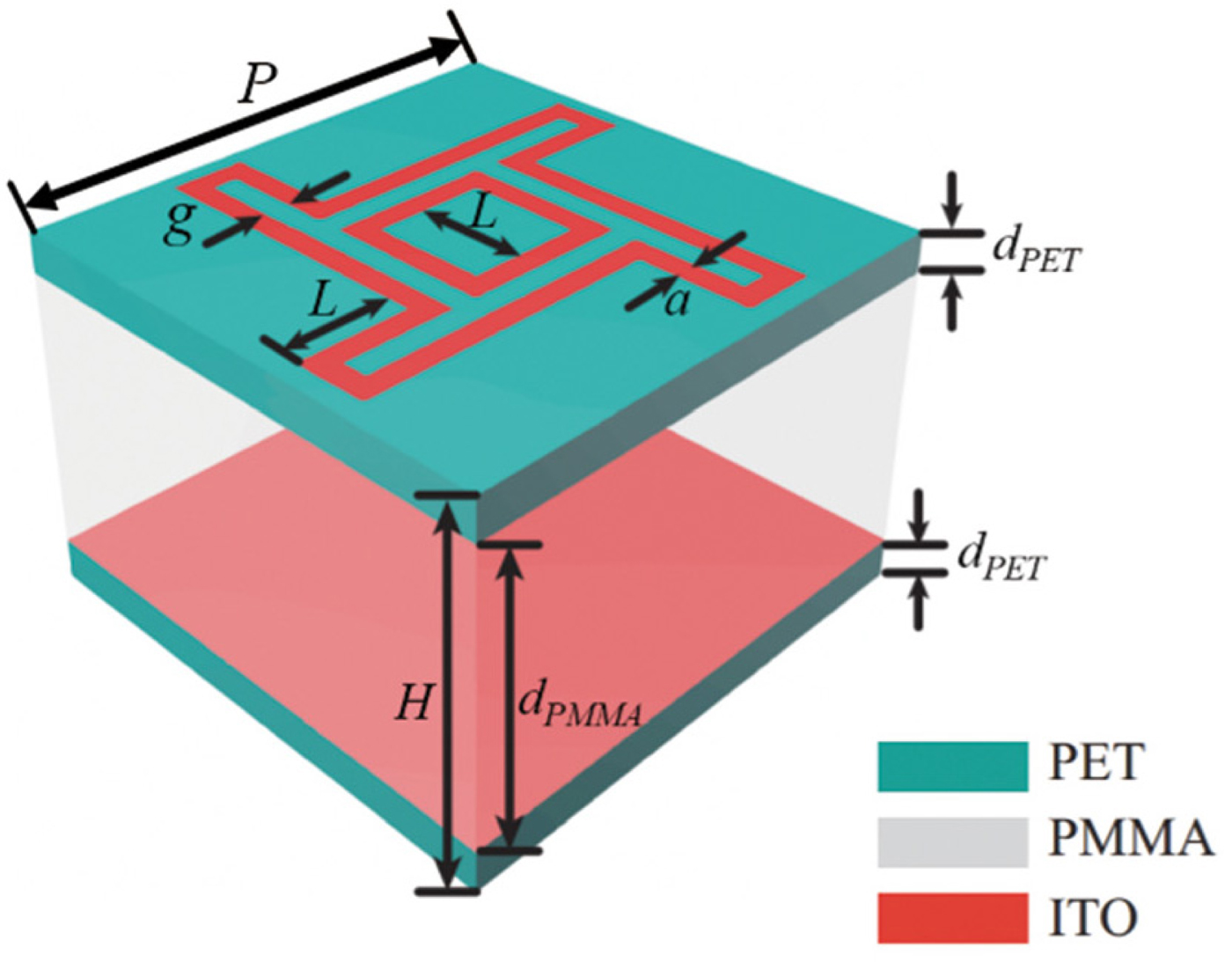
Zhang et al. presented a strategy to design a MA for simultaneous optical transparency and microwave absorption over a wide frequency band, which can be used as an optically transparent radar-wave absorber [Reference Zhang, Cheng, Yang, Zhao and Cui75]. The absorber uses a windmill-shaped structure. This is a well-defined multilayered structure composed of ITO patterns and transparent substrates including polymethylmethacrylate (PMMA) and polyethylene terephthalate (PET) as shown in Fig. 6. The windmill-shaped element is widely used as the unit cell of the microwave reflect-array antenna with the advantages of significant phase variation, broad bandwidth, and proper phase linearity. For absorber applications, the primary benefit compared with other types of the element is its multi-resonant characteristics, making it possible to improve the operational bandwidth of the absorber by adequately tailoring the resonances. The structure is highly symmetrical. Thus, the absorption performance is insensitive to the polarization direction of the incident EM waves. Since the pattern is in close proximity to the ground plane, near-field coupling gets induced, hence anti-parallel currents are generated in the top layer and the ground plane. By adjusting multi-resonant feature of the unit cell, the bandwidth of the MA is significantly improved. They achieved an optimized MA with absorptivity greater than 90% from 8.3 to 17.4 GHz. In the meantime, an excellent optical transmittance is achieved by using ITO films with moderate surface resistance. Therefore, the optical characteristics of the MM are hardly influenced by the periodic meta-atoms.
Geometrical representation of the unit cell of the multi-layered broadband optically transparent absorber for wideband absorption from X to Ku band. This figure is reproduced with permission from [Reference Zhang, Cheng, Yang, Zhao and Cui75]. ©2017, AIP Publishing.
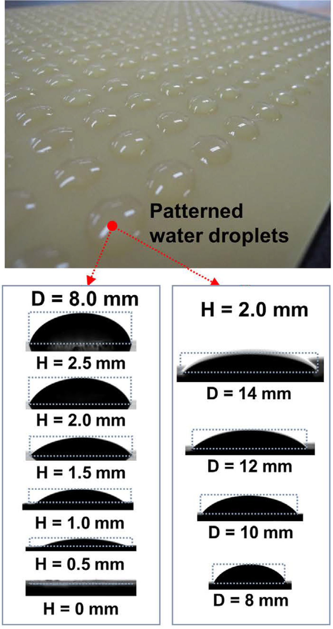
Perfect absorption of the EM waves is also possible using abundant water available in the world. The permittivity of naturally occurring water is strongly frequency dispersive at microwave frequencies. Thus, water is a promising constituent material for designing broadband absorbers [Reference Ellison76] and has gained considerable attention recently [Reference Andryieuski, Kuznetsova, Zhukovsky, Kivshar and Lavrinenko77,Reference Odit, Kapitanova, Andryieuski, Belov and Lavrinenko78]. Yoo et al. developed a perfect MA with the technique of absorption using water droplets [Reference Yoo, Ju, Park, Kim, Bong, Lim, Kim, Rhee and Lee79]. The structure follows a specific periodic arrangement of water droplets which serves as a resonator. Every droplet is placed on the top layer of the structure with a particular diameter as well as height by using the wettability of the layer as shown in Fig. 7. These two parameters of water droplet are essential for controlling the absorption rate and working bandwidth. Efficient absorption of the EM waves is achieved over a wide frequency band from 8 to 18 GHz by the meta properties of the droplets with an overall thickness of 4 mm. It is necessary to note that these water droplets are low conductive materials, whereas most metallic MMs are highly conductive materials. Pang et al. developed water as a dielectric substrate instead of a resonator to construct the MA [Reference Pang, Wang, Cheng, Xia, Zhou, Xu, Cui and Qu80]. The designed MA has a well-known metal-substrate-metal configuration, but the substrate is a combination of water and a low-permittivity material. This configuration allows tight packaging of water and simple fabrication of the absorber. By designing the hybrid substrate of thickness 3.5 mm and the parameters of the MM inclusions, broadband absorption from 6.2 to 19 GHz is achieved at the temperatures of interest with more than 90% absorptivity.
Experimental realization of water droplet-based MA with investigated diameter and height of water droplet for wideband absorption from X to Ku band. This figure is reproduced with permission from [Reference Yoo, Ju, Park, Kim, Bong, Lim, Kim, Rhee and Lee79]. ©2015, Nature Publishing Group.
Asadchy et al. explored the concept of chiral bi-anisotropy with helical elements for realizing thin and broadband EAs [Reference Asadchy, Faniayeu, Ra'Di, Khakhomov, Semchenko and Tretyakov81]. The idea of the simultaneous generation of electric and magnetic responses through a single resonant mode of the unit cell is utilized to achieve wideband absorption in a thin absorbing layer. The helical elements can provide similar dipole moments by coupling them with electric and magnetic fields. Thus, providing wide resonance without any diversion between resonant frequencies. These responses are accomplished by the current loops induced in the helix used in the unit cell array of the metasurface. This technique is beneficial for reducing the absorber thickness by increasing the number of loops of the helical elements incorporated in the metasurface.
Based on the placement of resonators and their structures, the techniques for realization of a perfect wideband MA may be categorized into the following four groups: (I) Combining several resonators of different structures together. (II) Integrating several resonators of similar structure with distinct dimensions. (III) Assembling resonators of similar structure with a certain rotational arrangement. (IV) Organizing various resonators vertically on different layers.
However, the working bandwidth is determined by the quantity of resonator. Increased working bands require a large number of resonators, which is a restriction in terms of fabrication of the perfect MA due to the bulkiness of the structure.
Issues of Polarization and Incidence Angle
The practical requirement of an effective EA is its insensitivity to the orientations of incident EM radiation as well as polarization in addition to the wide working band, higher absorption, and lower thickness. Despite the high absorption rate along with the complications of bandwidth and thickness, many EAs suffer from the problems of polarization sensitiveness and narrow angles of incidence. Various techniques have been adopted to resolve these issues of the EAs to accomplish perfectness in the absorbers. However, the majority of all these techniques are beneficial at terahertz and optical bands and does not show significant benefit at microwave frequencies. The published works have reported that the geometry of the absorber becomes complex, bulky, and unmanageable with the rise in the working bandwidth and incidence angles. An increase in the incidence angle of the EM waves causes weak coupling among the layers of the absorber. Especially, magnetic coupling becomes weak due to the reduction in the magnetic field component with the rise in the angle of incidence. Consequently, it causes inefficient excitation of magnetic resonance. It results in a decrease in the absorption rate and also affects other essential parameters of the EA. As far as the MAs are concerned, the traditional ones are highly sensitive to the angle of incidence and polarization of the incident EM waves. The waves may incident from any direction, at any angle, and with any polarization. In fact, the absorbers under practical consideration do not know any property of incident waves. Therefore, there is need of highly intelligent absorbers that can achieve perfect absorption in any practical scenario by considering every constraint to balance every requirement.
For example, Shi et al. recently designed an ultra-broadband, wide-angle polarization-insensitive MA at microwave frequencies [Reference Shi, Li, Hao, Li and Liang82]. This absorber produces a proper absorption above 80% at a normal incidence between 6 and 16.2 GHz, but at an oblique incidence with the incident angle smaller than 45° absorption above 60% is achieved. Munaga et al. implemented a polarization insensitive absorber (PIA) using lumped elements on a fractal structure applicable for C band [Reference Munaga, Ghosh, Bhattacharyya and Srivastava19]. Four lumped resistors are incorporated into the fractal structure of an inverted Minkowski loop to achieve a wideband absorption of more than 90% with insensitivity to polarization up to 45°. However, the results shown are based on the TE polarization alone.
Figure 8 illustrates the mechanism of TE and TM polarizations of an absorber. The absorption characteristics of the MA for the case of TE and TM polarizations is directly related to the theory of impedance matching of the MA with its surrounding free space. Unity absorption can be achieved when both effective ε and μ of the absorber are of equal magnitude. The case of TE polarization is associated with the electric component of the incident wave. The electric resonance is achieved when the electric component is parallel to the surface of the structure. However, magnetic resonance is reduced with the increase in the angle of the magnetic component of the incident wave. This results in a weak penetration of the magnetic field in the substrate and causes a reduction in the magnetic flux inside the dielectric material. Consequently, mismatching of impedance between the absorber and its surrounding free space occurs. The case of TM polarization is associated with the magnetic component of the incident wave. The magnetic resonance is achieved when the magnetic component is parallel to the surface of the structure. However, the electric component varies in association with the angle of incidence. The electric resonance is reduced with the increase in the angle of the electric component of the incident wave. This results in the mismatching of impedance between the absorber and its surrounding free space. Therefore, it is not necessary that the structure needs to be insensitive for both TE and TM polarizations for all angle of incidence.
The mechanism of TE and TM polarizations of an absorber.

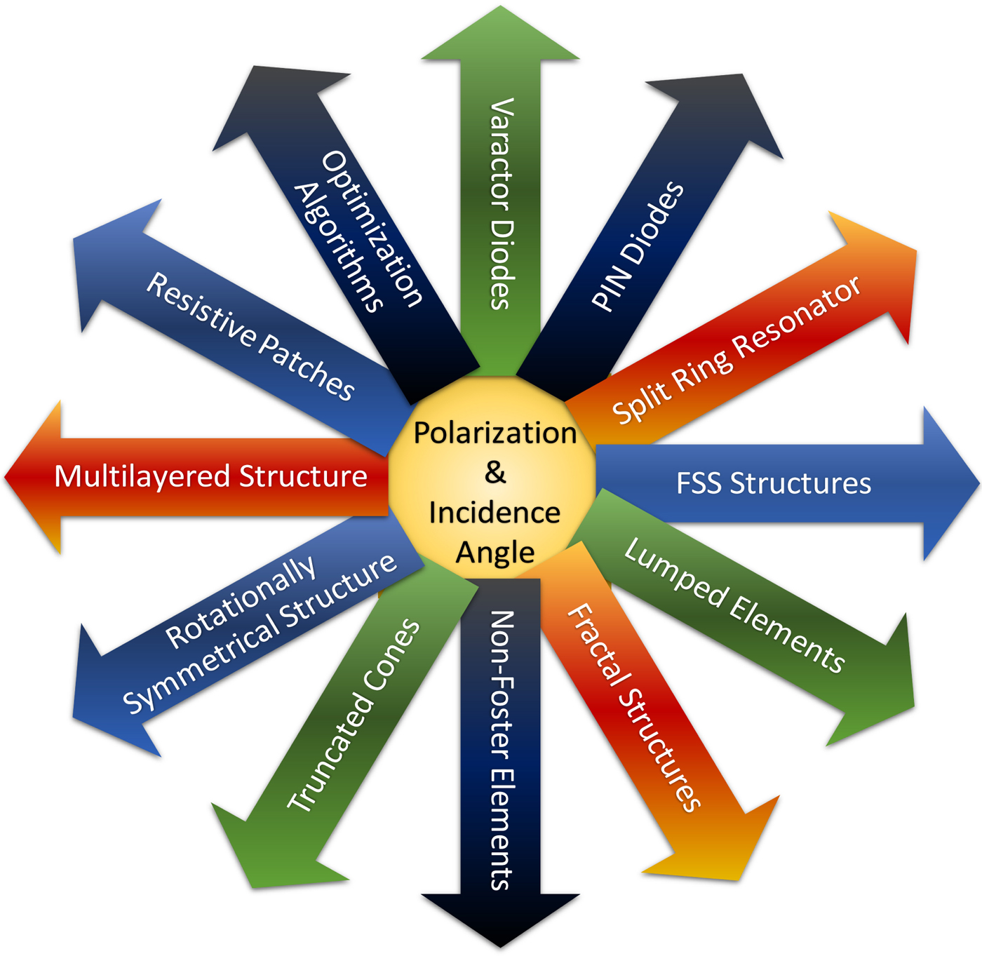
Figure 9 illustrates some popular techniques to overcome the issues of polarization and incident angle of EAs. The techniques to overcome the challenge of implementing the MA with perfect absorption along with incident angle and polarization insensitivity mostly focus on the utilization of two-dimensional patterns such as disks [Reference Liu, Mesch, Weiss, Hentschel and Giessen83], rings [Reference Nguyen, Bui, Nguyen, Nguyen, Lee, Nguyen and Vu84], circular holes [Reference Chaurasiya, Ghosh, Bhattacharyya and Srivastava85], and cross arrays [Reference Kong, Li, Jin, Ma, Zhang and Zhang86]. However, such designs have a disadvantage of restricted extension of the absorption band due to the limited number of resonances that are combined for wideband absorption. Recently, thin absorber using metallic/dielectric multilayered frustum pyramid and sawtooth structures are proposed for broadband absorption [Reference Lee, Ji and Guo87]. However, the structure exhibits incident angle insensitivity below 40° due to its low-level symmetrical structures. To examine the influence of incidence angle on absorption properties of the broadband absorber with multilayered symmetrical structures, Hoa et al. reported the broadband microwave MA based on a periodic arrangement of metallic/dielectric multilayered conical frustums [Reference Thi Quynh Hoa, Huu Lam and Duy Tung88]. The MA exhibits a perfect absorption with a wide angle of tolerance and polarization insensitivity due to its rotational symmetrical structure. Therefore, it is necessary to develop a perfectly symmetrical structure for broadband absorption of the MA which can improve the angle and polarization insensitivity. Besides the EAs, the characteristic of polarization insensitivity is essential for other EM applications also. Several researchers have implemented various PIAs. It has been found that broadband absorption is insensitive to the angles of incidence of TE and TM polarized waves and is dependent on the degree of symmetry of the structural design. Hence, PIAs are typically designed by using highly symmetrical structures such as rotational structure [Reference Seman and Cahill89], four-fold symmetrical structure [Reference Zhao, Cheng, Chen, Qi, Jiang and Cui90], or higher order symmetrical structures [Reference Li, Gao, Cao, Li, Zhang and Zhang91]. Such highly symmetrical structures are beneficial for implementing PIAs because the unit cell of the structure can resonate identically for distinct polarizations of the incident EM waves. Furthermore, it is important to note that most of the EAs can absorb the incident waves only on the top layer of the absorber. However, the bottom layer does not provide any absorption capability due to the metallic ground plane. The absorbers which do not have a bottom ground plane also suffer from bi-anisotropic effects [Reference Serdiukov, Semchenko, Tertyakov and Sihvola92] and interrupt the symmetry of the structure. This results in asymmetric absorption and causes degraded performance of the absorber. All electrically thin EAs suffer from asymmetric absorption due to the bi-anisotropic effect. Therefore, symmetric absorption of thin EAs can be accomplished by avoiding bi-anisotropic coupling among the layers of the absorber [Reference Ra'di, Asadchy and Tretyakov93]. The basic theory behind the symmetric absorption of the EM waves is that the structure should have the same electric and magnetic properties. Also, the electric and magnetic responses should resonate at the same resonant frequency.
Techniques to overcome the issues of polarization and incident angle of EAs.
Zhao et al. implemented a PIA using varactor diodes situated systematically on orthogonally deposited patterns [Reference Zhao, Cheng, Chen, Qi, Jiang and Cui90]. The structure is designed in such a way that the unit cell possesses 4-axial symmetry. Due to the symmetrical configuration, different resonators resonate in separate directions for distinct polarizations of the incident EM waves. Such configurations successfully refrain shorting of different resonating portions of the structure and provide tunable characteristics. Wu et al. designed a broadband PIA using MM with wide angle and near unity absorption for microwave frequencies [Reference Wu, Liu, Yu, Chen, Ma, Li, Li and Ye94]. The structure is composed of eight-fold rotationally symmetric SRRs as shown in Fig. 10. The wideband characteristic is achieved by arranging different resonators vertically and utilizing their coupling effect. The insensitivity to polarization and incident angles is achieved by the highly symmetrical arrangement of the structure in this case.
Geometrical representation of the unit cell of broadband MA using eight-fold rotationally symmetric SRR for wide angle ranges and polarization insensitivity. This figure is reproduced with permission from [Reference Wu, Liu, Yu, Chen, Ma, Li, Li and Ye94]. ©2016, Elsevier.

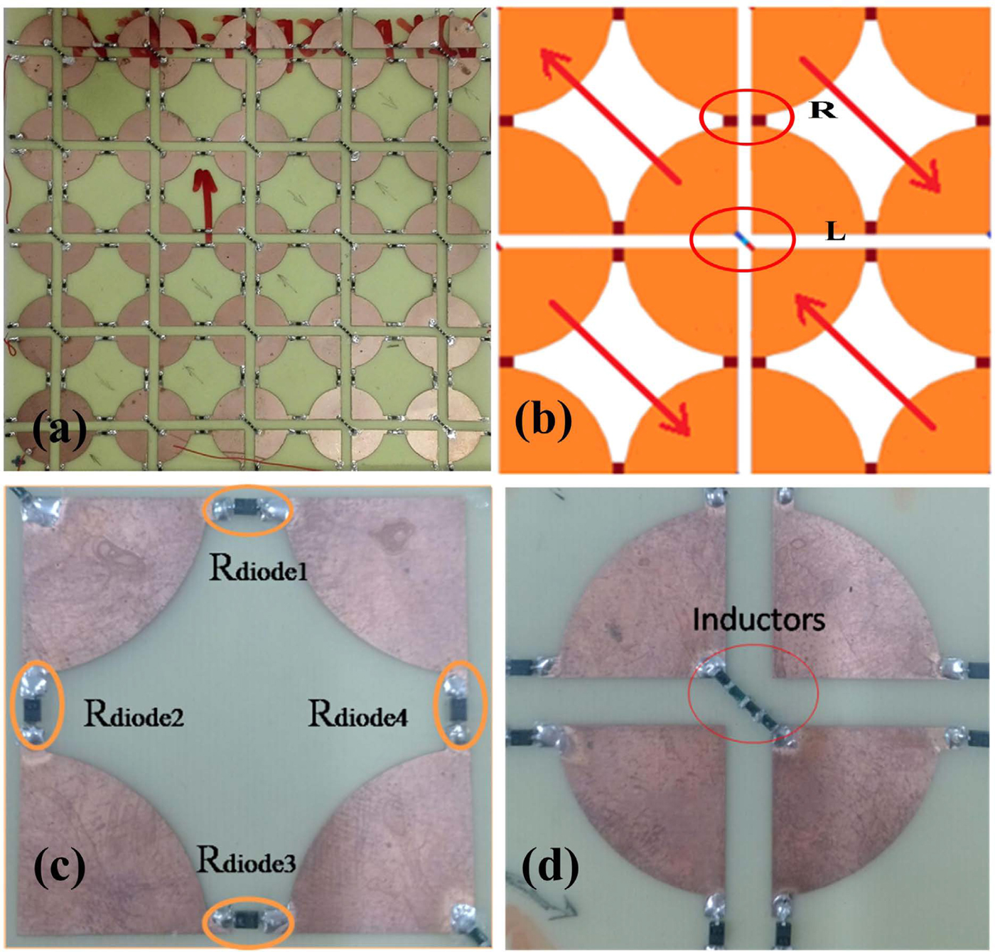
Wang et al. demonstrated an innovative tunable PIA using FSS [Reference Wang, Kong, Cheng, Bao, Yu, Miao and Jiang38]. The structure is composed of a periodic arrangement of PIN diodes and inductors as biasing lines as shown in Fig. 11. This structure also possesses 4-axial symmetry. The switchable behavior of PIN diode provides tunable characteristics, and the complete structure is capable of enhancing the necessary parameters of the PIA especially for the low-frequency band. The realization of tunable PIAs for wideband absorption is possible by using adjustable devices. Ghosh et al. realized an active FSS based PIA with switchable performance between single-band and wideband absorption [Reference Ghosh and Srivastava95]. The structure is composed of a periodic arrangement of square loops along with PIN diodes to provide switchable feature using a biasing network. The biasing network is responsible for the proper delivery of the bias voltage to all switchable components without interfering the normal resonance of the device. The polarization insensitivity for all angles is achieved by the 4-axial symmetrical design of the structure. The broadband absorption in C band is accomplished by the use of surface mounted resistors.
Experimental representation of tunable PIA using FSS and PIN diodes for large scan angles, polarization insensitivity, and bandwidth enhancement (a) fabricated prototype; (b) diagram of current flows; (c,d) magnified photos of the pattern. This figure is reproduced with permission from [Reference Wang, Kong, Cheng, Bao, Yu, Miao and Jiang38]. ©2016, Nature Publishing Group.
He et al. proposed an adjustable PIA based on an FSS for both C and X band applications [Reference He, Jiang, Chen, Li, Miao and Bie96]. The design using a symmetrical fan-shaped pattern significantly reduces the sensitivity to different polarizations of normally incident EM waves. Also, the reflectivity curves for the TM mode have the same absorption performance as that of the TE mode. PIN diodes connected between patterned unit cells help in achieving adjustability. By incorporating inductors into the metal patterns, an S-shaped series bias provides the bias voltage to PIN diodes. By tuning the working states of the diodes, an adjustable absorption performance from 4.6 to 13 GHz is achieved for both TE and TM polarizations at normal incidence of the EM waves. Here, the biasing lines not only provide the bias voltage for the PIN diodes to obtain an adjustable absorption performance but also helps in maintaining the polarization independence of the absorber. However, as the absorption performance under oblique incidence is considered for both polarization modes, the absorption bandwidth becomes narrower, and the amplitude of the reflectivity weakens. This explains that obliquely incident EM waves can change the absorber characteristics.
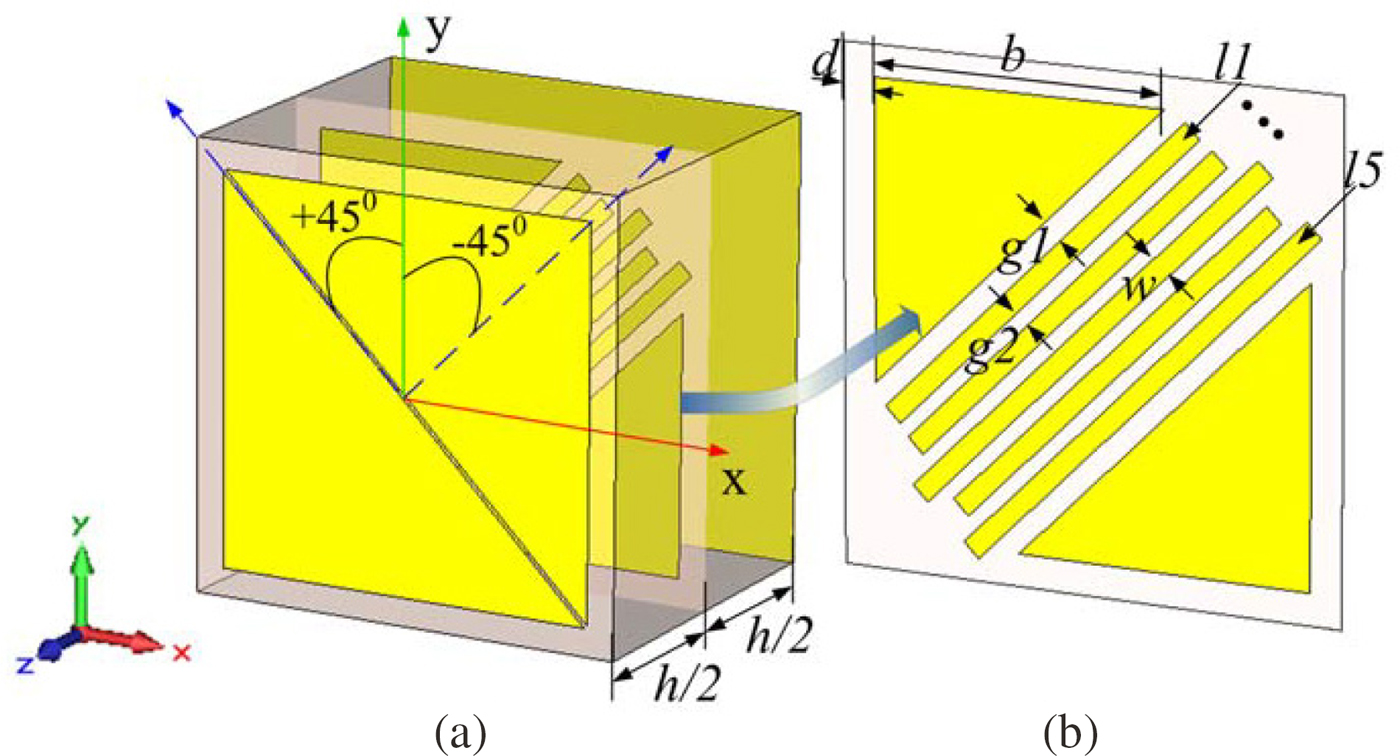
Cross-polarized reflection, though essential for linear reflective polarization converters, is undesired for the EAs. If the cross-polarization reflection from a surface is high, a linearly polarized incident EM wave gets reflected with its orthogonal polarization, rather than absorption of the incident waves. Cross-polarized reflection arises if the geometry of the unit cell is anisotropic [Reference Lin, Wang, Meng, Da, Li, Fang and Zhu97]. Advanced radar systems can easily detect, the cross-polarized reflection [Reference Knott and Senior98]. Therefore, the cross-polarized reflection must be reduced in an efficient absorber. When the lossy substrate is replaced by a lossless substrate, the absorption is reduced significantly. With high cross-polarized reflection, the contribution of losses to the total absorption is very less. The only part of reflected power, which is not converted to orthogonal polarization is absorbed by the loss components. If a lossless substrate is used, most of the incident power is reflected with cross-polarization. Thus, reduction of cross-polarized reflection from a periodic arrangement of the metal-backed anisotropic module may be an alternative approach to achieve compact and ultrathin absorber with broad bandwidth. In [Reference Kundu, Mohan and Chakrabarty99], cross-polarized reflection from a periodic array of metal-backed anisotropic units is reduced to achieve a compact ultrathin EA. Using an FSS as a middle layer, the peak absorptivity is improved from 23.75% to 73.45%, while its thickness and full width at half maxima (FWHM) bandwidth are kept unaltered. The structure is composed of two mutually perpendicular symmetric axes along ± 45° with respect to the y-axis as shown in Fig. 12. Therefore, the unit cell is anisotropic, and cross-polarized reflection is inevitably high. The structure resonates similarly for both TE and TM incidence as they are symmetrical for both the polarizations because of their diagonal arrangement.
Geometrical representation of (a) Unit cell and (b) Middle FSS layer of the absorber for reduction of cross polarization reflection. This figure is reproduced with permission from [Reference Kundu, Mohan and Chakrabarty99]. ©2017, John Wiley and Sons.
Fan et al. presented an active broadband MA design using non-Foster elements for microwave applications [Reference Fan, Zhang, Yin, Xu, Nagarkoti, Hao and Cui100]. They utilize an analytical circuit model to interpret the losses present in the material for oblique incidence of TE and TM polarized waves. The broadband absorption is accomplished by using active non-Foster components in association with this circuit model. These active components are realized by implementing a non-Foster circuit using tunnel diodes. The absorber also possesses wide-angle performance for an angle of incidence up to 45° for both TE and TM modes. In [Reference Chen, Hu, Wang, Huang, Wang, Hu and Liu49], a wideband absorber using HIS is reported which can absorb more than 75% of the incident radiation for up to 60° angle of incidence. It has been observed that the absorption rate and working bandwidth are inversely proportional to the angle of the incident EM waves. Since the resistive layer of the absorber is orthogonal to the electric field and parallel to the magnetic field, the absorptivity and working bandwidth in the TM mode drops significantly, higher than that in the TE mode. This causes a reduction in losses in the resistive layer. The structure provides broadband absorption of 90% of normally incident waves, but the absorption becomes progressively worse with the increase in incidence angle for both TE and TM polarized waves.
Kim et al. designed a MA using truncated cones in a multilayered structure and achieved two different working bands [Reference Kim, Yoo, Kim, Rhee, Kim and Lee101]. Both bands are wide and provide absorption up to 45° angle of incidence and insensitivity to polarization. However, the structure is complex, and multilayering causes a significant increase in the thickness of the absorber. Shen et al. accomplished an origami-inspired 3D MA with the broadband absorption of obliquely incident EM waves up to 75° of wide acceptable angles [Reference Shen, Pang, Wang, Ma, Pei and Qu102]. The 3D structure is implemented through the use of a periodical arrangement of folded resistive patches which results in increased absorption capability. They showed that an array of the folded resistive patch is capable of enhancing the working bandwidth of the absorber with the rise in the angle of incidence of the obliquely incident TM waves. It is important to note that the oblique incidence of the EM waves causes two common issues. One is the mismatching problem, and other is the upward movement of the center frequency. Both the issues are highly influenced by oblique incidences which significantly deteriorates the absorption properties of the absorbers. Coupling effect is an essential topic for oblique incidences. It causes higher absorption of normally incident waves than that of the obliquely incident waves [Reference Li, Gao, Cao and Zheng103]. Ayop et al. achieved absorption of incident waves with 69° of large oblique angles with a dual-band MA [Reference Ayop, Rahim, Murad and Samsuri104]. The structure is composed of two circular rings. However, the second band shows a significantly inferior absorption capability. Recently, the same team presented a dual-band MA for X band application [Reference Ayop, Rahim, Murad, Samsuri, Zubir and Majid105]. The structure is composed of a rectangular ring, a cross, and a slotted cross design and is very simple and symmetrical. They accomplished remarkable absorption at both working bands with very large incidence angles of more than 77° with polarization independence.
Prospects of Technologies in Flexible Absorbers Design
In the past few years, researchers made a tremendous amount of effort to explore the application of nanotechnology in the field of science and engineering. As a result, numerous promising solutions have been found for several scientific and engineering problems. Nanotechnology, also termed as the molecular manufacturing, is the study and realization of microscopic structures of the order of 1–100 nm which has given rise to the realization of numerous innovative materials and devices for various industrial applications. By manipulating a material at the nanoscale, the material properties can easily be tailored to achieve desired electron transport characteristics [Reference D'Amore, Sarto, Hanson, Naeemi and Tay106]. It is reported that use of the nano-materials in the field of the microwave absorbers has shown extended properties for the specific application by changing the fundamental constituents [Reference Najim, Smitha, Agarwala and Singh62]. The nano-particles have a larger surface to volume ratio, and if nano-composites are used as an absorbing material, enhanced microwave absorption properties can be attained [Reference Najim, Modi, Mishra, Adelung, Singh and Agarwala107].
The MAs are usually very hard and inflexible due to their realization of solid and rigid dielectric materials, thus, restricting their practical implementation within planar structures only. FR-4 dielectric material [Reference Kim and Lee108] is one of the very common examples of the materials that result in such rigid absorbers. However, various other dielectrics used for the implementation of absorbers such as silicon [Reference Tao, Strikwerda, Fan, Padilla, Zhang and Averitt109], vanadium oxide [Reference Wen, Zhang, Yang, Chen, Long, Jing, Lin and Zhang110] etc. also result in rigid absorbers. Ultrathin and flexible EAs are always desirable and beneficial for practical applications. Flexible absorbers are possible to realize if the dielectric materials possess flexibility feature [Reference Iwaszczuk, Strikwerda, Fan, Zhang, Averitt and Jepsen111,Reference Singh, Korolev, Afsar and Sonkusale112]. Various civil and defense applications require mechanically flexible wideband absorbers with good absorption capability. Salisbury screen, FSS structures, and many MM-based absorbers have been investigated for ultrathin thickness, but they provide either narrow bandwidth or decreased absorption. Bandwidth enhancement using multiple resonances, the combination of MMs with FSS patterns, and utilization of the lumped components have also been realized. Unfortunately, such structures also fail to provide flexibility with excellent absorption properties due to their fabrication on PCB boards with metallic patterns.
The conventional metallic conductive layer can be replaced by conductive inks to provide flexibility in the structure. Such inks possess magnificent advantages as compared with generally used metallic layers. These inks are obviously very light, thus, providing a light-weight feature. Mass production with rapid manufacturing process is one of the remarkable features of such printable inks for practical implementations via printed electronics. Inks with high conductivity are highly recommended for printing because the printing properties can be enhanced with the addition of non-conductive additives. These add-ons can be used to provide extended features such as waterproofing capability, extra adherence, increased endurance, and so on [Reference Kamyshny and Magdassi113]. Therefore, conductive polymers [Reference Cochrane, Koncar, Lewandowski and Dufour114], silver nanoparticles [Reference Layani and Magdassi115], silver nanowires (AgNWs) [Reference De, Higgins, Lyons, Doherty, Nirmalraj, Blau, Boland and Coleman116], copper nanowires [Reference Rathmell and Wiley117], carbon nanotubes [Reference Hu, Hecht and Gruner118], graphene [Reference Geim and Novoselov119], and other conductive nanomaterials have been investigated for implementing printable absorbers with enhanced features. However, inks using the silver nanoparticles are found to be considerably expensive, and they provide low fabrication efficiency. The AgNWs have much higher aspect ratios (relatively more than 700) and are much more reliable for controlling their surface resistance. The copper nanoparticles are considerably low-cost inks, but they are easily oxidizable at higher temperatures. Oxidization of the carbon nanotubes is relatively tough, and they are economically good. The conductive polymers are thermally and chemically unreliable and possess inferior conductivity than that of the silver/carbon nanoparticles. Graphenes are thermally reliable and possess superior electron mobility, conductivity, and tunability. Several EAs have been developed using the properties of graphene such as electrically switchable absorbers [Reference Balci, Polat, Kakenov and Kocabas120], tunable wideband absorbers [Reference Huang, Hu and Liu121], THz absorbers [Reference Huang, Zhang, Hu, Aqeeli and Alburaikan122], flexible radar absorbers [Reference Huang, Pan and Hu123] etc. However, graphene-based absorbers require costly manufacturing process. Therefore, graphene nano-flakes inks are used as a good alternative enabling economic mass production feature.
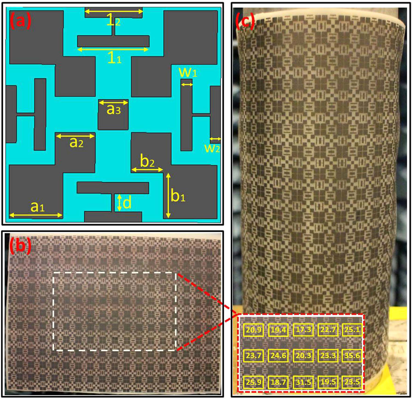
Kim et al. proposed a flexible MA especially for cylindrical devices using printing technology [Reference Kim, Ling, Kim and Lim124]. Silver nanoparticle ink is used as conductive coating due to their superior conductive characteristics. The ink is applied in a flexible polymer film by ink jetting them through an inkjet printer. The MA provides flexibility and more than 95% absorptivity at 9.21 GHz for flat as well as a cylindrical surface having a diameter of 9.12 cm for all polarizations up to 30° of oblique angles on a 0.62 mm thick substrate. Lee et al. presented a MA implemented on an ordinary textile by the screen printing technique using silver conductive ink for wearable devices [Reference Lee, Kim and Lim125]. The unit cell of the structure comprises a Chanel logo at the top and copper tape as the ground plane as shown in Fig. 13. There is no transmitted wave because of the bottom copper tape, which effectively restricts incident waves to pass through it. The absorber can absorb almost perfectly at 10.8 GHz under normal incidence, with only 1.2 mm thickness. As a result, they demonstrated the possibility of integrating the wearable technology with MM-based absorbers using the screen printing technology. Since the absorber is implemented by using the screen printing method, it is simple, fast, and suitable for mass production. Yoo et al. realized a MA on a flexible paper with silver nanoparticle inks for X band applications [Reference Yoo, Kim, Kim, Tentzeris and Lim126]. Flexibility is achieved through inkjet printing of the conductive design with the silver nanoparticle inks on a flexible paper as a dielectric material. The structure comprised modified JCR with a conductive ground plane. The MA is implemented by inkjet printing technique on a flexible paper substrate. Such absorbers do not yield any chemical squander due to the eco-friendly behavior of papers. The structure is designed in such a way that it is angularly independent and works very well for both plain as well as cylindrical surfaces. The MA can absorb more than 95% of the incident waves at 9.09 GHz for all polarizations up to 40° of oblique angles in a 1.19 mm thick structure.
Experimental representation of screen printed flexible MA and its magnified unit cells implemented on an ordinary textile for wearable application. This figure is reproduced with permission from [Reference Lee, Kim and Lim125]. ©2017, John Wiley and Sons.

Huang et al. realized a flexible and broadband MA using graphene nano-flakes inks for radar applications [Reference Huang, Pan and Hu123] as shown in Fig. 14. The graphene conductive ink is used to print an FSS design on the top of a flexible silicon dielectric material through stencil printing technique. The ground plane of the absorber is entirely conductive. The absorber provides an excellent Radar Cross Section (RCS) reduction at both X and Ku bands for planar as well as cylindrical surfaces. The MA can absorb more than 90% of the incident waves from 10.4 to 19.7 GHz only on 2 mm thick structure with a fractional bandwidth of 62%. Kim et al. proposed straightforward design equations for realizing a wideband EA at some specific resonant frequency [Reference Kim and Lee136]. They observed that a series RLC resonant unit is capable of modeling the impedance of resistive dipoles. Therefore, they used crossed dipoles with chip resistors as RLC screens for the implementation of the broadband absorber. They achieved near perfect absorption of normally incident waves at 10.93 GHz with polarization insensitivity on a 3.2 mm thick absorber. However, chip resistors restrict the mass production of the absorber due to the time-consuming manufacturing process.
Unit cell structure and experimental representation of printed graphene nano-flakes radar absorber for flexibility and broadband absorption from X to Ku band. This figure is reproduced with permission from [Reference Huang, Pan and Hu123]. ©2016, Nature Publishing Group.
Lee et al. proposed a wideband EA using AgNW resistive film for X band applications [Reference Lee and Lee131]. The structure is very light because of the use of cross-shaped resistive AgNW film at the top of a styrofoam dielectric material with a conducting ground plane. The EA can absorb more than 80% of the incident waves from 6 to 14 GHz for all polarizations in a 7.5 mm thick substrate with 90% absorption bandwidth. This absorber has the advantage of being cost-effective and the possibility of mass production with the assistance of laser cutting machines.
A comparative collection of recently reported wideband EM absorbers for microwave applications is listed in Table 2. It compares the simulated absorptivity, frequency range, bandwidth, polarization dependence, angle of incidence and thickness of the EAs because this review mainly focuses on these five parameters of the absorbers. The comparative study is presented in descending order of the absorption bandwidth to provide a more precise view as a reference to the broadband behavior of the absorber and to justify the need for perfect economical microwave thin absorbing material to achieve absorption over a wide range of frequencies of interest.
List of recently reported broadband microwave absorbers with their absorptivity, polarization, incidence angle, and thickness (Arranged in descending order of the bandwidth of the absorbers)

Applications
There are a variety of applications of the EAs used for various purposes at different frequency bands of the EM spectrum. Although initially absorbers were meant for camouflage and improvement of radar performance, they established their existence into numerous diverse areas. This section provides a list of the several possible applications of the EAs used in various civilian and defense sectors. The most promising use of the absorbers are in the field of defense and aeronautics, where they are employed in stealth technology [Reference Chen, Hu, Wang, Huang, Wang, Hu and Liu49,Reference He, Jiang, Chen, Li, Miao and Bie96,Reference Bu, Yue, Zhang, Hu and Dong128], RCS reduction [Reference Sun, Gu, Chen, Li, Liu, Xu and Zhou36,Reference Kim, Lee and Lim73,Reference Huang, Pan and Hu123,Reference Ozden, Yucedag and Kocer135], and radar absorbing materials [Reference Kundu, Mohan and Chakrabarty99]. The emerging technology in the field of material science has played a very important role in realizing the polymer based materials inherently used as radar absorbing materials for RCS reduction in stealth technology. These materials have a larger lifespan along with low weight and can be easily applied on the surface of aerospace vehicles. Absorbers play an important role in acquiring a low RCS of antennas [Reference Li, Zhang, Fu and Yuan137]. Moreover, they can also be used to increase the RCS. To improve the detectability and effectiveness of a missile decoy, its rear side is coated with absorbers which increases its radar signature by reducing the creeping waves [Reference Harrington138]. Absorbing layers are also utilized to shield objects residing in the neighborhood of the radar systems to improve its performance [Reference Emerson139].
The RF anechoic chambers are designed in such a way that it can completely absorb EM waves and its reflections by covering the interior surfaces (walls, floor, and ceiling) of the chamber with radiation absorbent materials to simulate a free space environment. Majority of such chambers incorporate pyramidal, conical, or sine wave shaped absorbers [Reference Emerson139]. Other areas of applications of EAs are in the field of consumer and industrial electronics where they are used for the mitigation of EMI [Reference Ahmadia and Idab130], enhancement of EM compatibility [Reference Yoo, Ju, Park, Kim, Bong, Lim, Kim, Rhee and Lee79] of the devices, subsystems, and systems as well as in EM shielding technology [Reference Munaga, Ghosh, Bhattacharyya and Srivastava19,Reference Wang, Kong, Cheng, Bao, Yu, Miao and Jiang38]. Electronic circuits and devices that operate at higher frequencies are a major source of EM radiation and require the use of suitable shielding solutions to prevent spurious radiations arising either from its own components and circuitry or from the nearby systems and devices. Absorbers are essential for diminishing the mutual coupling of closely placed antennas [Reference Channabasappa and Egri140], mitigating the harmful effects of cavity resonance in enclosed monolithic microwave integrated circuits (MMIC) [Reference Dyczij-Edlinger, Kingsland, Peng, Perepelitsa, Polstyanko and Lee141], alleviating the effect of apertures in metallic cavities and attenuating surface waves. A variety of customized absorbers are used to ensure proper EMI level for diverse high-frequency devices and applications.
Other applications where they are used extensively are imaging [Reference Ghosh and Srivastava95], phase imaging [Reference Ghosh, Bhattacharyya, Chaurasiya and Srivastava134], medical imaging [Reference Montaser20], and thermal imaging. Most of these imaging techniques employ MAs in their imaging systems to control the EM process such as absorption, polarization, and spectral bandwidth. Selective multi-frequency sensor [Reference Asadchy, Faniayeu, Ra'Di, Khakhomov, Semchenko and Tretyakov81], healthcare sensor [Reference Lee, Kim and Lim125], thermal sensor [Reference Sen, Islam, Banerjee and Das129], plasmonic sensor etc. also employ absorbers. The susceptibility of the MM to environmental influences causes the shift in resonant frequency which facilitates the detection of the change in the physical parameters such as pressure, density, dielectric constant etc. These sensors employing MAs have low cost, low loss, high sensitivity and resolution apart from durability. The energy harvesting technology uses properly designed absorbers in the design of solar cell [Reference Wu, Liu, Yu, Chen, Ma, Li, Li and Ye94]. The EAs also enhance the solar energy collection [Reference Long, Yin, Wang, Li, Zhu and Guan61] due to its high absorptivity. The photovoltaic solar cells [Reference Zhang, Cheng, Yang, Zhao and Cui75] also invariably make use of absorbers. The detection of EM energy is facilitated by polarization detectors and ultrathin photodetectors employing the absorbers.
There are a wide variety of microwave components such as filters [Reference Asadchy, Faniayeu, Ra'Di, Khakhomov, Semchenko and Tretyakov81], bolometers [Reference Landy, Sajuyigbe, Mock, Smith and Padilla21], thermal emitter [Reference Liu, Tyler, Starr, Starr, Jokerst and Padilla9], amplifier [Reference Hamm, Wuestner, Tsakmakidis and Hess12], switches [Reference Hajizadegan, Ahmadi and Sakhdari13] etc. that make use of absorbers. Resistive vanes made with absorbing materials are exploited for the manufacturing of microwave attenuators and phase shifters. Absorbers also provide necessary harmonic suppression in transmitters, and gain stabilization in amplifiers. Absorbers are also employed in televisions to remove the ghost images occurring due to clutter effects from nearby buildings [Reference Kim, Kim, Jung and Song142]. Microwave absorbers also find its use as protective shields in microwave ovens to suppress any spurious leakage from the oven to the outside environment [Reference Ishino, Hashimoto and Abe143]. Many antennas exhibit high sidelobe levels which can be minimized to the desired level by covering the antenna with a panel of suitable absorbers [Reference Yokoi and Fukumuro144]. Such an arrangement of suitable absorbers can also eliminate the obstructions arising from the feeding supports of reflector antennas. Similarly, placing an absorbing material at the edges of large reflector antenna can reduce the effects of edge diffraction.
In the area of wireless communication, the absorbers play a significant role in wearable devices [134], UHF-RFID systems [Reference Zuo, Yang, He, Zhan and Zhang145], 4G communications [Reference Zuo, Yang, He, Mao and Liu55], satellite communication, long distance radio telecommunications and high-speed wireless communication [Reference Namai, Sakurai, Nakajima, Suemoto, Matsumoto, Goto, Sasaki and Ohkoshi146], cordless telephones, cell phones [Reference Pretorius147], Wi-Fi devices [Reference Montaser20], where they are mainly used for the purpose of absorbing the radiation in the undesired direction so that the devices can be made safer for the human being and provide high-quality communication.
Conclusion
This review brings together various challenging aspects encountered in designing a low-cost thin, perfect EA for achieving wide absorption bandwidth and good absorption properties such as polarization-insensitivity, wide incident angle, and near perfect absorption. Some basic concepts, theories, properties, and needs of the EAs are discussed along with historical accomplishments. Various complications related to the absorption bandwidth and the thickness of the EAs are also highlighted. The techniques for maximizing the working bandwidth and minimizing the thickness by utilizing highly absorbent materials, lumped circuit elements, high loss materials, resistive films or sheets, magnetic medium substrates, SSPPs, FAs, CAAs, water, and chiral bi-anisotropy are discussed. Other approaches of combining different resonant units horizontally or vertically, i.e., multilayering to overcome the constraint of wide bandwidth and least thickness are elaborated. The need of several optimization algorithms such as GA, ANN, PSO, etc. attempted to fulfill this purpose is also outlined. Further impacts of polarization and incidence angles are considered. Highly symmetrical structures with varactor diodes, PIN diodes, SRRs, FSS, lumped elements, fractal structures, non-Foster elements, rings, cross structures with slots, the multilayered structure, folded resistive patches, etc. are some of the recent research trends to withstand the issues of polarization and incidence angles. Several prospects of nanotechnology in absorber design are also reviewed. Benefits and limitations of conductive polymers, silver nanoparticles, AgNW, copper nanowires, carbon nanotubes, graphene are discussed for implementing printable absorbers with enhanced features. Finally, several possible applications of EAs used in various civilian and defense sectors are presented. A challenge to realize a low cost, thin, and perfect absorber which can simultaneously satisfy multiple constraints such as wide-angle, polarization-independence, and broadband absorption is still ahead.
Author ORCIDs
Manish Mathew Tirkey 0000-0001-8055-9223
 Manish Mathew Tirkey was born in Ranchi, India in 1991. He received the Master's degree in Electronics and Communication Engineering from Birla Institute of Technology, Mesra, Ranchi, India in 2016 and he is currently pursuing Ph.D. in Electronics and Communication Engineering from the same Institute. His scientific interests involve Electromagnetic Theory, Antennas & Wave Propagation, Electromagnetic Compatibility, and Metamaterial & its applications. His current research is focused on the investigation of various aspects of perfect Electromagnetic Wave Absorber.
 Nisha Gupta received the Bachelor's and Master's degrees in Electronics and Telecommunication and Electrical and Electronics engineering both from Birla Institute of Technology, Mesra, Ranchi, India and the Ph.D. degree from the Indian Institute of Technology, Kharagpur, India. She was a post-doctoral fellow at University of Manitoba, Canada from 1997 to 1998 before joining the Department of Electronics and Communication Engineering, Birla Institute of Technology in 1999 as a Reader. Currently, she is a Professor in the same department. She has authored and co-authored more than 100 technical journal articles and conference papers. Her research interests are Computational Electromagnetics, Antennas for Wireless Communication, AI techniques in Wireless and Mobile Communication, and EMI/EMC.


