


Introduction
Thin-film magnetoelectric (ME) composites are attractive candidates for use in biomagnetic sensors, energy harvesters [Reference Yarar, Fichtner, Hayes, Piorra, Reimer, Lisec, Frank, Wagner, Lofink, Meyners and Quandt1], highly efficient power converters, magnetometers, RF tunable inductors, and mechanical antennas [Reference Leung, Li, Viehland and Zhuang2, Reference Tu, Chu, Spetzler, Hayes, Dong, Liang, Chen, He, Wei, Lisenkov, Lin, Lin, McCord, Faupel, Quandt and Sun3, Reference Srinivasan, Priya and Sun4, Reference Xi, Qian, Lu, Mei, Rupprecht, Yang and Zhang5]. Heterostructures with aluminum nitride (AlN) serving as the piezoelectric layer and amorphous iron-cobalt silicon boron (FeCoSiB) alloy as the magnetostrictive layer have demonstrated ME coefficients in vacuum as large as 20 kV/cm Oe [Reference Kirchhof, Krantz, Teliban, Jahns, Marauska, Wagner, Knöchel, Gerken, Meyners and Quandt6] with limits of detection as low as  ${{1\;{\rm{pT}}} / {\sqrt {{\rm{Hz}}} }}$ [Reference Kirchhof, Krantz, Teliban, Jahns, Marauska, Wagner, Knöchel, Gerken, Meyners and Quandt6, Reference Tong, Yang, Guo, Li, Ouyang, Lin and Chen7, Reference Röbisch, Salzer, Urs, Reermann, Yarar, Piorra, Kirchhof, Lage, Höft and Schmidt8]. The ME voltage and sensitivity can be enhanced by 1–2 orders of magnitude when driven at the mechanical resonant frequency [Reference Tu, Chu, Spetzler, Hayes, Dong, Liang, Chen, He, Wei, Lisenkov, Lin, Lin, McCord, Faupel, Quandt and Sun3, Reference Jahns, Piorra, Lage, Kirchhof, Meyners, Gugat, Krantz, Gerken, Knöchel and Quandt9, Reference Zhao, Zhao, Hunter, Suchoski, Gao, Mathews, Wuttig and Takeuchi10]; therefore, many applications could benefit from a ME composite with a tunable resonant frequency. For example, deep brain stimulation (DBS) is a medical treatment used on patients suffering from tremors or dystonia. In this treatment, an array of electrodes are implanted deep in the patient's brain and stimulated at a well-defined frequency between 130 and 170 Hz [Reference Deuschl and Agid11]. For localization of the stimulated area near the electrode, it would be necessary to precisely tune the mechanical resonant frequency of a ME sensor to match the stimulation frequency of the electrode, or one of its multiples [Reference Deuschl and Agid11, 12, Reference Schuepbach, Rau, Knudsen, Volkmann, Krack, Timmermann, Hälbig, Hesekamp, Navarro, Meier, Falk, Mehdorn, Paschen, Maarouf, Barbe, Fink, Kupsch, Gruber, Schneider, Seigneuret, Kistner, Chaynes, Ory-Magne, Brefel Courbon, Vesper, Schnitzler, Wojtecki, Houeto, Bataille, Maltête, Damier, Raoul, Sixel-Doering, Hellwig, Gharabaghi, Krüger, Pinsker, Amtage, Régis, Witjas, Thobois, Mertens, Kloss, Hartmann, Oertel, Post, Speelman, Agid, Schade-Brittinger and Deuschl13].
Nickel–titanium (NiTi) shape memory alloys (SMA) can reversibly undergo a diffusion-less solid-to-solid phase transformation among the martensite phase (monoclinic), austenite phase (cubic), and R-phase (rhombohedral). The Young's modulus of the high-temperature austenite phase is usually larger than that of the low-temperature martensite phase [14]. To change the resonant frequency of a ME sensor, Röbisch et al. [Reference Röbisch, Piorra, de Miranda, Quandt and Meyners15] proposed harnessing the reversible and gradual change in the Young's modulus of NiTi SMA substrates [Reference Röbisch, Piorra, de Miranda, Quandt and Meyners15]. The entire 2.5 × 15 mm SMA/ME composite (1 μm AlN/2 μm FeCoSiB/50 μm NiTi) was annealed at 450 °C for 30 min, to crystallize the NiTi layer. Progressive heating and cooling of this AlN/FeCoSiB/NiTi cantilever induced the reversible phase transformation in the SMA, resulting in a mechanical resonant frequency shift (Δf) of 12%. Below room temperature, at T = 20 °C, the SMA was in the martensite phase with f martensite = 332 Hz. Heating the SMA to T = 130 °C induced the phase transformation to the austenite phase with f austenite = 351 Hz. Finally, cooling the SMA to T = 64 °C induced another transition to the R-phase with a corresponding change in the resonant frequency to f R-phase = 312 Hz [Reference Röbisch, Piorra, de Miranda, Quandt and Meyners15]. Although varying the temperature was used to experimentally induce the phase transformation in this study, one could also control this transformation through the application of stress.
The martensitic transformation temperatures and fatigue stability of NiTi-based SMAs can be tuned for the desired application by alloying with elements such as Pt, Au, Cu, Hf, Co, and Pd [Reference Chluba, Ge, de Miranda, Strobel, Kienle, Quandt and Wuttig16, Reference Kohl, Dittmann, Quandt and Winzek17, Reference Vitushinsky, Schmitz and Ludwig18, Reference Quandt, Halene, Holleck, Feit, Kohl, Schloβmacher, Skokan and Skrobanck19]. In this manuscript, the alloy Ti50Ni35Cu15 is investigated because previously it was identified as an ultralow fatigue SMA material, able to undergo this phase transformation for millions of cycles, reversibly [Reference Chluba, Ge, de Miranda, Strobel, Kienle, Quandt and Wuttig16, Reference Gu, Bumke, Chluba, Quandt and James20]. The sputter deposition process we use results in thin-film amorphous SMAs; therefore, all samples must be crystallized at high temperatures (450–700 °C) to enable the martensitic phase transformation [Reference Fu, Huang, Du, Huang, Tan and Gao21]. The annealing process has a significant impact on the surface morphology of crystalline TiNiCu films, where higher postsputter annealing temperatures increase the surface roughness and grain size of TiNiCu [Reference Fu, Du, Zhang and Gu22]. The integration of high-quality AlN piezoelectric and TiNiCu SMA thin films is the key task for the future development of a ME sensor with a tunable resonant frequency. The major aim of the presented work was to evaluate the influence of the annealing TiNiCu on the piezoelectric performance of AlN in fabricated AlN/Pt/Ta/TiNiCu/Ta/Si/FeCoSiB composites.
Results and discussion
Analytical calculation of resonant frequency
Mechanical resonant frequencies are well studied for cantilever systems composed of a substrate and a thin film [Reference Röbisch, Piorra, de Miranda, Quandt and Meyners15, Reference Zannon23, Reference Whitney24]. The theory and Matlab code presented by Zannon et al. [Reference Zannon23] are adapted here to calculate the resonant frequency of a freestanding cantilever beam composed of three mechanically coupled thin-film layers (ME/NiTi/Si). The thick Si and NiTi substrates will dominate the elastic properties of the vibration; therefore, the contributions of the adhesion and electrode layers are neglected. The ME mechanical properties (E ME and ρME) are estimated in Eqs. (S1) and (S2) (Supplementary material I) using the thickness weighted average of the piezoelectric (2 μm AlN) and magnetostrictive (2 μm FeCoSiB) functional layers. Adding additional thin-film material layers to the composite will shift the center of mass (y cm) and inertia (I x) of the beam layers which can be calculated for using Eqs. (S3)–(S6) (Supplementary material I). Eq. (1) shows that the resonant frequency is dependent on the geometrical dimensions of the cantilever: width (w), length (L), and thickness (t x), as well as Young's modulus (E x), density (ρx), moment of inertia (I x), and in-plane surface area (A x) of each material layer (x = ME, NiTi, Si). λ is an integration constant determined by the boundary conditions for the first bending mode of a cantilever beam (λ = 1.875) [Reference Zhao, Zhao, Hunter, Suchoski, Gao, Mathews, Wuttig and Takeuchi10].
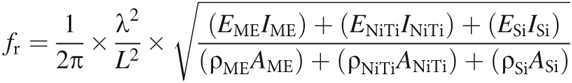 $${f_{\rm{r}}} = {1 \over {2\pi }} \times {{{\lambda ^2}} \over {{L^2}}} \times \sqrt {{{\left( {{E_{{\rm{ME}}}}{I_{{\rm{ME}}}}} \right) + \left( {{E_{{\rm{NiTi}}}}{I_{{\rm{NiTi}}}}} \right) + \left( {{E_{{\rm{Si}}}}{I_{{\rm{Si}}}}} \right)} \over {\left( {{\rho _{{\rm{ME}}}}{A_{{\rm{ME}}}}} \right) + \left( {{\rho _{{\rm{NiTi}}}}{A_{{\rm{NiTi}}}}} \right) + \left( {{\rho _{{\rm{Si}}}}{A_{{\rm{Si}}}}} \right)}}} \quad$$
The largest Young's modulus difference for NiTi occurs between the martensite phase (E Martensite = 28–41 GPa) and austenite phase (E Austenite = 41–83 GPa) [Reference Šittner, Heller, Pilch, Curfs, Alonso and Favier25]. Therefore, the maximum Δf will occur when there is a full transformation from martensite to austenite, as shown in Eq. (2).
 $$\Delta f = \left( {{{\left( {{f_{{\rm{austenite}}}} - {f_{{\rm{martensite}}}}} \right)} / {{\rm{\ }}{f_{{\rm{austenite}}}}}}} \right)\; \times \;100\quad$$
The analytical calculations presented in this article use the standard literature values of sputtered thin-film binary NiTi [14] to generalize the resonant frequency calculation for other SMA (i.e., TiNiCu, TiNiCuCo, NiTiPd, and NiTiPt) because the mechanical properties of thin-film NiTi [Reference Fu, Huang, Du, Huang, Tan and Gao21, Reference Šittner, Heller, Pilch, Curfs, Alonso and Favier25] are similar to those of TiNiCu [Reference Gu, Bumke, Chluba, Quandt and James20]. A summary of all material properties used in the following calculations and experiments is shown in Table I.
Mechanical properties ME/SMA/Si composite used in analytical calculations.

ME sensors fabricated onto smooth Si and polycrystalline Si substrates are known to have large mechanical quality factors [Reference Zabel, Kirchhof, Yarar, Meyners, Quandt and Faupel26]. The mechanical resonant frequency of both the martensite and austenite phase is evaluated as a function of NiTi thickness on 350 μ and 100 μm thick Si substrates in Figs. 1(a) and 1(b), respectively. As the NiTi thicknesses increases, Δf also increases, due to a larger volume of material undergoing the phase transformation. However, due to the thick Si layers, only a small shift is theoretically achievable (Δf Si = 350μm = 0.1–2%) and (Δf Si = 100μm = 0.3–5.4%). As shown in Fig. 1(c), when the Si substrate is eliminated, Δf can be significantly enhanced (Δf freestanding = 7.6–28.3%). Without the Si substrate present, one must consider if the neutral plane [y cm, Eq. (S3)] were to lie within the AlN layer in the ME stack, then the sensor could lose its sensitivity due to a balance in compressive and tensile stresses, causing a loss of polarization of AlN [Reference Hong, Sui, Zhang and Shi27]. This would likely prevent the ME effect and must be considered when ME composites are fabricated onto freestanding SMA substrates.
Analytical calculation demonstrating resonant frequency dependence on NiTi thickness on (a) 350-µm-, (b) 100-µm-, and (c) 0-µm-thick Si substrates. The largest shift in resonant frequency (Δf) occurs when there is a full phase transformation from martensite (E m = E martensite = 41 GPa) to austenite (E a = E austenite = 83 GPa).

The validity of the analytical calculations was checked by obtaining an experimental resonant frequency measurement on a fabricated (2 μm AlN/5.1 μm TiNiCu/350 μm Si/2 μm FeCoSiB) ME composite at room temperature. Analytical calculations predicted a resonant frequency of 768 Hz in the martensite phase and 772 Hz in the austenite phase for a 2.5 × 25-mm cantilever ME composite of similar thicknesses. The experimental resonant frequency (f experiment = 771 Hz) is in close agreement with the calculated resonant frequency, as indicated by the green star in Fig. 1(a). These results are further discussed in the Supplementary material I.
SMA ME sensor fabrication
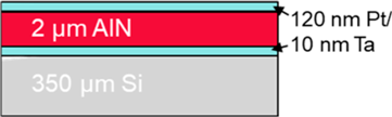
As depicted in Fig. 2, Pt/Ta/AlN/Pt/Ta/TiNiCu/Ta/Si/Ta/FeCoSiB/Ta composites were deposited via magnetron sputtering (Von Ardenne CS 730S) and structured through a combination photolithography (Karl Suss MA6), and wet and dry etching techniques. Starting with a 350-μm thick double-side polished (100) Si wafer [Fig. 2(a)], an adhesion layer (10 nm Ta) and amorphous SMA film (5.1 μm Ti55Ni30Cu15) are deposited [Fig. 2(b)]. Next, the piezoelectric component is formed into a parallel plate capacitor configuration through deposition of the adhesion layer (10 nm Ta), the bottom electrode (120 nm (111) Pt) [Fig. 2(c)], piezoelectric layer (2 μm AlN) [Fig. 2(d)], another adhesion layer (10 nm Ta), and the top electrode [120 nm (111) Pt] [Fig. 2(e)]. A (111) Pt orientation for the bottom electrode is critical to promote c-axis (002) AlN texture during the low-temperature pulsed DC reactive sputtering process used here [Reference Yarar, Hrkac, Zamponi, Piorra, Kienle and Quandt28]. The top electrode and AlN layer are structured using ion beam etching (IBE-Oxford Instruments Ionfab 300 IBE), and a wet etchant (85 wt% H3PO4, 80 °C) [Reference Yarar, Hrkac, Zamponi, Piorra, Kienle and Quandt28], respectively. Finally, the deposition of the amorphous phase magnetostrictive layer, sandwiched between an adhesion layer and protection layer (10 nm Ta/2 μm FeCoSiB/10 nm Ta), is executed via RF sputtering on the backside of the Si wafer and structured through photolithography and IBE as shown in Fig. 2(f). The annealing step required to crystallize the SMA must occur before magnetostrictive deposition because amorphous FeCoSiB is known to crystallize at temperatures above 300 °C [Reference Tong, Yang, Guo, Li, Ouyang, Lin and Chen7, Reference Hrkac, Lage, Köppel, Strobel, McCord, Quandt, Meyners and Kienle29]. An advantage to putting FeCoSiB on the backside is the Si substrate is providing a smooth surface for the deposition of FeCoSiB because previously it was shown to significantly improve the soft magnetic properties [Reference Yarar, Salzer, Hrkac, Piorra, Höft, Knöchel, Kienle and Quandt30, Reference Piorra, Jahns, Teliban, Gugat, Gerken, Knöchel and Quandt31]. The cross section of the fabricated device is shown in Fig. 2(g). The specific sputter parameters (pressure, power, Ar flow, etc.) of each material layer in the composite are given in Table SI (Supplementary material II).
Process flow for SMA/ME magnetoelectric composite fabrication. (a) Starting material 350-µm-thick Si. (b) Sputter deposition of amorphous 5-µm-thick TiNiCu*. (c) Deposit bottom electrode 120 nm (111) Pt. (d) Low-temperature pulsed DC reactive sputtering of piezoelectric layer 2 µm (002) AlN, structured via wet etching with H3PO4. (e) Deposit top electrode 120 nm (111) Pt, structured via ion beam etching*. (f) Deposit magnetostrictive layer 2 µm FeCoSiB, and structured via ion beam etching. (g) 2D cross section of final fabricated device. *Rapid thermal anneal (RTA) heat treatment to crystallize the SMA can occur either before step (b) or after step (e).

Polycrystalline sputtered AlN is able to withstand annealing temperatures of up to 1350 °C [Reference Evans, Liaw and Lin32]. The workflow offers two possibilities: crystallization of TiNiCu at 700 °C for 15 min by rapid thermal annealing (RTA, CreaTec Fischer and Co. GmBh) (i) before or (ii) after deposition of AlN, as reflected in steps (b) and (e) in Fig. 2. The annealing step is the most critical part of the process flow because it will set the SMA's microstructure which ultimately will determine the SMA's thermal and mechanical properties. In addition, the annealing temperature will control the martensitic transformation temperatures of the SMA [Reference Fu, Huang, Du, Huang, Tan and Gao21]. We only investigated an annealing temperature of 700 °C in this article; however, temperatures between 450 and 800 °C would be suitable for most NiTi-based SMA materials.
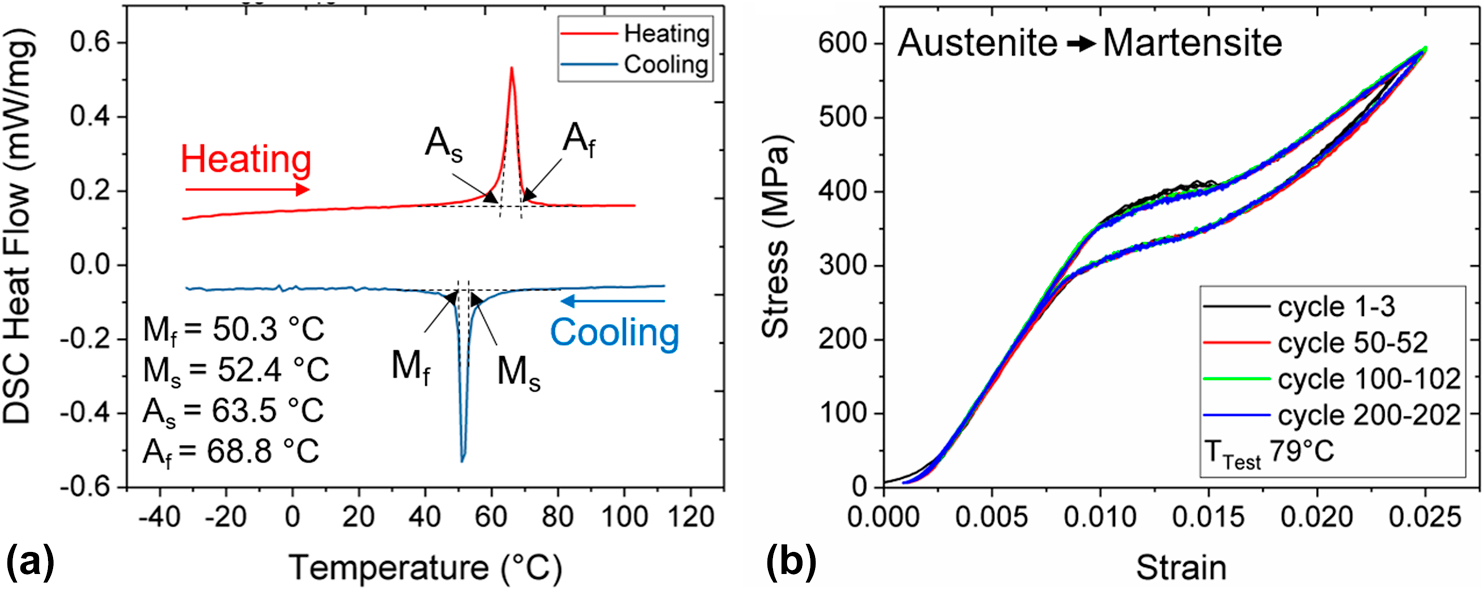
Figure 3(a) shows a differential scanning calorimetry (DSC Netzsch 204F1Phoenix) measurement of a 20-μm thick TiNiCu film after annealing at 700 °C for 15 min. The austenite and martensite transformation temperatures (i.e., A s = 63.5 °C, A f = 68.8 °C, M s = 52.4 °C, and M f = 50.3 °C) occur at a moderate temperature suitable for ME sensor operations. These transformation temperature measurements are in good agreement with temperature-dependent XRD measurements on the fabricated composites, discussed in the Supplementary material III. A tensile testing (Zwick Roell Z.05) plot of TiNiCu after annealing is shown in Fig. 3(b). When TiNiCu is pulled to an elongation of 2.5% (strain = 0.0025) for 200 cycles, there was very little observed structural and functional fatigue demonstrated in the SMA's hysteresis loop. This is also in agreement with the literature where previously TiNiCu thin films of similar composition were found to be ultralow fatigue materials, reversibly undergoing the phase transformation 107 times with minimal functional fatigue demonstrated in the hysteresis loop [Reference Chluba, Ge, de Miranda, Strobel, Kienle, Quandt and Wuttig16].
Shape memory alloy characterization of freestanding TiNiCu film annealed to 700 °C for 15 min. (a) Differential scanning calorimetry curves show the austenite and martensite transformation temperatures of the sample. (b) Exemplary tensile testing plot of a TiNiCu dogbone reversibly stretching to a strain of 0.025, 200 times with no observable fatigue.

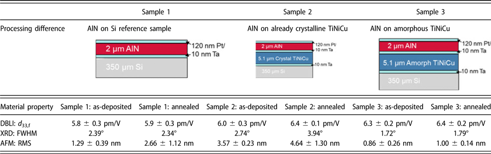
Piezoelectric characterization of (002) AlN
c-axis (002) AlN polycrystalline thin-film growth is known to be highly dependent on the underlying substrate surface roughness [Reference Yarar, Hrkac, Zamponi, Piorra, Kienle and Quandt28, Reference Pawar, Singh, Sharma, Pandey, Dutta and Kaur33]. Variations in the structural and piezoelectric properties are evaluated for sputtered polycrystalline AlN onto (111) Pt seed layers on three substrates: Si (Sample 1), already crystalline TiNiCu on Si (Sample 2), and amorphous TiNiCu on Si (Sample 3). Sample 3 must be annealed after AlN deposition to crystallize the underlying TiNiCu film (Sample 3: annealed). To provide a complete comparison, Sample 1 and Sample 2 were also characterized after annealing the composites (i.e., Sample 1: annealed and Sample 2: annealed).
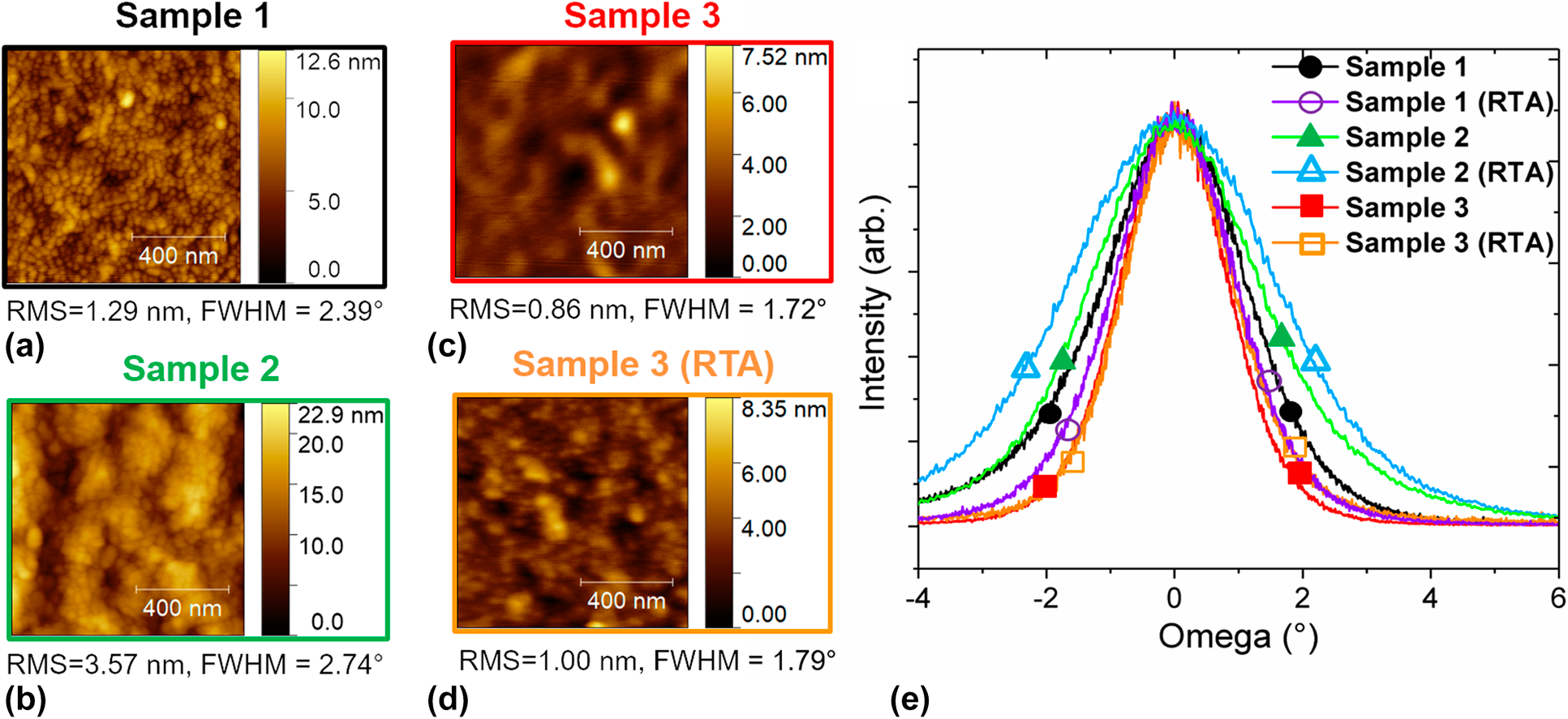
Nanoscale imaging of the surface topography (root mean squared—RMS) with atomic force microscopy (AFM) in tapping mode was conducted on at least three different locations on all samples. These surface roughness measurements were then correlated with the structural crystallinity of AlN, revealed by the full width at half maximum (FWHM) XRD rocking curve (ω scans) about the (002) AlN peak (2θ = ∼36.7°). A narrow FWHM typically indicates a highly textured (002) AlN with columnar c-axis growth, thus better quality AlN film and higher d 33,f [Reference Iqbal and Mohd-Yasin34]. Figure 4(a) shows a 1-μm × 1-μm AFM image of Sample 1: as-deposited (reference sample), (002) AlN on smooth Si substrate with a low surface roughness of RMS = 1.29 nm ± 0.39 nm and FWHM = 2.39°. Fig. 4(b) shows AlN deposited onto already crystalline TiNiCu (Sample 2: as-deposited) has a larger surface roughness RMS = 3.57 nm ± 0.23 nm and larger FWHM = 2.74°. As shown in Fig. 4(c), the lowest surface roughness is obtained when AlN is deposited onto an amorphous TiNiCu film of RMS = 0.86 nm ± 0.26 nm with the narrowest FWHM = 1.72° (Sample 3: as deposited). The AFM map in Fig. 4(d) shows that upon annealing the AlN/amorphous TiNiCu/Si composite to 700 °C (Sample 3: annealed), the surface roughness slightly increased from 0.86 nm ± 0.26 to 1.00 nm ± 0.14 nm, which only corresponded to a slight increase in the FWHM from 1.72° to 1.79°. The rocking curve measurements used to calculate the FWHM value for all samples are shown in Fig. 4(e).
Structural characterization of (002) AlN grown onto various substrate types. AFM surface roughness measurements. (a) Sample 1: (100) Si (reference sample) (black), (b) Sample 2: already crystalline TiNiCu (green), (c) Sample 3: amorphous TiNiCu (red), and (d) Sample 3 after annealing: amorphous TiNiCu then crystallized (orange). (e) X-ray diffraction rocking curve (ω scans) of the (002) AlN peak (2θ = ∼36.7°) and FWHM for each sample shown in (a)–(d).
The effective longitudinal piezoelectric coefficient (d 33,f ± standard deviation) was determined through standard double beam laser interferometry (aixACCT Systems, aixDBLI) measurements [Reference Prume, Tiedke and Schmitz-Kempen35, Reference Burianova, Bowen, Prokopova and Sulc36]. DBLI polarization and displacement curves were compared for Samples 1–2 in the as-deposited state and Sample 3 after annealing. Polarization measurements in Fig. 5(a) demonstrate Sample 1 has an average d 33,f coefficient of 5.8 pm/V ± 0.3 pm/V, on par with the state-of-the-art values reported for low-temperature sputtered AlN [Reference Yarar, Hrkac, Zamponi, Piorra, Kienle and Quandt28]. Sample 1 also displays a typical linear polarization behavior with similar characteristics to AlN sputtered onto other electrodes (Ti, Pt, and Al) on Si substrates [Reference Pawar, Singh, Sharma, Pandey, Dutta and Kaur33]. The d 33,f value is found to slightly improve when AlN is sputtered onto (111) Pt on both amorphous and crystalline TiNiCu thin films on Si substrates. Despite the large surface roughness in Sample 2, the typical linear polarization behavior of AlN was observed in Fig. 5(b), with a high longitudinal piezoelectric coefficient d 33,f = 6.0 pm/V ± 0.3 pm/V. A linear polarization loop and an even larger d 33,f coefficient was obtained when AlN was deposited onto amorphous TiNICu for Sample 3 as-deposited (d 33,f = 6.3 pm/V ± 0.2 pm/V). However, Fig. 5(c) shows the annealing step results in an open polarization loop for Sample 3-annealed. This indicates the AlN layer in Sample 3-annealed has a higher conductivity and higher resistive losses than the other samples. A summary of all DBLI measurements are given in Table SII (Supplementary material IV). The d 33,f and polarization curves of all samples in the as-deposited state and after annealing state are shown in Fig. S4 (Supplementary material IV). These results prompted investigation of the interfaces to correlate microstructure changes to the electrical and structural properties of sputtered AlN. Table II shows a summary of all investigated piezoelectric properties of each sample in both the as-deposited state, and after annealing at 700 °C for 15 min.
Polarization and displacement curves obtained from DBLI measurements with an applied electric field between ± 500 kV/cm. (a) Sample 1: as-deposited, (b) Sample 2: as-deposited, and (c) Sample 3: annealed.

Summary of investigated (002) AlN piezoelectric properties of samples as-deposited and after annealing at 700 °C for 15 min.
Microstructural characterization of AlN on crystallized and amorphous TiNiCu
The chemical integrity, surface morphology, and interface study of the composites fabricated by the two different approaches are analyzed with STEM Z-contrast images and energy-dispersive X-ray spectroscopy (EDS). A cross-section image of Sample 2 is shown in Fig. 6(a). The crystalline texture of the AlN film was analyzed by electron diffraction (ED) experiments which show a 5° out-of-plane tilt for the c-axis columnar texture of the (002) AlN film depicted in Fig. 6(b). Annealing the TiNiCu before AlN deposition results in a polycrystalline structure with grains sizes of TiNiCu in the range of 100–400 nm and of different stoichiometry apparent from the brighter and darker Z-contrast. To link the observed differences in Z-contrast and morphology in the TiNiCu film to the chemical composition, Fig. 6(c) shows the EDS profiles along the interface region (yellow arrow) and quantified according to the stoichiometry at each measured data point.
(a) STEM image of the cross-section through Sample 2. The yellow arrow labels the position of the EDS profile. (b) ED pattern of the AlN film demonstrating partial out-of-plane tilt of 5° columnar grains. (c) EDS profile showing the quantitative atomic distribution across the interface between AlN and TiNiCu. (d) STEM image of the cross-section of Sample 3 after annealing. (e) ED pattern of the AlN film. (f) EDS profile showing the quantitative atomic distribution across the interface between AlN and TiNiCu.

The dashed black lines differentiate between grains of different Z-contrast and grain morphology, especially at the 140-nm-thick interface region. Following the element profiles from left to right, the high Z-contrast grains of TiNiCu yields the targeted composition of ∼Ti50Ni35Cu15. However, on entering the first low Z-contrast grain, the amounts of Ti and Cu increase, whereas Ni decreases, yielding an average composition of ∼Ti66Ni14Cu20. Close to the interface, the Ni content increases, whereas Cu decreases, giving a different average composition of ∼Ti65Ni31Cu4, followed by separate and distinct layers of Ta, Pt, and AlN. A detailed characterization of further common precipitates present in TiNiCu films such as Ti2Cu was not performed in this study. However, for an in-depth discussion of the Ti2Cu role the reader is referred to Dankwort et al. [Reference Dankwort, Strobel, Chluba, Ge, Duppel, Wuttig, Quandt and Kienle37]. The heterogeneous variation in TiNiCu grain stoichiometry would be problematic for reliable ME sensor operation because the stoichiometry is known to strongly influence the formation enthalpies leading to degeneracy of the transformation temperatures within the film; hence, only partial transformations would be observed on heating to a specific temperature [Reference Gu, Bumke, Chluba, Quandt and James20, Reference Frenzel, Wieczorek, Opahle, Maaß, Drautz and Eggeler38].
In comparison, the cross-section and ED pattern of the AlN film of Sample 3 are presented in Figs. 6(d) and 6(e) together with the EDS profiles given in Fig. 6(f). The most apparent difference between the two composites is the formation of a ∼420-nm-wide diffusion region expanded over the Ti-enriched and Cu-poor TiNiCu grains at the interface to the bottom Ta/Pt electrode by interdiffusion upon RTA. Further discussion about the envisioned diffusion process can be found in the Supplementary material V. This Ti-enriched and Cu-poor interface grain structure (∼340 nm) is evidenced also at the Si substrate/Ta interface. The ED pattern on the AlN film provides evidence of an excellent c-axis texture without any misalignment in the analyzed area of the film.
Concerning the stoichiometry of the SMA film, smaller variations in the Z-contrast images are observed, and an average composition of ∼Ti50Ni33Cu17 was measured by EDS. However, close to the diffusion region, the EDS profiles indicate larger stoichiometric deviance of the TiNiCu composition than the average composition. Here, it is assumed that Ti diffused into the Ta/Pt layers, breaking up the electrode structure. As a result, Ni (∼40 at.%) accumulated in the intermediate interface region with respect to the average film stoichiometry. The transformation from the martensite phase (room temperature) into the austenite (120 °C) phase was probed by in situ heating experiments collecting diffraction information at room and high temperature for both samples. The results are discussed in Fig. S5 (Supplementary material V).
Conclusions
High-quality c-axis oriented (002) AlN films were obtained on ultralow fatigue TiNiCu shape memory alloy thin films on Si substrates. Analytical calculations demonstrate that a wide range of tunability is possible by incorporating ME composites onto thin-film SMA. Variations in the piezoelectric performance of AlN are found to be strongly correlated to the underlying film's surface roughness, grain size, and thickness. While the best crystalline (002) AlN films were obtained on amorphous TiNiCu (Sample 3: As-deposited, d 33,f = 6.3 pm/V ± 0.2 pm/V), annealing the composite to 700 °C to crystallize the SMA-promoted interdiffusion of Ti into the Ta adhesion layer and Pt electrode layer. There was little observed change in the large longitudinal piezoelectric coefficient from the annealing step (Sample 3: annealed, d 33,f = 6.4 pm/V ± 0.2 pm/V); however, an open polarization loop was observed, which indicates a high leakage current in the AlN film. In the case where AlN is sputtered onto already crystalline TiNiCu, a large piezoelectric coefficient is obtained (Sample 2: as deposited, d 33,f = 6.0 pm/V ± 0.3 pm/V), despite the large surface roughness of crystalline TiNiCu causing a 5° misalignment in the c-axis direction. Furthermore, the expected linear polarization [Reference Pawar, Singh, Sharma, Pandey, Dutta and Kaur33] of AlN is obtained for this sample; therefore, this method is found to be the most promising fabrication route for tunable ME composite applications.
Polycrystalline sputtered AlN will display its best mechanical and electrical performance when deposited onto a substrate with low surface roughness [Reference Yarar, Hrkac, Zamponi, Piorra, Kienle and Quandt28, Reference Pawar, Singh, Sharma, Pandey, Dutta and Kaur33]. Because the structural quality of TiNiCu is dependent on the annealing conditions of the composite, future studies should consider significantly lower annealing temperatures (∼500 °C) because it was reported to reduce the small grain size and surface roughness for TiNiCu [Reference Fu, Du, Zhang and Gu22]. Another possible solution to reduce the surface roughness of the SMA before AlN deposition is through a chemical-mechanical polish or an electropolishing treatment [Reference Pohl, Heßing and Frenzel39]. Alternatively, these issues could entirely be circumvented if one were to deposit and crystallize the SMA on one side of the silicon wafer followed by the structuring of an AlN/FeCoSiB inverse bilayer sensor onto the other side of the wafer [Reference Yarar, Salzer, Hrkac, Piorra, Höft, Knöchel, Kienle and Quandt30].
Methods and materials
Piezoelectric characterization
DBLI measurements were performed on all samples in a parallel plate capacitor geometry on an aixACCT Systems aixDBLI tool. Polarization and displacement curves were taken at a minimum of three spots on each samples to generate an average d33,f at each applied voltage (i.e., 10 V, 20 V, 50 V, and 100 V). The slope of the displacement curves at each applied voltage is used to obtain d 33,f.
Structural characterization
AFM measurements were obtained on an AIST-NP SPM 1000 instrument in noncontact tapping mode were conducted using a 160-µm-long arrowhead tip [NanoWorld Arrow NC]. XRD (SmartLab 9 kW, Rigaku) ω rocking curve measurements were performed in a ω range ±10° around the (002) AlN peak (2θ = ∼36°) with a step size of 0.02° and a scan speed of 1° per min.
Microstructural characterization
The samples were investigated using transmission electron microscopy operated in scanning (STEM) mode on a Tecnai F30 G2 Twin instrument equipped with a Si/Li-drift detector (EDAX system) for energy-dispersive X-ray spectroscopy (EDS) analysis. The samples have been prepared to electron transparency by the focused ion beam (FIB) method using Ga-ions and Pt protection layers during the thinning procedure.
Supplementary material
To view supplementary material for this article, please visit https://doi.org/10.1557/jmr.2020.106.
Acknowledgments
This work was supported by the German Research Foundation (Deutsche Forschungsgemeinschaft, DFG) through the Collaborative Research Centre CRC 1261 Magnetoelectric Sensors: From Composite Materials to Biomagnetic Diagnostics. This material is based on the work supported by the National Science Foundation Graduate Research Fellowship under Grant No. DGE 1840340. The authors thank Prof. Dr. Klaus Rätzke for his assistance in discussing the diffusion processes.


 Open access