


Introduction
In recent years, the need for integrated sensors has increased. A reason is the novel trend of Internet of Things (IoT), which allows completely new applications and opportunities in the industrial and in the upcoming biomedical area [Reference Guarin, Hofmann, Nehring, Weigel, Fischer and Kissinger1]. In connection with IoT, wearables with biomedical focus are a new application, which needs integrated sensors. Wearables can be used to detect many different vital parameters. This allows a very precise image of the current state of health of the user. With the identification of the composition of biological tissues inside the human body, a more accurate analysis of the user’s condition is possible [Reference Guarin, Hofmann, Nehring, Weigel, Fischer and Kissinger1]. For the future, a promising approach are non-invasive microwave biosensors, which use electromagnetic waves for detection of the vital parameters. This approach is preferable for wearables, because of its non-invasive measurement principle and the compact size. Microwave sensors are well suited not only for biological application but also for the characterization in industrial surroundings, where they open completely new opportunities. For example, microwave sensors enable robots to perceive their near surrounding in this way that they can distinguish biological materials from other materials. This is important e.g. for the interaction with humans. One often used class of microwave sensors are broadband sensors, like open waveguide sensors or the coaxial probe [Reference Guarin, Hofmann, Nehring, Weigel, Fischer and Kissinger1]. They exhibit a bandwidth over a frequency range of several GHz. A possible readout device for this kind of sensors are monolithically integrated vector network analyzers (VNA) [Reference Nasr, Nehring, Aufinger, Fischer, Weigel and Kissinger2]. For the translation of such broadband signals to a much lower fixed intermediate frequency, a multi-octave receiver front-end is necessary. This paper presents a receiver with a frequency range of 1−32 GHz. Such a high input bandwidth demands several bandwidth-extensions for reaching both, a well-matched input of the receiver over the whole bandwidth, as well as a high and flat gain-function. Both are necessary for the quality of the measurement performance of the integrated VNA, as well as for an accurate calibration. Furthermore, an enhanced gain control functionality is essential to handle the very different power levels of the measured input signal, but without the loss of input matching for decreased gain levels, as it is the case of standard gain control circuits.
SiGe technology
The shown receiver components are realized in the B7HF200 SiGe technology, a 0.35 μm bipolar technology from Infineon Technologies AG [Reference Böck, Schäfer, Aufinger, Stengl, Boguth, Schreiter, Rest, Knapp, Wurzer, Perndl, Böttner and Meister3]. For active circuits, three different types of NPN transistor are available: the ultra high speed (UHS), the high speed (HS), and the high voltage (HV). In addition, high-performance varactors are available for active circuits [Reference Vytla, Meister, Aufinger, Lukashevich, Boguth, Knapp, Böck, Schäfer and Lachner4]. Furthermore, three types of resistors can be used. Besides two poly resistors with sheet resistances of 1000 Ω/sq and 150 Ω/sq, a TaN thin film resistor can be used, which has a sheet resistance of 20 Ω/sq. The B7HF200 technology offers four copper metalization layers with thicknesses of 600, 600, 1200, and 2500 nm, respectively [Reference Böck, Schäfer, Aufinger, Stengl, Boguth, Schreiter, Rest, Knapp, Wurzer, Perndl, Böttner and Meister3]. The upper layer with 2500 nm is predestined for passive structures, like spiral inductors, which benefit from the low resistivity due to the high cross-section of the upper metal layer. This allows inductances with a high-quality factor. Also, a metal-insulator-metal (MIM)-capacitor is included in the four-layer metal stack.
System overview
3-Channel front-end
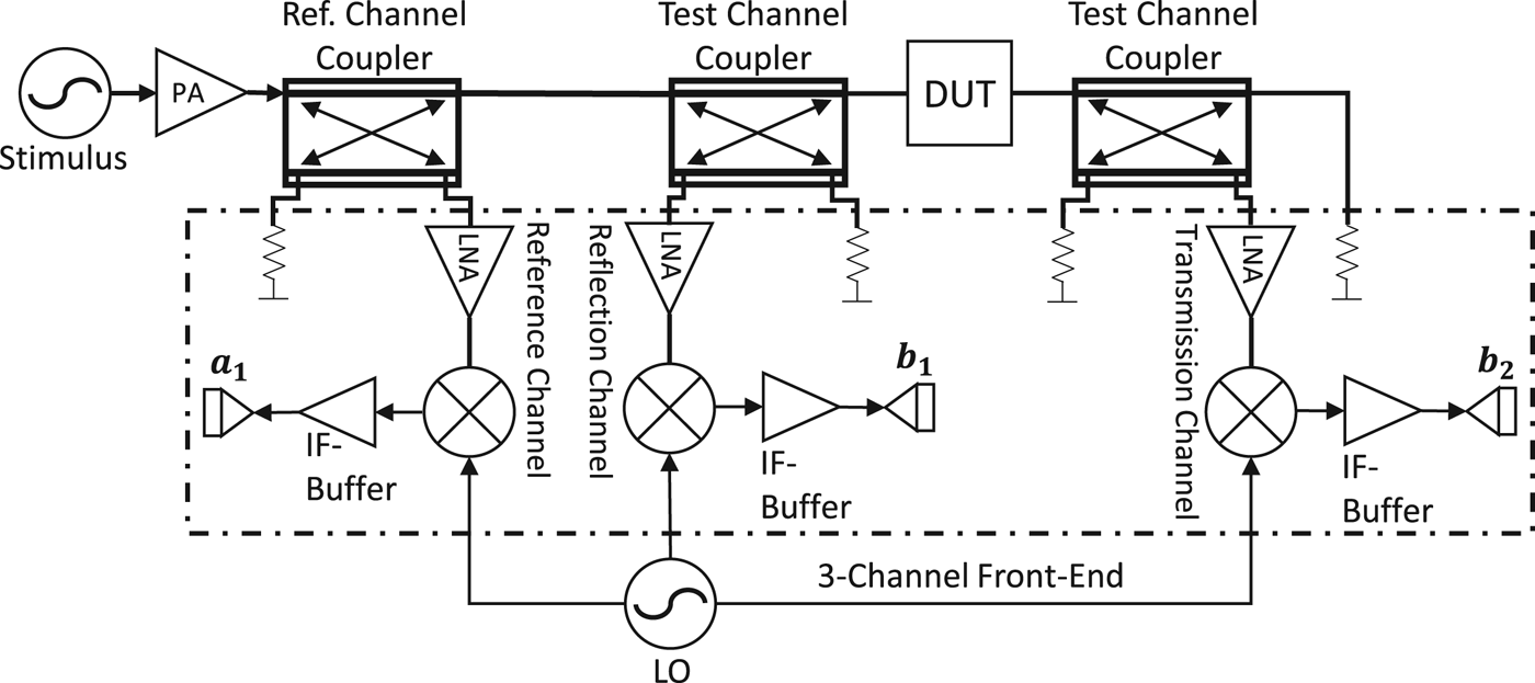
For the use in a monolithic integrated VNA, which can determine the reflection- and the transmission-coefficients of a DUT, a front-end with minimum three or more receiver chains is necessary. A simplified representation of a 2-Port VNA is shown in Fig. 1, which is based on [Reference Nasr, Nehring, Aufinger, Fischer, Weigel and Kissinger2, Reference Dunsmore5]. For the measuring of complex S-Parameters, besides the determination of the amplitude, the phase has to be detected. Therefore, a comparison between the phase of the stimulus and the phase of the reflected or transmitted signal, respectively, has to be done, in addition to the comparison of the magnitudes. This requires an additional receiver, which measures the stimulus signal. This additional receiver chain is typically named as reference channel (see Fig. 1) and allows a vectorial measurement of the S-Parameters. It is important to use a coherent receiver architecture, to get both, the magnitude and the phase of the received signal portion [Reference Nasr, Nehring, Aufinger, Fischer, Weigel and Kissinger2]. Since the quality of the S-Parameter measurements depends directly on the quantity of the signal portion of the respective test channel and of the reference signal, it is obvious that any superposition through crosstalk or feedthrough has to be avoided. Therefore, the isolation between the receiver chains has to be as high as possible, as well as the isolation inside a receiver chain [Reference Dunsmore5].
Simplified representation of a 2-port VNA with 3 receiver channels based on [Reference Nasr, Nehring, Aufinger, Fischer, Weigel and Kissinger2, Reference Dunsmore5].
Multi-octave receiver chain
The realized receiver chain consists of an ultra-broadband low noise amplifier (LNA), followed by a broadband active mixer with an integrated IF buffer, which is shown in Fig. 2. The proposed receiver is based on a heterodyne architecture with an IF frequency of 1 GHz. In the context of biological test material, the variable gain control circuit (VGC) of the LNA is realized with an additional shunt feedback in the VGC circuit, to achieve an adequate input matching for all adjusted gain levels. This is a special added extension for the use case of the receiver in a VNA. The advantage of this topology is that low gain levels do not result in input mismatch of the receiver. This prevents multiple reflections between the test port of the VNA and a bad matched DUT, like it is often the case for biological materials. The LNA exhibits a second variable-gain functionality on its output, to improve the tuning precision and the isolation of the receiver chain if it is turned off. Furthermore, the second gain control function is necessary, to enable a precise handling of very different input power levels, which are typical for biomedical applications. This allows a very accurate regulation of output power level for the next receiver stages.
System overview of the presented broadband receiver. It consists of a LNA and an active mixer with an integrated IF output buffer.

Circuit design
LNA
For achieving the enormous bandwidth from 1 to 32 GHz, several techniques must be used to get a high and flat gain over this frequency range, as well as a good input matching and a low noise figure at the same time. If only one bandwidth extension method is used, especially the 3 dB-criterion of the gain would be exceeded. A combination of several methods enables a gain characteristic of the LNA, which meets the 3 dB-criterion over a very large frequency range. After the description of the basic topology, the used techniques are presented in detail, namely the shunt feedback, the shunt peaking and a special tuned emitter follower stage (EF).
Basic topology
The basic topology of the LNA is the well-known cascode (CC). For broadband amplifiers in general, it is one of the favorite basic topologies, because of its reduced Miller effect. The Miller effect is mainly caused through the parasitic Miller-Capacitance C m between the collector and the base node of a common emitter stage (CE). The reduction of this capacitance is achieved through the low input impedance of a common base stage (CB), which is stacked onto the collector node of the CE. Furthermore, this reduces the time constant τ ≈ R L · C m and enhances, in the same way, the bandwidth of the LNA. A drawback of the topology-based bandwidth enhancement is the slightly higher noise figure. The reason for that is the additional noise contribution of the CB stage. Additionally, the isolation of the LNA benefits also from the stacked CB transistor, which is important for a VNA. The gain of a basic CC can be described (based on [Reference Razavi6, Reference Gray, Hurst, Lewis and Meyer7]) in a good approximation with the following expression:
 $$ A_{V}(s)=-{g}_{m} \cdot (\underline{{Z}}_{out,CC}(s) \vert \vert \underline{{Z}}_{L}(s)). $$
In equation (1), g m is the transconductance, Zout,CC(s) describes the output impedance of the CC and ZL(s) stands for the load impedance, which is seen by the CC. Equation (1) shows that the gain of the basic CC depends directly from the load impedance ZL(s), and indirectly from the load current, which affects the transconductance g m.
Techniques for bandwidth extension
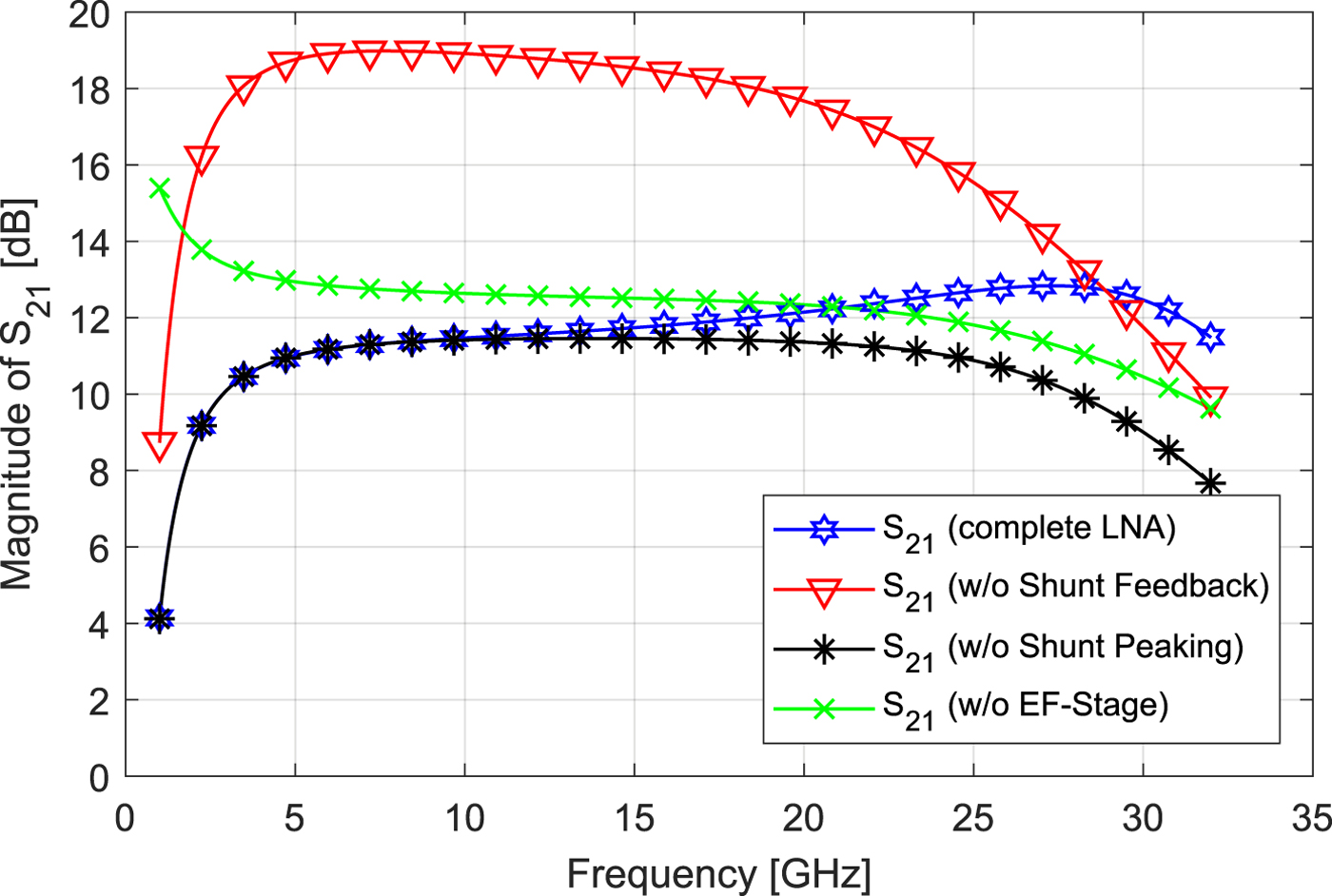
As mentioned above, a combination of various techniques is necessary to reach a bandwidth over several octaves. The first technique for bandwidth extension is a shunt feedback (FB1) from the CC output node to the base of the common emitter circuit of the CC, which can be seen in Fig. 3. The shunt feedback consists of a series connection of a TaN resistor R f and a MIM capacitor C f. A CC stage in its basic configuration exhibits a high gain at low frequencies. To flatten the gain at low frequencies, the proposed shunt feedback (FB1) can be used, because it reduces the gain peak of the basic CC at low frequencies and pushes simultaneously the 3 dB cut-off frequency towards a higher range. This behavior can be observed by comparing the simulation results of Fig. 4. Gain and bandwidth are coupled by the gain-bandwidth product (GBW) [Reference Gray, Hurst, Lewis and Meyer7]. Therefore, the gain reduction results in a higher bandwidth.
To improve the frequency bandwidth further, shunt peaking is implemented in the LNA. In case of shunt peaking, an additional inductance L C is implemented in series with the collector branch of the CC, as can be seen in Fig. 3. This inductance is realized as a spiral inductor on the top metal layer of the used B7HF200 technology. To get an accurate simulation model for the shunt peaking inductance, the spiral inductor was simulated with the 2.5-D simulator from Sonnet Software, Inc. For higher frequencies, the impedance of the inductor L C increases and compensates the reduction of the output impedance Zout,CC(s), which is caused by the equivalent capacitance C eq on the output of the CC. The equivalent capacitance C eq summarizes all capacitances on the CC’s output. This results in an increased gain over a wider frequency range, compared to the basic CC circuit. With the right choice of the value of the inductor L C, the impedance of L C helps to reach a flat gain variation over the extended frequency range. From the time domain point of view, a higher bandwidth can be achieved by reducing the time constant τ of the CC output [Reference Lee8]. In this case, especially the rise time  ${t_{C_{eq}}}$ of the parasitic capacitor C eq is important [Reference Lee8]. Through the delayed current flow caused by the inductor L C, the current-need of the parasitic capacitance can be better fulfilled [Reference Lee8]. Hereby, the time constant on the output of the CC can be reduced and the overall bandwidth can be extended. For simplification, the following examinations for shunt peaking is done on a single-ended CC. The load impedance ZL consists of a series connection of the load resistance R L and the added inductance L C, which are in parallel to the parasitic capacitances of the CC output. All capacitances are summarized in C eq. The impedance Z L of the resulting equivalent circuit can be expressed according to [Reference Lee8] as follows:
 $$ \underline{Z}_{L}(s)=(sL_C + R_L) \parallel \displaystyle{1 \over sC_{eq}}, $$
Schematic of the presented LNA with the variable gain control circuit for input matching and flat gain for all gain control levels. It includes all bandwidth extension methods. Biasing is not shown here.

Simulated influences of the different bandwidth extension methods to the gain function of the LNA. To demonstrate the impact of each method, the respective circuit part was deactivated during the simulation.
which can be rearranged in
 $$ \underline{{Z}}_{L}(s)={\displaystyle{R_L [1+s({L_C}/{R_L})]} \over{1+sR_L C_{eq}+s^{2}L_C C_{eq}}}. $$
If the magnitude of (3) is formed, the effect of the additional inductance L C can be further investigated:
 $$ \left\vert Z_L(\,j\omega) \right\vert = {R_L \sqrt{\displaystyle{(\omega {L_C}/{R_L})^2 + 1} \over{(1-\omega^2 L_C C_{eq})^2 + (\omega R_L C_{eq})^2}}}.$$
By a closer view on (4), two additional terms are perceptible related to the basic function of a RC-circuit at the output. In detail, these are the term (ωL C/R L)2 in the numerator and the term (1 − ω 2L CC eq)2 in the dominator. Both terms yield to a higher bandwidth. The first one increases the impedance |Z L(jω)| for rising frequencies and the second one increases the impedance |Z L(jω)| as well for frequencies below the resonance frequency of the LC-circuit [Reference Lee8]. Additionally, the influence of shunt peaking to the gain function of the LNA is shown by simulation. By comparing the corresponding simulated curves in Fig. 4, the bandwidth extension through shunt peaking can be observed.
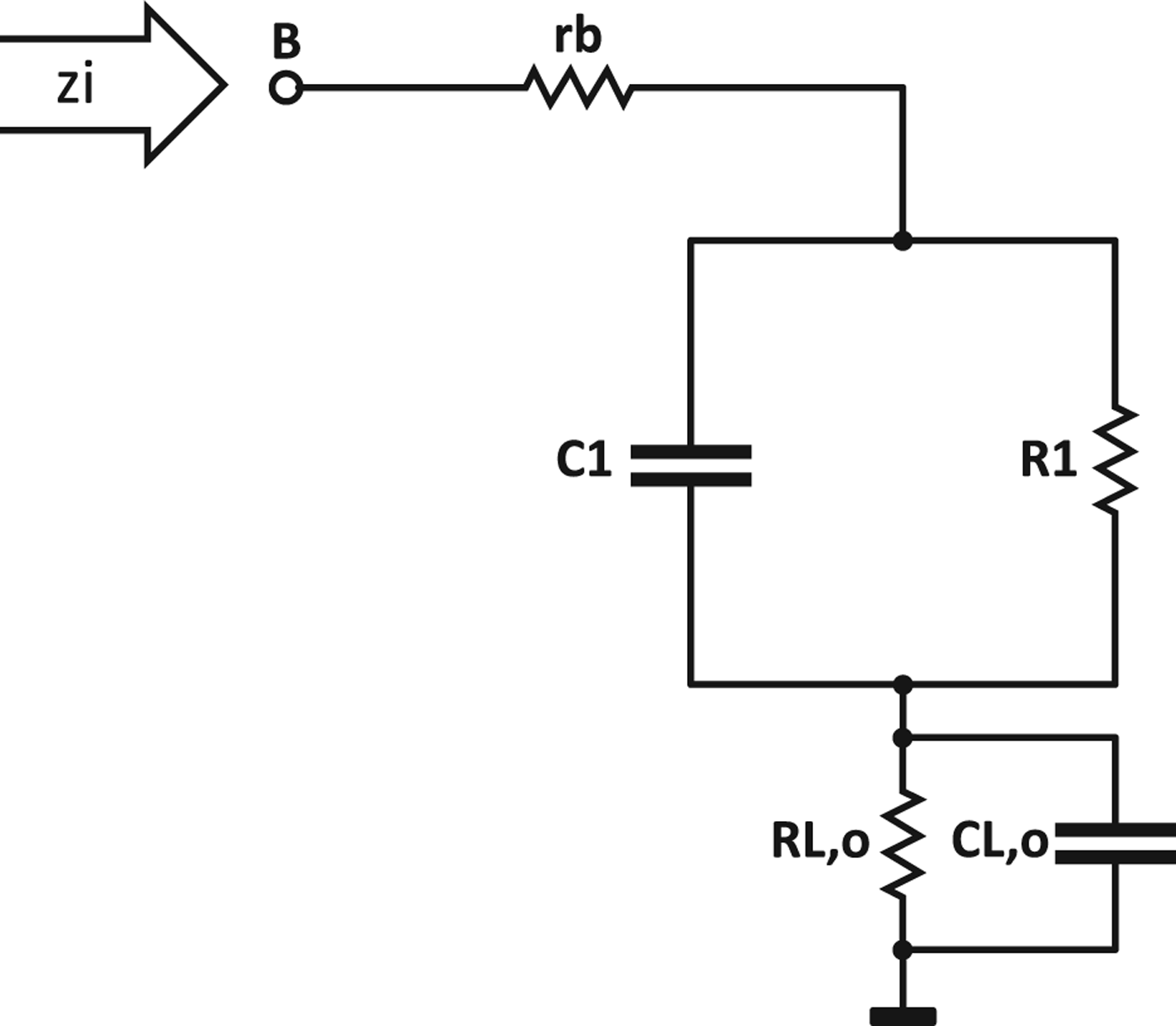
With EF, the bandwidth can be further increased, as shown in Fig. 4. For this, the EF has to be loaded capacitively and moreover, specific biasing conditions must be met. The goal is a RLC series resonant behavior of the EF [Reference Trotta, Knapp, Aufinger, Meister, Böck, Dehlink, Simbürger and Scholtz9]. This leads to a gain peak at high frequencies. In combination with the gain distribution of the above described enhanced CC, the overall gain bandwidth is considerably increased, as can be seen in Fig. 4. Different to [Reference Trotta, Knapp, Aufinger, Meister, Böck, Dehlink, Simbürger and Scholtz9], the EF is placed at the output rather than at the input. This allows a much better input matching, which is important for a VNA. The EF can be seen in Fig. 3 with a current mirror biasing, which realizes the second VGC functionality (VGC_EF). To understand why the EF exhibits gain under specific conditions, it is necessary to analyze the dominant parts of the input and output impedance and the resulting behavior of the transfer function. The input impedance z i (see Fig. 5) of a single-ended emitter follower consists in a good approximation of a series connection with the series base resistance r b, a load resistor R L,o and a parallel connection, which can be represented by an equivalent resistor R 1 and a capacitor C 1 [Reference Gray, Hurst, Lewis and Meyer7]. The equivalent circuit is shown in Fig. 5. According to [Reference Gray, Hurst, Lewis and Meyer7], the resulting expression for the equivalent input impedance z i is
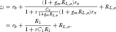 $$\eqalign{z_i &= r_b + {\displaystyle{{(1 + g_m R_{L,o})r_\pi } \over {1 + s {C_\pi \over 1 + g_mR_{L,o}} (1 + g_mR_{L,o})r_\pi }} + R_{L,o}} \cr & = r_b + {\displaystyle{{R_1} \over {1 + sC_1R_1}}} + R_{L,o}.} $$
In equation (5), r π represents the small signal input resistance, whereas C π is the parasitic capacitance parallel to r π. The small signal resistor r b stands for the series resistance of the base node.
Equivalent circuit of the input impedance z i of an EF with capacitively loaded output C L,o [Reference Gray, Hurst, Lewis and Meyer7].
For the equivalent elements R 1 and C 1 the following expressions can be determined [Reference Gray, Hurst, Lewis and Meyer7]:
 $$ R_1=(1+g_mR_{L,o})r_{\pi}, $$
and
 $$ C_1={\displaystyle{C_{\pi}} \over{1+g_mR_{L,o}}}. $$
If the output of the EF is capacitively loaded, which is represented in Fig. 5 by the capacitance C L,o, the input impedance of the EF exhibits also a capacitive behavior, because the capacitor C L,o on the output is in parallel to the load resistor R L,o, which is a series component of the input impedance. If the condition 1/g m < (R s + r b) is met through a high biasing current and a large impedance of the source R S, which is presented here through the output of the CC, the EF acts for high frequencies on its output like an inductor [Reference Razavi6, Reference Gray, Hurst, Lewis and Meyer7, Reference Trotta, Knapp, Aufinger, Meister, Böck, Dehlink, Simbürger and Scholtz9]. As a result, the EF exhibits the same behavior as a RLC circuit. For simplification and focusing on the effect itself, a single-ended version of the EF is assumed in the following mathematical expressions. As shown in [Reference Trotta, Knapp, Aufinger, Meister, Böck, Dehlink, Simbürger and Scholtz9], the function of the gain can be approximated with the following expression for a single-ended EF:
 $$ \eqalign{& A(\,j\omega) \approx \displaystyle{1 \over 1\!+\!j\omega\left[r_b C_{\mu} \left({1 \over g_m} \!+\! {r_b \over \beta} \right) C_{L,o}\! +\! {r_b C_{L,o\!} \over \omega_T R_{eq,o\!}} \right]\! -\! \omega^2 {r_b C_{L,o} \over \omega_T}}}.$$
In equation (8), R eq,o stands for the parallel connection of the output resistance r o of the transistor and the resistive part of the load R L,o. C μ is the parasitic capacitance between base and collector. From equation (8), the resonance frequency ω r can be determined to
 $$ \omega_r = \sqrt{{\displaystyle{\omega_T} \over{r_b C_{L,o}}}}. $$
As a result, equation (9) shows that the frequency with the maximum gain peak is anti-proportional to the load capacitance C L,o and depends on the collector current density j C, which influences the transit frequency ω T of the emitter follower. In the shown LNA, the EF shifts the gain peak up to approximately 28 GHz, as can be seen in Fig. 4.
Broadband input matching
Just as with the gain function, for a wideband input matching over several decades, a combination of different matching mechanisms is necessary. For the presented LNA, two different methods are combined as can be seen in Fig. 3. To achieve an input matching for the desired bandwidth from 1 to 32 GHz, a π-network is realized at the input of each branch of the quasi-differential CC and additionally, a second method in form of a shunt feedback (FB1) is implemented, which can be seen in Fig. 3. The second method is also used for bandwidth extension of the gain function, as described before.
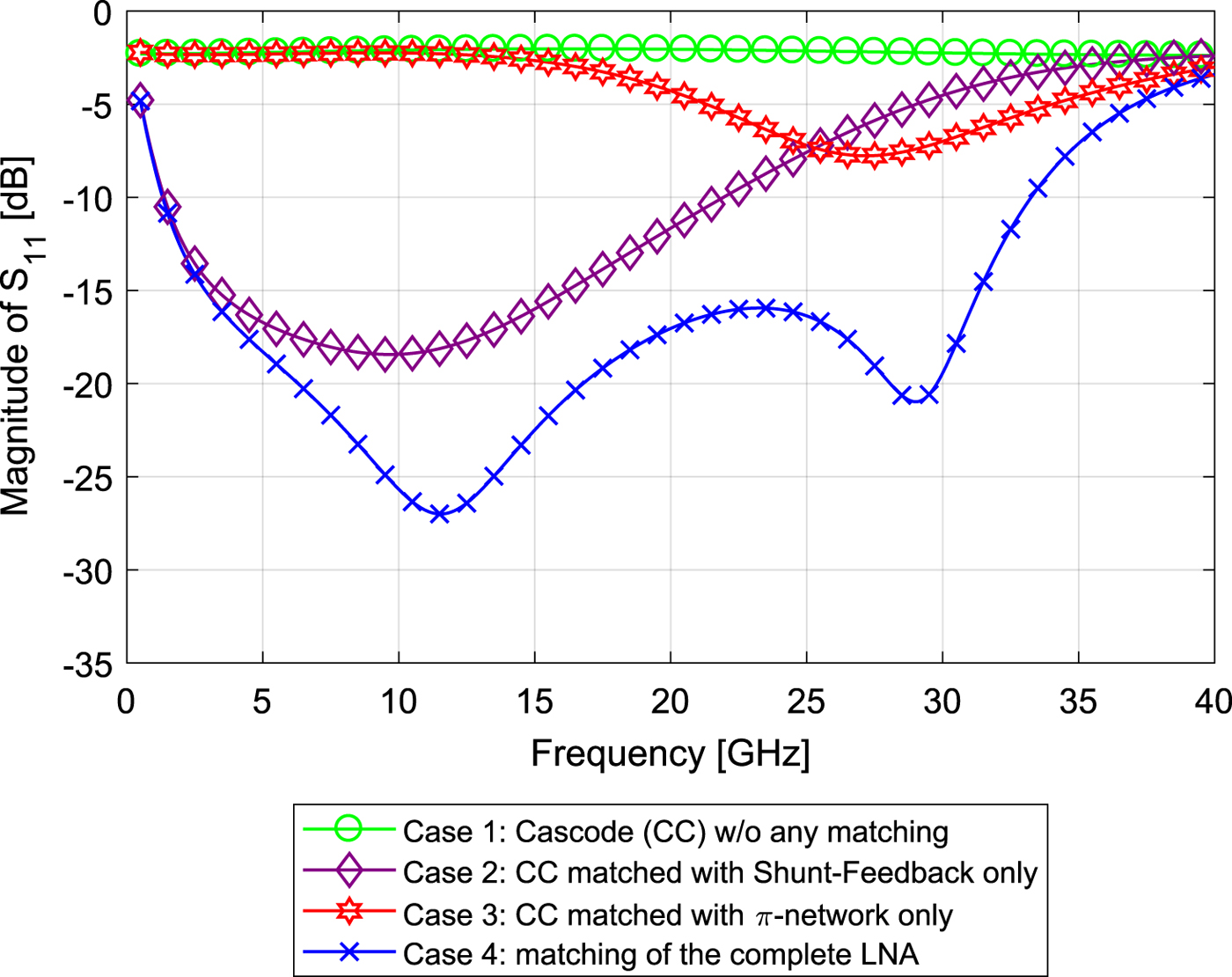
The major impact on the input matching function comes from the feedback branch (FB1), which is implemented between the output node and the input node of the CC on each half-circuit of the LNA. In Fig. 6, the effect of the shunt feedback (FB1) can be seen by the comparison of the curve (Case 2) with the matching function of the completed LNA (Case 4) with all matching methods included. By a qualitative comparison of both curves, it becomes obvious that for the frequency range below approximately 23 GHz the matching is mainly determined by the shunt feedback (FB1). The CC itself has an input impedance Zin, which exhibits a strong influence from its base-emitter capacitance C π. In Fig. 7, this behavior is shown in Case 1 (see also Fig. 6, Case 1), where the CC is simulated without any matching. The shunt feedback leads to a reduction of the imaginary part of the input impedance Zin for low and medium frequencies, as can be seen by the comparison of Case 1 with Case 2 in Fig. 7. Additionally, the shunt feedback reduces the resistive part of Zin, which is shown in Fig. 7, Case 2. The explanation for this is that for small signal conditions, the feedback branch is in parallel to the base-emitter resistor r π and to C π. According to [Reference Rogers and Plett10], this can be expressed by:
 $$ \underline{Z}_{in} \approx R_f \parallel \underline{Z}_{\pi} \parallel {\displaystyle{R_f + R_L} \over{g_mR_L}}.$$
Simulated influences of the different used matching methods on the magnitude of S 11.
Simulated influences of the different used matching methods including the phase. The “Cases” are named in the legend of Fig. 6.
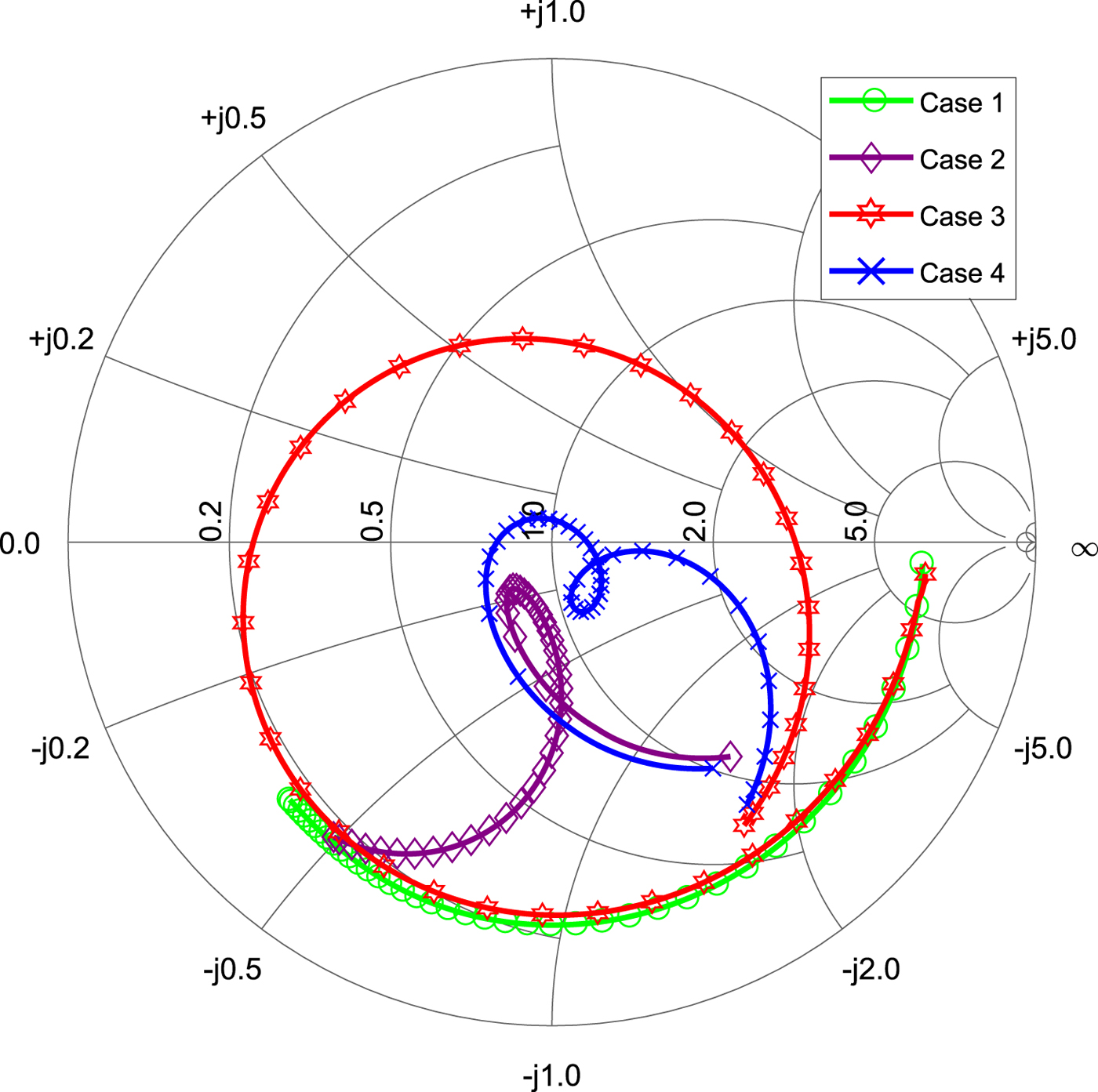
Here, Zπ describes the parallel circuit of the parasitic base-emitter resistance r π with the base-emitter capacitance C π on the CC input. As a result, the resistive part of the feedback branch lowers the real part of Zin for low and medium frequencies as shown in Fig. 7, Case 2. By a careful choice of R f, the input impedance can be shifted near to the matching impedance Z 0 for low and medium frequencies. Furthermore, the shunt feedback (FB1) leads to a more broadband characteristic of the input impedance Zin, what will be apparent from the consideration of Case 2 in Fig. 7. The resulting characteristic of the input matching is shown in Fig. 6, Case 2. For frequencies higher than 23 GHz, the matching is not good enough. To achieve a more broadband matching, an additional LC-network is implemented at the input, which forms together with Zin and the impedance of the feedback branch a π-network. The LC-network consists of the inductor L 1 and the MIM capacitor C 1. The π-network influences the matching only in a limited range, as can be seen in Fig. 6. The red curve (Case 3) shows the simulated influence of the π-network in absence of the feedback branches. It consists in the simulated case only of the MIM capacitor C 1, the inductor L 1 and the parasitic base-emitter capacitance of the common emitter transistors T1 and T2, respectively. In the realized circuit, the capacitive behavior of the feedback branches has an impact to the overall capacitance of the π-network’s branch at the input node of the CC. Furthermore, it is obvious from Fig. 6, Case 3 that the π-network is tuned in this way that its influence to the matching function appears in the frequency range from 15 to 40 GHz. The goal of the additional LC-circuit at the LNA’s input is to compensate the capacitive characteristics of the CC with a shunt feedback to a certain extend and additionally move the resistive part of Zin more to the optimal matching point. Both effects of the additional LC-network can be seen in Case 3 in Fig. 7, where only the LC-network is implemented at the LNA’s input without the feedback branches. For low frequencies, the LC-network does not have an effect in this constellation. The plotted curves in Fig. 6, Case 4 and in Fig. 7, Case 4, show the resulting matching of the LNA, when both methods are implemented. Unlike the traditional implementation of the shunt feedback (FB1), the MIM capacitor C f in the feedback branch is not only implemented to separate the input- and the output-biasing. In this case, its value would be very high. For the presented LNA, the value of the capacitor C f is chosen around C f = 200 fF. This value was carefully chosen during the design process to place the zeros in the linear matching function in this manner that the matching is best over the desired frequency range.
Extended variable gain control circuit
In the proposed design, the standard CC topology is enhanced with a special circuit (see three dotted boxes named with FB2 and VGC in Fig. 3), which provide an adjustable variable gain and make sure that the input matching is good for all gain levels over a wide frequency range. This behavior is reached due to the additional shunt feedback (FB2) in the gain control branch, which is shown in Fig. 3 in the left and right dotted box. To improve the isolation inside the VNA, a second VGC circuit (VGC_EF) is implemented in the emitter follower output stage of the LNA, as shown in Fig. 3 on the left- and right-side.
The reason for the need of the additional shunt feedback branch (FB2) in the VGC circuit becomes clear by a closer view on the mechanism, which occurs if the transistors T5 & T6 of the VGC circuits become conductive. By becoming a lower load impedance for the common emitter transistors T1 & T2, the gain of the CC decreases. Because of the strong effect of the shunt feedback on the input impedance Zin, the matching would also be hardly degraded, if the feedback branch becomes more and more ineffective, when the current through the upper part of the CC is shifted into the VGC circuit. To compensate the declining effect of the original shunt feedback (FB1), a second feedback branch (FB2) is implemented from VGC circuit to the base node of the common emitter transistor of the CC. The values of the resistor and the capacitance of the second feedback (FB2) are equal to the ones of feedback (FB1). The additional feedback (FB2) is implement on both half-circuits of the differential CC. To keep the influence of the feedback branch on the input impedance relatively constant over all gain levels, the values of the resistors at the collectors of transistors T5 & T6 are equal to the value of the resistors R L on top of the cascode. The measured results are shown in the next chapter.
Stability of the LNA circuit
The impedance of a DUT, which is measured with the monolithic integrated VNA, is not in every case 50 Ω. Therefore, it can cause instabilities inside the LNA. To ensure that the LNA is stable under all possible load conditions, the K-Factor method, sometimes called the Rollet-Factor, is an often used method. The DUT connected to the LNA’s input can cause instability if the LNA is not unconditionally stable. The output load connected to the LNA can cause instability as well, if the LNA is not stable under all conditions. Especially, the use of an EF as output stage of the LNA, that acts as bandwidth extension in the before described manner, is a potential source of instability. The reason for this is the resulting RLC-resonant behavior, as mentioned above. The used MIM-capacitor at the output of the EF has a major impact to the resonant behavior of the EF. Its value must carefully be chosen. Together with the inductance of the connection lines, it can lead to oscillations and as a result, the whole circuit becomes unstable [Reference Trotta, Knapp, Aufinger, Meister, Böck, Dehlink, Simbürger and Scholtz9]. To avoid this, the connection between the CC’s output and the input of the EF is made as short as possible, to reduce the parasitic inductance to a minimum. This avoids possible oscillations, if the connection is short enough. With K-Factor simulations, the stability is checked. The results can be seen in Fig. 17 in the section “Characterization results”. As explained in [Reference Ellinger11, Reference Rollet12], the circuit is unconditionally stable, if the criteria
 $$ K \gt 1, \; \bigl\vert \underline{S}_{11}\bigl\vert \lt1 \quad {\rm and} \quad \bigl\vert \underline{S}_{22}\bigl\vert \lt1, $$
are fulfilled. Because the Rollet-Factor determines only instabilities caused by external loads, a further analysis is necessary to detect instabilities, which are caused through slightly negative impedances inside a stacked topology like the CC. The CC is potentially unstable, because of its CB transistor on its top. So, special care is spent, to ensure a low ohmic AC-coupled connection to ground.
To detect instabilities inside the stacked CC circuit, without affecting it, a special tool is necessary, the so-called S-Probe stability simulation [Reference Schmid, Coen, Shankar and Cressler13]. The results of the S-Probe check at the base node of the CB transistors can be seen in Fig. 18 in the section “Characterization results”.
Influence of process-tolerances
In the fabrication process, the values of the single components inside the chip vary from their ideal value, which were used in the simulation. Two reasons are responsible for that. The first and most powerful reason is the process variation over the wafer. Therefore, chips from far separated places on the wafer exhibit strongly different deviations from the ideal value. Especially for components like resistors and capacitors, the variation can be far more than ±10%. This leads to variations in the performance parameters of the realized circuit. The second source of process tolerances are the deviations between components inside a single chip, the so-called “mismatch”. They are less strong than the process variations, but due to the fact that both types of variation occur during the fabrication process, the overall tolerances depend on both. The effect of these two variations on the performance parameters can be determined through a Monte Carlo (MC) simulation.
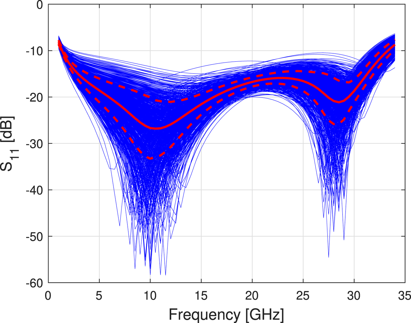
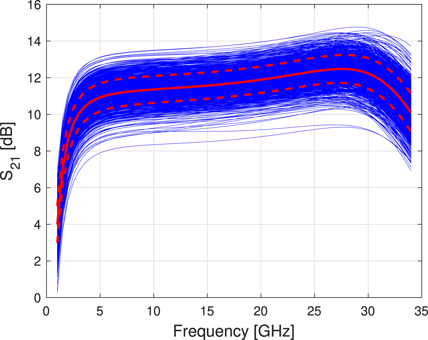
The MC simulation is done with 1000 sweeps. Both types of variations are done at the same time. In Fig. 8, the result of the MC simulation for the S 11-parameter is shown. For the correct interpretation of the simulation results, it is important to note that the density of the different S 11-plots is not the same along the y-axis. Therefore, the probability becomes less to the vertical edges of the family of curves. To make this visually clear, the mean-value is calculated and plotted for each simulated frequency point. The red thick solid curve shows the mean values. As a value for the ordinary deviations, the standard deviation was calculated for each simulated frequency point over the family of curves and is plotted in the diagram as red dotted curve. The key information, which can be extracted from Fig. 8, is that the matching limit of −10 dB over the desired bandwidth can be adhered. As explained before on the input matching, a MC simulation is also done on the parameter S 21. The result of the MC simulation of the gain S 21 of the LNA is shown in Fig. 9. With the help of the standard deviation and the mean-value, the key information can be extracted that the gain of the LNA varies usually ±1 dB around the mean value.
Monte Carlo simulation of the input matching S 11 in [dB] over process- and mismatch-variations. The Monte Carlo simulation contains 1000 sweeps.
Monte Carlo simulation of the LNA's gain S 21 in [dB] over process- and mismatch-variations. The Monte Carlo simulation contains 1000 sweeps.
RF downconverter
The second key component in the RX Chain of a VNA is the RF Downconverter, which has a lot of influence on the measurement performance of the VNA. The RF Downconverter consists of a Gilbert Mixer with an additional output buffer, as can be seen in Fig. 10. Besides the high CG, which can be achieved with this topology of an active mixer, the double balanced architecture allows a powerful common-mode rejection. In the context of a Multi-Port VNA, it is very important to get a very high isolation between the measurement channels.
Simplified schematic of the RF-Downconverter without biasing. On the right side, the IF buffer is shown.
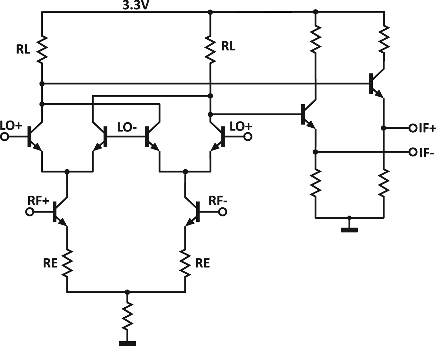
Besides the core of the Gilbert Mixer, the output buffer is depicted on the right side of Fig. 10. The buffer improves the gain of the basic mixer core through its high input impedance, because it is in parallel to the load resistors of the Gilbert Mixer. The mixer load itself is realized without the typical parallel MIM capacitors and spiral inductors. These components would result in a strong limitation of the mixer bandwidth. The RF Stage of the Gilbert Mixer has two additional TaN resistors R E for emitter degeneration. This helps to flatten the CG.
One important property for the performance of the VNA is the gain of the measurement receiver paths, because the gain influences directly the sensitivity of the VNA. The CG itself inside the mixer is mainly determined throughout the mixer’s RF-stage, which is in a typical Gilbert Mixer a differential pair. A simplified description of the available CG of the Gilbert Mixer can be given according to [Reference Voinigescu14] by the following equation (12).
 $$ A_V = - {\displaystyle{2} \over{\pi}}\cdot {\displaystyle{g_{m\_DiffPair}} \over {1+g_{m\_DiffPair}\cdot R_E}}\cdot R_L $$
In equation (12), the resistors R E for the emitter degeneration are taken into account. This reduces the CG by a factor of  $({1}/{(1+g_{m\_DiffPair} \cdot R_E)})$, but improves the linearity of the mixer. In equation (12), a perfect LO square waveform is assumed, which excites the LO switching quad as perfect switches, with an infinitely high slew-rate. For sinusoidal waveforms, as they are typically produced by integrated RF oscillators, the slew rate is lower than for square signals. This leads to a small time frame ΔT per half-wave, where all transistors of the switching-quad are conductive [Reference Razavi15]. In this time frame, the small signal current of the RF stage is split into equal portions. Therefore, in the time frame ΔT most of the input signal is converted from differential-mode into common-mode. Thus, for ΔT, no gain is produced on the balanced output node of the differential pair on the RF-Port. To overcome this gain reduction to a large extent, a high amplitude for the LO driving-signal has to be applied, to achieve a high slew-rate. Therefore, the optimal power level for the LO-signal has to be determined. The optimal power level is measured and is shown in the following chapter “Characterization results” section “Optimal LO power level”.
Characterization results
Setup for single-ended measurements
For characterization, a Keysight PNA-X vectorial network analyzer is used in combination with Z-Probes with 100 μm pitch and GSGSG-pinning. The measurements are done in single-ended configuration, as well as the simulation of the CG, whereas NF and P1dB are simulated in a balanced configuration. The intermediate frequency is 1 GHz. The characterization of the receiver chain is done by the Scalar Mixer (SMC) measurement, which is implemented as an option in the PNA-X. The SMC measurement considers in contrast to a normal S-Parameter measurement the frequency translation between the input and the output of the receiver. In the SMC option, standard S-Parameters S 11 and S 22 are measured for determining the matching, whereas the CG according to [Reference Dunsmore5] is determined by the ratio of the following wave portions:
 $$SC_{21}= {{\displaystyle{\left\vert b_{2\_OutputFreq}\right\vert} \over{\left\vert a_{1\_InputFreq}\right\vert}} \bigg\vert _{a_{2 \_ OutputFreq=0}}}.$$
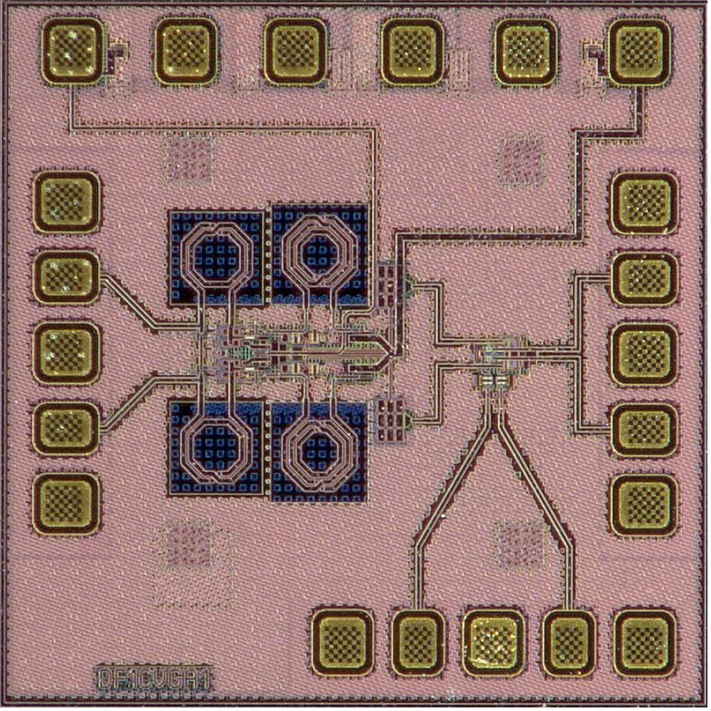
In equation (13),  $b_{2\_OutputFreq}$ is the outgoing wave portion of the IF-Port of the receiver on the IF frequency and $a_{1\_InputFreq}$ the ingoing wave portion on the RF-Port of the receiver on the RF-Frequency. The calibration of the SMC measurement is done in two steps [Reference Dunsmore5]. In the first step a power calibration of the LO-, RF- and IF-Port is done, to adjust the power level on the respective reference plane, as well as to calibrate the PNA-X’s reference receiver to the respective reference plane’s power level [Reference Dunsmore5]. In the second step, a TOSM calibration of the RF- and IF-Port is carried out. The respective reference plane is set to the tips of the Z-Probes. The chip photo is shown in Fig. 11. The outer dimensions of the fabricated chip are 928 × 928 μm.
Chip photo of the designed broadband receiver. The outer dimensions of the fabricated stand-alone chip are 928×928 µm.
Conversion gain and input-matching
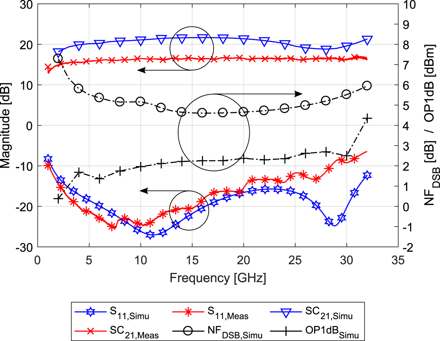
Figure 12 shows the measured conversion gain SC 21 and the input matching S 11 of the receiver chain chip. The CG is greater than 15 dB over a frequency range from 2.1 up to 32 GHz and the 3 dB-criterion is met from 1 GHz on. The input matching is better than − 10 dB from 1 to 28 GHz, which is very important for a network analyzer, because calibration and measurement results of the integrated VNA are much more accurate if the input matching is good. The comparison of the measured input matching with the simulated one shows a good agreement in the range between 1 and 25 GHz. Above this frequency range, the geometry of the input transmission lines has an effect, because in simulation the cavity around the input spiral inductors was not considered.
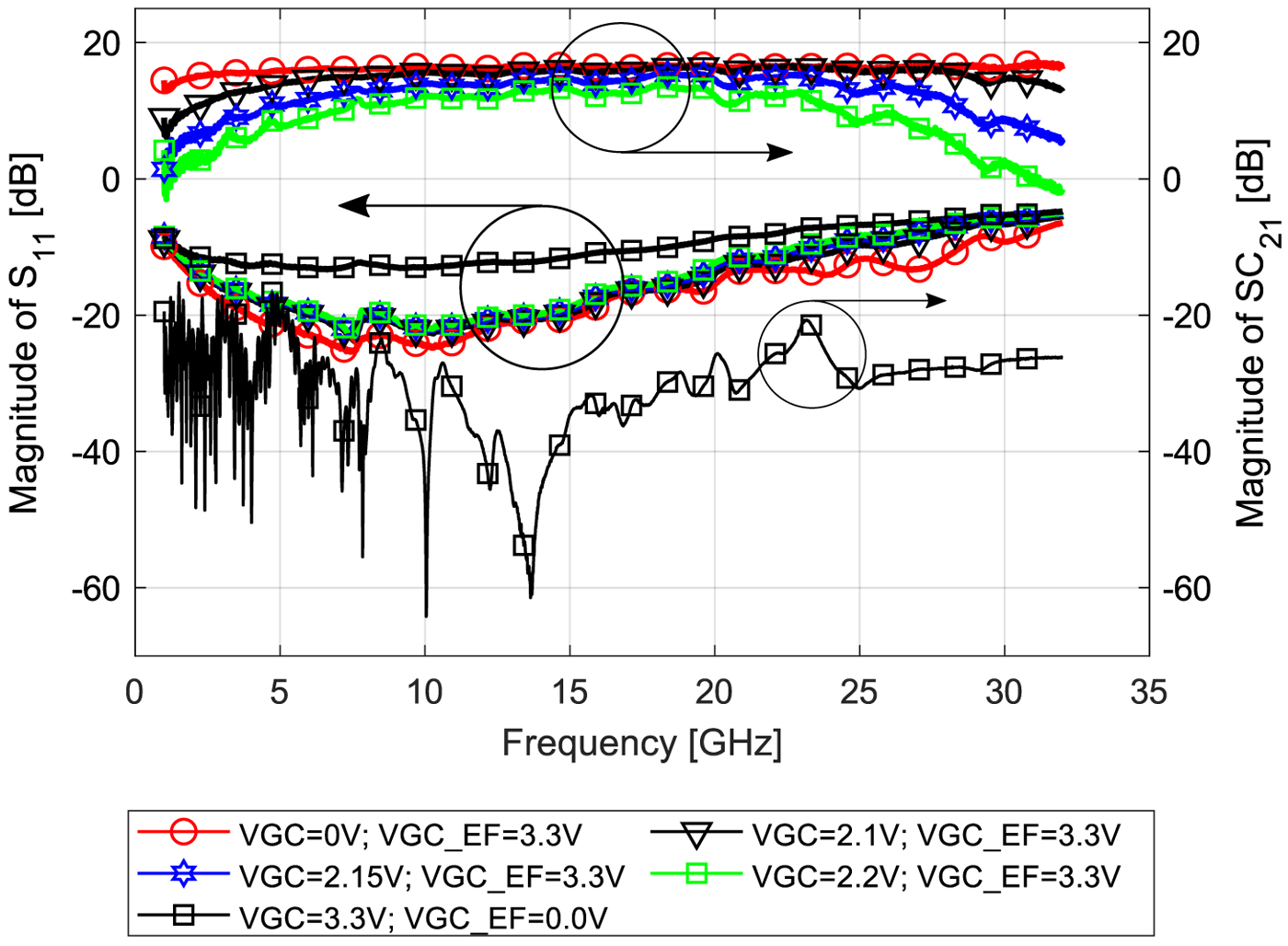
Figure 13 shows the resulting input matching for different gain levels, as well as the resulting CG. Furthermore, Fig. 13 shows an additional isolation through the deactivated EF of the LNA. The measurement results in Fig. 13 shows a matching better than − 10 dB up to 18 GHz for all gain levels, which is reached through the additional shunt feedback extension (FB2) in the VGC circuit (see Fig. 3). This is very important to avoid reflections back to sensitive materials under test.
Characteristics of the whole receiver chain. S 11,Meas describes the measured input matching and SC 21,Meas the measured conversion gain. Additionally, the simulated input matching S 11,Simu and the simulated gain function S 21,Simu are shown. Finally, the simulated Double-Side Band (DSB) noise figure NF DSB,Simu and the simulated output referred compression point OP1dB Simu are shown.
Measurement results of input matching S 11 and conversion gain SC 21 for various gain control levels VGC of the CC circuit of the LNA and VGC_EF of the EF output stage of the LNA.
Simulation results of noise figure and compression point
In Fig. 12, the simulated noise figure (NFDSB) and the simulated output-referred 1 dB compression point (P1dB) are shown. In case of the NF, the values are between 4.6 and 5.8 dB for 4–32 GHz. The values of P1 dB are between 0.1 and 4.3 dBm in the frequency range from 2 to 32 GHz.
Optimal LO power level
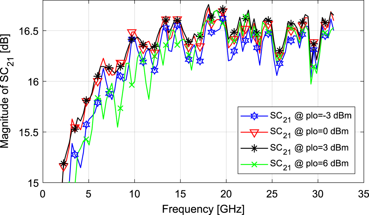
The power level of the LO-Signal has an impact on both, the CG and the noise figure (NFM) of the downconversion mixer. Therefore, the optimal LO power has to be determined. In Fig. 14, the conversion gain SC 21 of the receiver for various power levels is shown. The optimum conversion is reached for power levels between 3 and 6 dBm. For lower power levels, as well as for higher power levels, the conversion degrades.
Measured conversion gain SC 21 for various power levels on the LO-Port.
Isolation
In the following, the results of the isolation measurements are presented. In detail, the LO-to-RF isolation, the RF-to-LO isolation and LO-to-IF isolation. Before the results are presented, the measurement setup, as well as the calibration, is explained.
Measurement setup
The measurement of the receiver’s isolation requires a true differential excitation of the receiver’s ports. This means, that a single-ended measurement with a subsequent conversion from nodal into modal S-Parameters is not sufficient in this case. The reason is that the used Gilbert Mixer only works as a double balanced downconverter, if the switching quad is driven with a fully differential signal. The common use of a balun is not preferable in this case, because of the high input bandwidth of the receiver chain. A balun would generate mode conversion, because of its not perfect symmetry over the whole bandwidth. The measurements are done with a Keysight PNA-X with iTMSA-Option (Integrated True Mode Stimulus Application), which is implemented in firmware Option 460. This option allows the interconnection of the two internal sources of the PNA-X to one balanced source. With the help of this interconnection, two balanced ports can be realized. Therefore, the modal S-Parameters can be measured directly and furthermore, the correct excitation of the Gilbert Mixer is possible.
The calibration of an iTMSA-measurement is carried out in three steps. The first step is a power calibration over the whole measurement bandwidth. With a thermal power meter from Rohde & Schwarz & Co. KG (NRP-Z55), the power calibration is done single-ended on source 1 of the PNA-X. In step 2, a 4-Port TOSM-Calibration with a CAL-Substrate is done. By this step, the reference plane is set to the tips of the measuring probes. For the isolation measurement Z-Probes (Z040-K3K) from Cascade Microtech, Inc. are used, which have a pitch of 100 μm and a GSGSG-pinning. According to [Reference Dunsmore5], a third calibration step is necessary, especially for DUTs, which need a perfect differential excitation to have a good differential mode behavior, as well as a good common mode suppression. In general, a symmetrical differential excitation can become unsymmetrical through a not perfect matching, layout inaccuracies or inaccurate contacting [Reference Dunsmore5]. This leads to a phase-skew, which has to be compensated. For determining the phase-skew, on each of the two balanced ports, a sweep of the phase is done in this way that only one of the two single-ended ports of a balanced port is swept in its phase, whereas the other is fixed in its phase. The phase-sweep is done with the highest frequency of the operating band of the receiver chain. By means of the highest isolation, which occurs over the phase-sweep, the deviation of relative phase to the ideal phase-offset of 180° between the two single-ended ports of a balanced port can be determined. The determined phase-skew of the DUT is inserted as an offset in the iTMSA-option of the PNA-X. The proposed receiver did not exhibit any significant phase-skew in the measurement. Therefore, no phase-offset was inserted in the iTMSA-option.
Isolation of LO- to RF-port
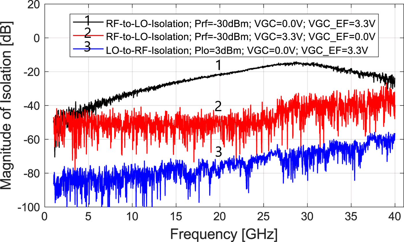
The isolation between the LO-Port and the RF-Port is measured by stimulating the LO-Port with a CW-signal with a power level, which has the same value, as it is used in the normal operating mode. Different to the measurement of the CG, the feedthrough power level of the LO-Signal is measured at the RF-Port at the same frequency. In Fig. 15, the lower curve (3) shows the measured LO-to-RF isolation. The measured isolation for the whole input frequency band is equal or better than 60 dB. Such a high isolation is well suited for the application of a monolithic integrated VNA. The suppression of the LO-Signal on the RF-Port is very important to avoid self-mixing of the LO on a poorly matched DUT, which is measured with the integrated VNA. Furthermore, the feedthrough of the RF signal to the LO-Port is measured, because this can lead to superposition in the other integrated VNA channels, since all LO-Ports are connected via a LO distribution network. Especially, a superposition with the reference channel would falsify the measurement results of the monolithic integrated VNA. In Fig. 15, the middle curve (2) shows the measured isolation from RF-Port to LO-Port, for the case that the gain of the LNA is set to its minimum. This means that the gain control voltage VGC (see Fig. 3) is set to 3.3 V and the Emitter Follower is fully disabled (VGC_EF = 0 V). The RF-to-LO isolation is better than 30 dB over the whole input bandwidth. For the low and middle frequency range up to 26 GHz, the isolation is better than 40 dB. As a result, the enhanced gain control function improves the isolation for a disabled measurement channel in the integrated VNA. For the case that the gain of the LNA is set to its maximum, the EF of the LNA is enabled (VGC_EF = 3.3 V), as well as the gain control voltage of the CC has to be set to VGC = 0 V. The resulting RF-to-LO isolation seems to be worse, as can be observed in Fig. 15 at the upper curve (1). But here, the gain of the LNA must be taken into account, which leads to a stronger RF signal on the downconverter’s RF-Port. With an input power of −30 dBm on the LNA and the maximum gain level of the LNA, the isolation is better than 20 dB for frequencies below 22 GHz and reaches its minimum of 15 dB at around 28 GHz.
Measurement results of isolation between LO- and RF-Port and vice versa.
Isolation of LO- to IF-port
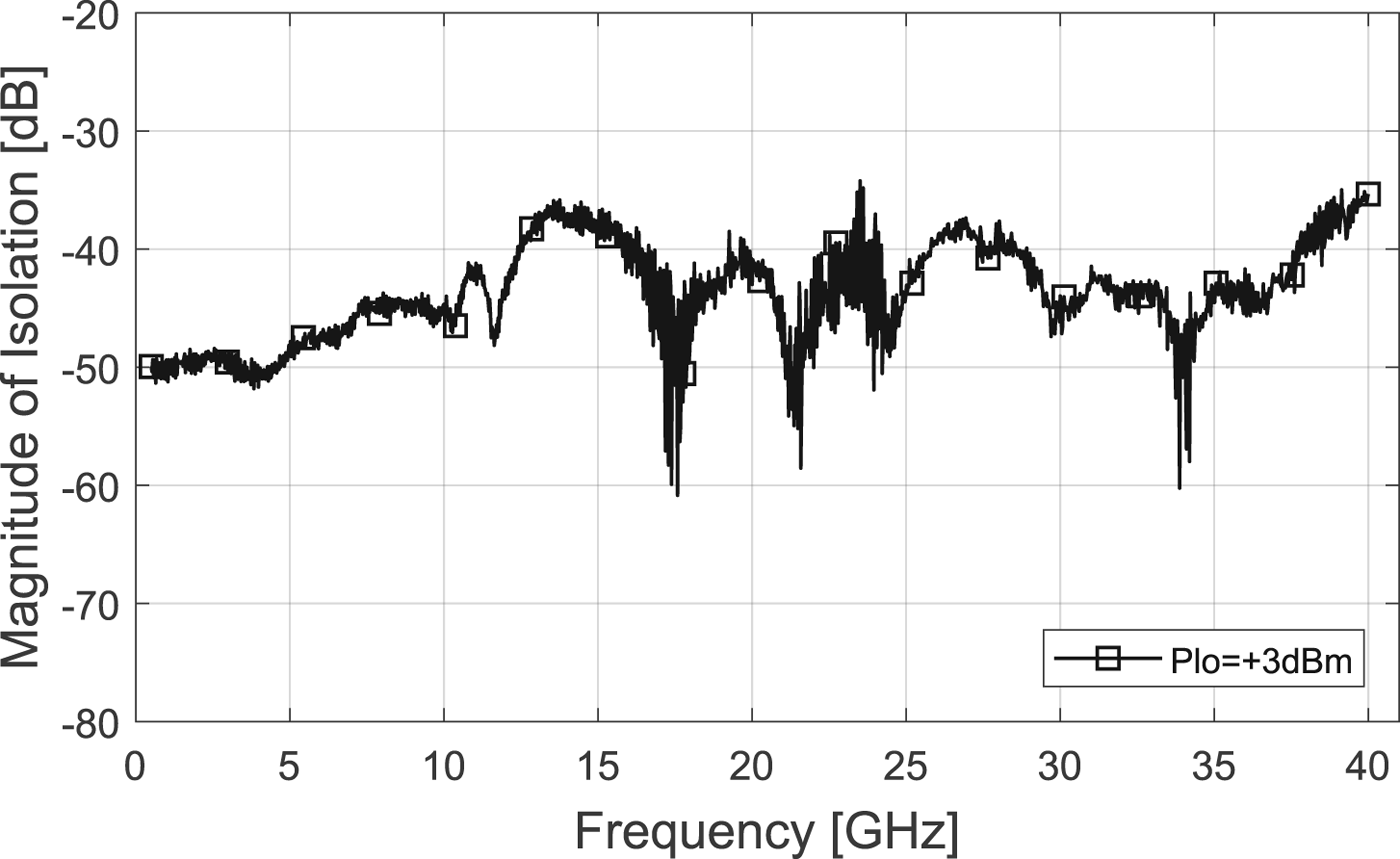
A further important feedthrough path is from LO- to IF-Port. Especially, for low measurement frequencies of the monolithic integrated VNA, where the LO frequency has only a small distance to the IF frequency in the spectrum, it is difficult to filter out the harmonics of the LO-Signal. This results in an impure output spectrum, which degrades the measurement performance of the integrated VNA significantly. Therefore, the LO-to-IF isolation has to be as high as possible. In Fig. 16, the measured isolation between the LO- and the IF-Port is shown. Over the whole LO frequency band the isolation is better than 35 dB. The LO power, which was used for the measurement, is 3 dBm on the balanced port.
Measurement results of isolation between LO- and IF-Port.
Stability analysis
K-factor analysis
According to [Reference Ellinger11, Reference Rollet12] the K-factor can be determined out of the measured or simulated S-Parameters. The K-factor can be expressed according to [Reference Ellinger11, Reference Rollet12] by
 $$K={\displaystyle{1- \vert\underline{S}_{11}\vert^2-\vert\underline{S}_{22}\vert^2 + \vert {\rm det}\underline{\bf\,{S}}\vert^2} \over{2 \vert\underline{S}_{12}\underline{S}_{21}\vert}}, $$
with
 $$ \det\underline{\bf\,{S}}=\underline{S}_{11}\underline{S}_{22}-\underline{S}_{12}\underline{S}_{21}. $$
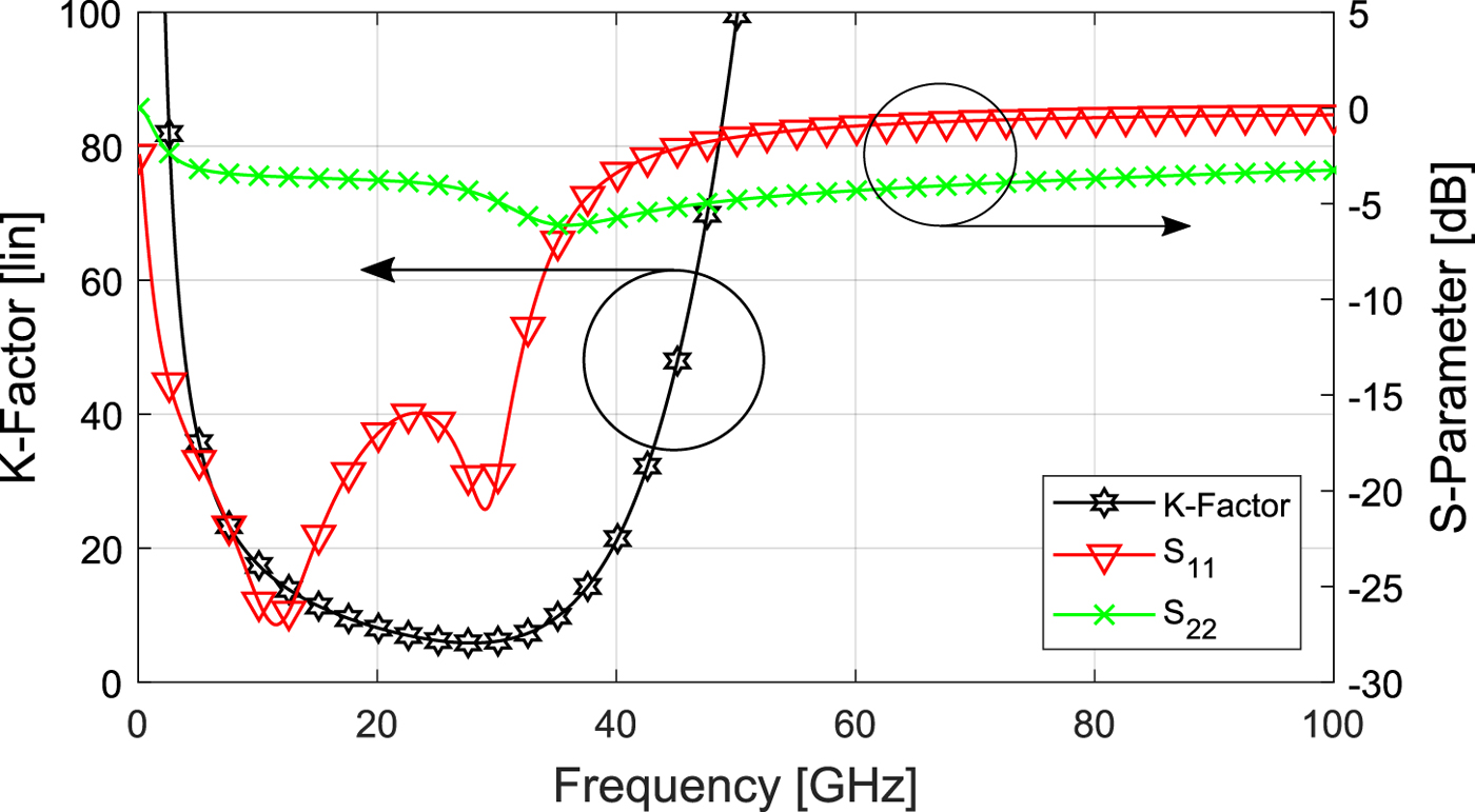
The simulation results in Fig. 17 show that the LNA is unconditionally stable over the used frequency range, because the conditions in equation (11) are met for all frequencies.
The test is done for a frequency range of 100 MHz up to 100 GHz to ensure, that neither the relevant higher harmonics nor subharmonics can cause an instability. Note, that in Fig. 17 the K-Factor for high frequencies is too high for plotting, but it is simulated until 100 GHz.
Results of the simulative stability test with K-factor method of the LNA.
S-probe analysis
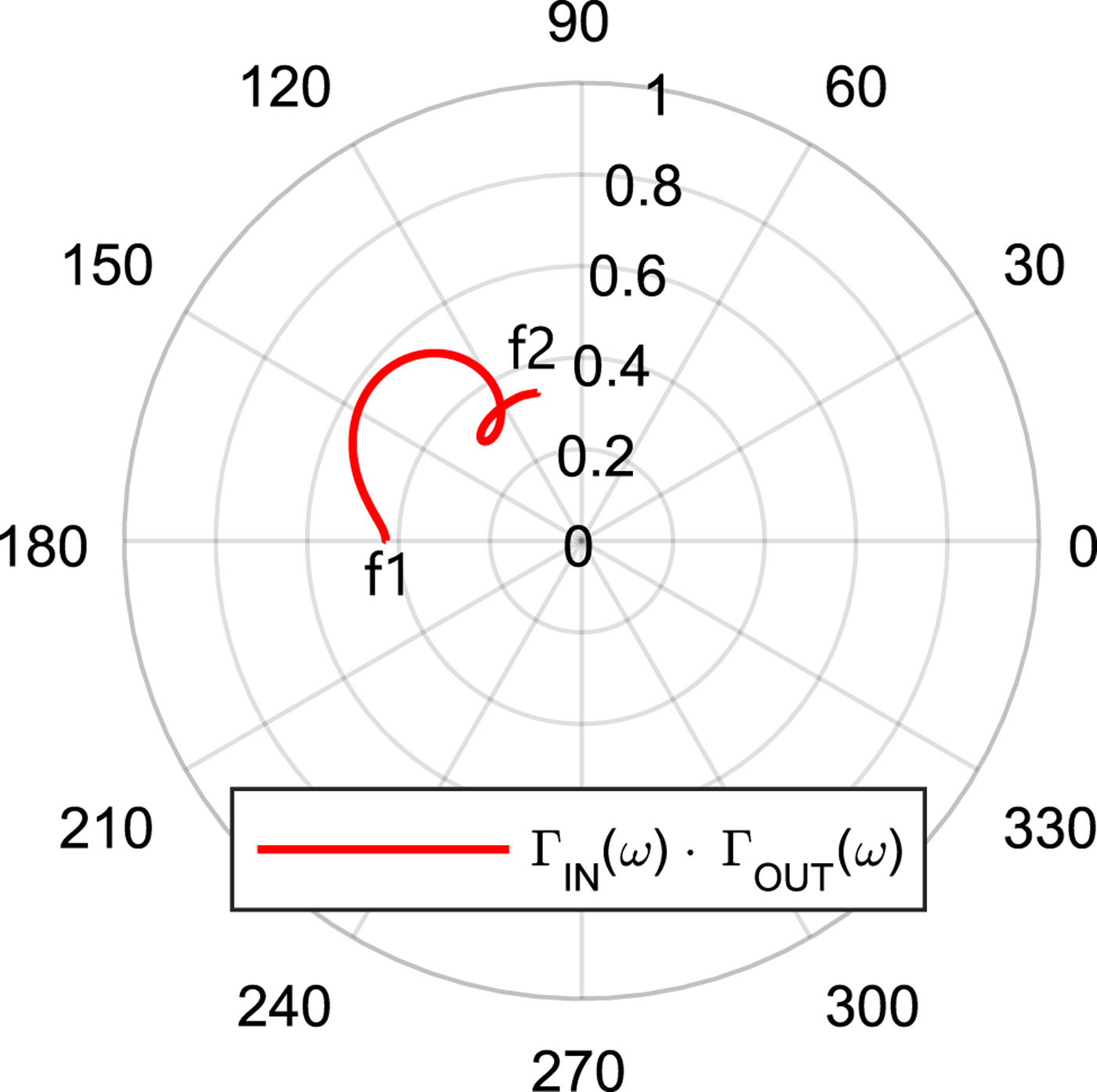
With the help of the S-Probe, the input reflection coefficient ΓIN(ω) and the output reflection coefficient ΓOUT(ω) can be determined for every node inside a circuit without split up the single parts. Finally, by using the simulated reflection coefficients ΓIN(ω) and ΓOUT(ω), the Nyquist stability criterion can be determined over frequency. For this purpose, the product of ΓIN(ω) · ΓOUT(ω) has to be plotted. If the resulting curve encircles the point (1,0) clockwise, this indicates an instability. This is equivalent to poles in the right-half plane in the Pole-Zero-Plots, as it is typical for oscillators. In Fig. 18, the results of the stability test with the differential S-Probe is shown. Because the plotted product of ΓIN(ω) · ΓOUT(ω) does not nearly encircle clockwise the point (1,0) for any frequency, the tested node is stable.
Results of the simulative stability test with a differential S-Probe, at the base node of the CB transistors of the CC inside the LNA. The stability test was done from f1 = 100 MHz to f2 = 100 GHz.
State-of-the-art comparison
The results are compared in Table 1 with some previous designs of other authors.
Comparison of the receiver chain with previous works
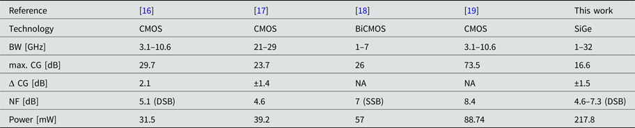
The bandwidth of over five octaves is outstanding compared with [Reference Shi and Chia16–Reference Park, Lee, Choi and Hong19]. Furthermore, the max. gain deviation is comparable to the other designs, but over a much wider frequency range. The measured current consumption at a supply voltage of 3.3 V has a value of 66 mA, which is higher compared with the power consumption of the designs of the other authors. A reason is that in [Reference Shi and Chia16, Reference Lin, Lee, Huang, Wang, Wang and Lu17] the LNA is in both cases single-ended, whereas the LNA in this work is fully differential. The noise figure (NF) is between approximately 12 and 26 GHz better, compared with [Reference Shi and Chia16], but outside this frequency range a little bit higher. In contrast to [Reference Park, Lee, Choi and Hong19], the NF is better over the comparable frequency range. The designs in [Reference Shi and Chia16, Reference Joram, Wagner, Sobotta and Ellinger18] show better noise performance for the frequency range up to 7 and 11 GHz, respectively, which can be explained in both cases by the higher gain. The CG itself is less than in the other designs [Reference Shi and Chia16–Reference Park, Lee, Choi and Hong19]. The reason is the enormously expanded bandwidth, which reduces the gain of the LNA through the gain-bandwidth product.
Conclusion
A multi-octave receiver chain has been presented, which is well suited for a front-end of a monolithic integrated vector analyzer. For this application, the key performance parameters of the receiver chain have been highlighted and the necessary design methodology and topology enhancements have been shown in detail, which are necessary to achieve such an enormous bandwidth of five octaves. The result is a CG of max. 16.6 dB, with a very flat deviation and an enormous 3 dB-bandwidth from 1 to 32 GHz. The input matching is better than −10 dB up to 28 GHz. The NF is between 4.6 and 5.8 dB for 4 to 32 GHz and the output referred 1-dB-compression-point is from 0.1 to 4.3 dBm between 2 to 32 GHz. Especially, an enhanced VGC circuit has been proposed, which enables the handling of measurement signals with strongly different power levels and provides at the same time a good matching that avoids reflections back to sensitive materials under test. This prevents a falsification of the determined S-Parameters of the material under test. Furthermore, a second gain control functionality has been implemented to improve the isolation of the deactivated chains in the VNA. The measured RF-to-LO isolation is 40 dB up to 26 GHz and 30 dB for higher input frequencies. Additionally, the LO-to-RF isolation is higher than 60 dB for the complete frequency range, which is a very good value. The measured LO-to-IF isolation is better than 35 dB over the complete bandwidth. A special focus has been laid on the measurement setup for the determination of the isolation of the fully differential receiver chain. Finally, the influence of the fabrication tolerances onto the performance parameters has been investigated, as well as the optimal LO power level. The proposed fully differential integrated receiver chain allows very broadband integrated VNAs.
 Marco Dietz received the B.E. degree in communications engineering from the Ulm University of Applied Sciences, Ulm, Germany, in 2011, and the M.Sc. degree in electrical engineering (with a focus on high-frequency engineering and microelectronics) from Friedrich-Alexander-University Erlangen-Nuremberg, Erlangen, Germany, in 2013. In 2014, he joined the Institute for Electronics Engineering, Friedrich-Alexander-University Erlangen-Nuremberg, as a Research Assistant, where he is currently a member of the Team RF Integrated Systems. Since 2015, he has been the Head of the Team. His current research interests include high integrated, silicon-based microwave circuits and systems with multi-octave bandwidth for material characterization and wireless sensor and communication systems for ultra-low power, industrial and biomedical applications. Mr. Dietz received in 2014 one of the IHP-Young-Talent-Awards, sponsored by Freunde des IHP e.V., for his master thesis.
 Andreas Bauch studied electronics engineering at the University of Erlangen-Nuremberg, Germany from 2008 to 2013. He received his M.Sc. degree in electrical, electronic and communications engineering from the University of Erlangen-Nuremberg, Germany, in 2013. In 2013, he joined the Institute for Electronics Engineering, Erlangen, Germany, as a Research Assistant and is currently pursuing his Ph.D. His working fields cover millimeter wave, RF and integrated circuits.
 Klaus Aufinger received the Diploma and Ph.D. degrees in physics from the University of Innsbruck, Innsbruck, Austria, in 1990 and 2001, respectively. From 1990 to 1991, he was a Teaching Assistant with the Institute of Theoretical Physics, University of Innsbruck. In 1991, he joined the Corporate Research and Development of Siemens AG, Munich, Germany, where he investigated noise in submicrometer bipolar transistors. He is currently with Infineon Technologies AG, Neubiberg, Germany, where he is involved with device physics, technology development, and the modeling of advanced SiGe technologies for high-speed digital and analog circuits.
 Robert Weigel received the Dr.-Ing. and the Dr.-Ing. habil. degrees, both in electrical engineering and computer science, from the Munich University of Technology in Germany where he respectively was a Research Engineer, a Senior Research Engineer, and a Professor for RF Circuits and Systems until 1996. From 1996 to 2002, he has been Director of the Institute for Communications and Information Engineering at the University of Linz, Austria where, in August 1999, he co-founded the company DICE, devoted to the design of RFICs for mobile radio and MMICs for vehicular radar applications. Since 2002 he is Head of the Institute for Electronics Engineering at the University of Erlangen-Nuremberg, Germany. Prof. Weigel has been engaged in research and development of microwave theory and techniques, electronic circuits and systems, and communication and sensing systems. In these fields, he has published more than 900 papers.
 Amelie Hagelauer received the Dipl.-Ing. degree in mechatronics and the Dr.-Ing. degree in electrical engineering from the Friedrich-Alexander-University Erlangen-Nuremberg, Erlangen, Germany, in 2007 and 2013, respectively. She joined the Institute for Electronics Engineering of the Friedrich-Alexander-University Erlangen-Nuremberg as a Research Engineer in 2007, where she is involved in SAW/BAW components, RF-MEMS, packaging technologies and integrated circuits up to 180 GHz. Dr. Hagelauer has been the Chair of MTT-2 Microwave Acoustics since 2015. Since 2016 she is leading a research group on Electronic Circuits.



