


Hierarchical materials that can perform seemingly contradicting tasks at multiple length scales are omnipresent in Nature such as strong but tough bone structure, confined but connected brain cells or strong but light spider silk.[Reference Wegst, Bai, Saiz, Tomsia and Ritchie1, Reference Vincent2] However, human-made systems are yet to demonstrate such multifunctionality at multiple length scales.[Reference Wegst, Bai, Saiz, Tomsia and Ritchie1] The attention so far has been given to the investigation and understanding of nanomaterials, and only recently we have started to explore the interconnections of these low-dimensional materials.[Reference Ilday, Ilday, Hübner, Prosa, Martin, Nogay, Kabacelik, Mics, Bonn, Turchinovich, Toffoli, Toffoli, Friedrich, Schmidt, Heinig and Turan3–Reference Escarcega-Bobadilla, Zelada-Guillen, Pyrlin, Wegrzyn, Ramos, Gimenez, Stewart, Maier and Kleij5] We now know that shape and size of the nanomaterials significantly alter their optical, electrical, magnetic, and structural properties; however, there is a whole new paradigm when they organize hierarchically and interconnect in such a way to form multiscale topologies.[Reference Ilday, Ilday, Hübner, Prosa, Martin, Nogay, Kabacelik, Mics, Bonn, Turchinovich, Toffoli, Toffoli, Friedrich, Schmidt, Heinig and Turan3, Reference Escarcega-Bobadilla, Zelada-Guillen, Pyrlin, Wegrzyn, Ramos, Gimenez, Stewart, Maier and Kleij5] If designed carefully, such multiscale topologies could have significant implications for nanotechnology by operating at vastly different length scales from nano to macro. Needless to say, the potential use of these complex structures with topology-dependent features in many applications rely on our ability to understand and control the electronic, optical, magnetic, and chemical interactions between the individual nanostructures along with our capability to exploit their collective properties. However, not only the demonstrations of such complex topologies are very rare, but also their scale-dependent features are poorly understood.
Recently, we have demonstrated such a multiscale, hierarchical complex structure, an anisotropic random network of silicon quantum dots (QDs), to be potentially used in solar cells.[Reference Ilday, Ilday, Hübner, Prosa, Martin, Nogay, Kabacelik, Mics, Bonn, Turchinovich, Toffoli, Toffoli, Friedrich, Schmidt, Heinig and Turan3] Therefore, the topology was designed to be isotropic on the nanoscale (up to ~10 nm) to preserve tunable band gap feature of the QDs in the visible light range (from ~1.8 to 2.7 eV) and anisotropic on the microscale (over tens to hundreds of nanometers) to electrically percolate these dots (conductivity of ~0.1 S/m) and form heavily undulated and branching nanowire-like structures. Here, we show that this structure has different charge transport characteristics on the nanoscale and on the microscale owing to its unique topology for the charges that are locally generated through the photoelectric effect and for those that are injected externally through the electrodes, respectively. We present extensive optical and electrical analyses to establish microscale and nanoscale charge transport dynamics: (i) Transport for charges that are locally generated through the photoelectric effect are identified using room-temperature photoluminescence (PL) analysis. (ii) Radiative and non-radiative carrier recombination processes are identified through room-temperature PL and electroluminescence (EL) measurements. (iii) Transport for charges that are injected externally through the electrodes is analyzed via EL and current–voltage (I–V) measurements. Our findings strongly suggest that, when optimized, these structures can be a strong candidate for use in photovoltaic device applications. Further, by slightly modifying the topology, we were able to create isolated QD clusters that effectively formed a double-barrier tunneling junction (DBTJ)[Reference Balberg, Savir, Jedrzejewski, Nassiopoulou and Gardelis6–Reference Kastner8] that could store charges.
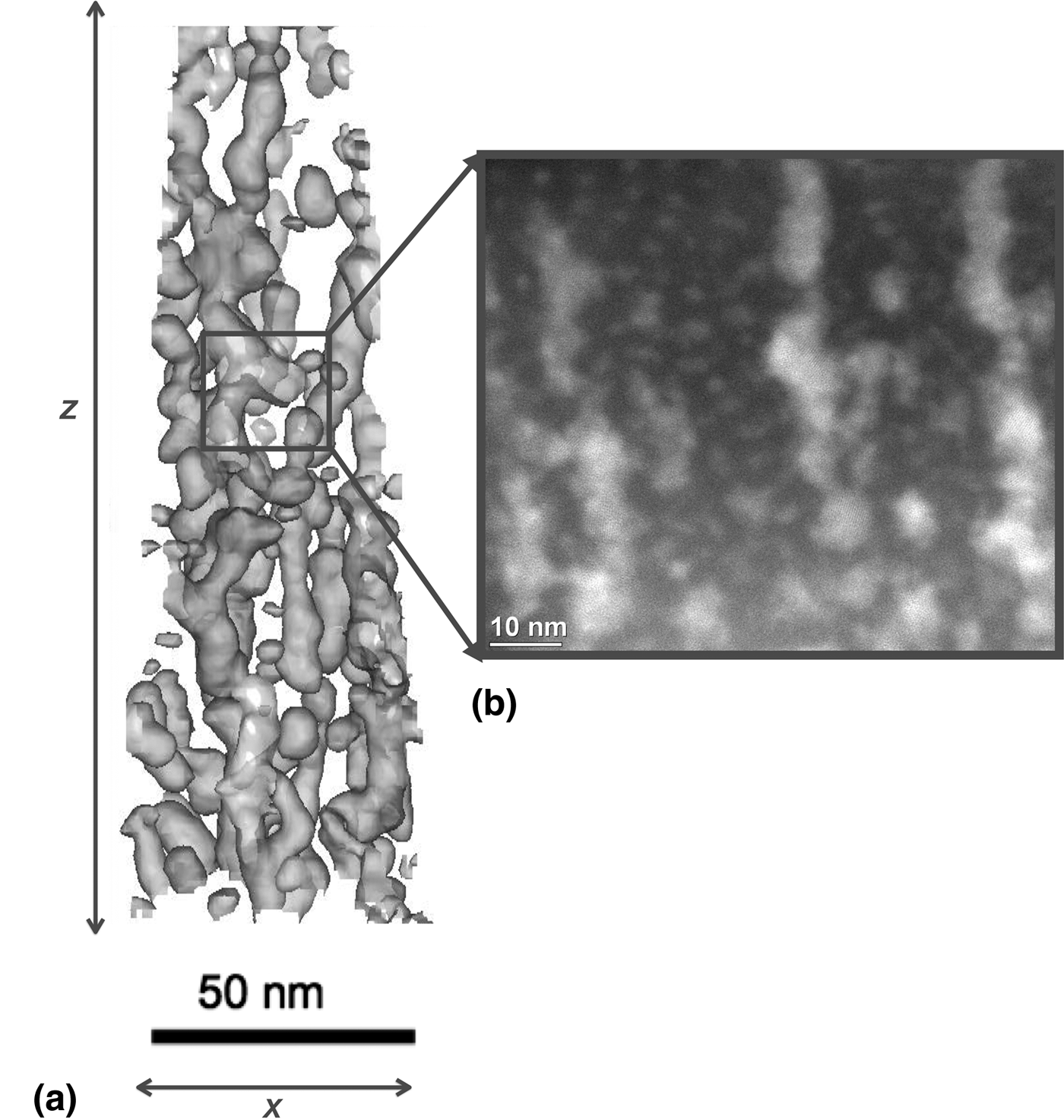
The anisotropic random network is prepared as a thin film in a magnetron-sputtered physical vapor deposition chamber, the details of the fabrication procedure and characterization methods can be found in the Supplementary document. The nanowire-like topology of this random network on the microscale and percolated QD structure on the nanoscale can be seen from the atom probe tomography (APT) and energy-filtered transmission electron microscopy (EFTEM) images shown in Figs. 1(a) and 1(b), respectively. As can be seen in Fig.1(b), the network is entirely composed of nanocrystalline silicon (bright) that is embedded in a dielectric, SiOx matrix (dark). This specific topology can be regarded as a combination of silicon QDs and nanowires, which possess their advantages (i.e. quantum confinement) while overcoming their deficiencies (i.e. large area good electrical conduction). In a solar cell, QDs are generally embedded in a dielectric matrix to provide a potential barrier to creating quantum confinement. However, the same potential barrier that underlies quantum confinement also limits extraction of free carriers from the confined environment and even when they are extracted, the carriers typically have to tunnel through a dielectric medium resulting in a very inefficient current flow.[Reference Gleiter9–Reference Balberg12] Nanowires are almost perfect light-trapping materials owing to their high surface area. They are basically single-crystal materials for which the current flows easily only along the wire.[Reference Priolo, Gregorkiewicz, Galli and Krauss10, Reference Balberg, Jedrzejewski and Savir11, Reference Yan, Gargas and Yang13] However, individual nanowires have to be assembled with high precision to achieve a reasonable conductivity, which is still a big concern.[Reference Balberg, Jedrzejewski and Savir11, Reference Yan, Gargas and Yang13] Random network topology, on the other hand, preserves quantum confinement properties of these two low-dimensional materials while transporting charge carriers within these physically touching, coalescing nanocrystals without the need for them to tunnel through the dielectric matrix.[Reference Ilday, Ilday, Hübner, Prosa, Martin, Nogay, Kabacelik, Mics, Bonn, Turchinovich, Toffoli, Toffoli, Friedrich, Schmidt, Heinig and Turan3] Recently, QD nanowire superlattices have been reported for different material systems,[Reference Zhang and Shi14–Reference Samanta and Das17] where the fabrication is usually a two-step process. First the nanowires are fabricated, and then QD(s) are grown on these nanowires. Often, these multiple steps are performed in different equipments (i.e. atomic layer deposition, metalorganic chemical vapour deposition). On the other hand, fabrication of the random network topology is a single step and simple process, whereby the QDs and nanowires are grown simultaneously, fully integrated and connected in all three dimensions. This full integration allowed us to change the QD diameters within a range of values and to tune the optical band gap of the random network topology. Such a level of integration, connectedness, and control has not been reported in QD nanowire superlattices.
(a) Two-dimensional (2D) projections of 3D APT images of the random network structure. (b) Superposition of the Si (bright) and the SiOx (dark) plasmon EFTEM images showing percolated Si QD network inside a SiOx matrix.
Given the vertically aligned topology of the random network, the majority of the currents are expected to flow in the vertical direction; however, in the lateral direction local current routes are also supposed to contribute to the overall electrical transport. These local routes are quite important for potential photovoltaic device applications: The number of isolated individual and/or clusters of QDs is higher in the lateral direction with respect to those in the vertical direction. This has two important implications: (i) possibility of photocurrent generation when subjected to light illumination, and (ii) possibility of DBTJ formation when isolated individual and/or clusters of QDs are located close enough to the fully connected network.
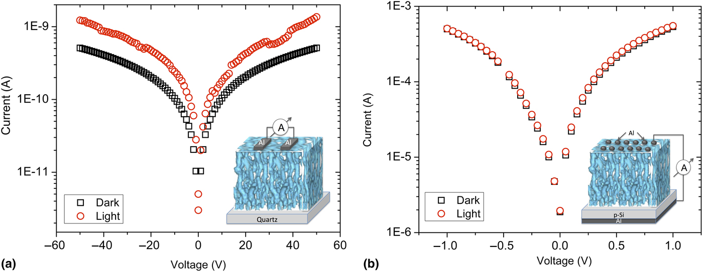
To test the possibility (i), we prepared MOS (metal–oxide–semiconductor) devices [insets of Figs. 2(a) and 2(b)] to perform I–V measurements both in the lateral and in the vertical directions as shown in Figs. 2(a) and 2(b), respectively. As can be seen from these I–V graphs, there is a clear photocurrent generation in the lateral direction [Fig. 2(a)], but in the vertical direction, there is almost no photocurrent generation [Fig. 2(b)]. This observation is quite interesting because it clearly reflects the multifunctional, multiscale topology of this material: when externally induced by a direct current (DC) source, the majority of the currents, whether they are photogenerated or not, pass along the nanowires in the vertical direction, resulting in much higher current flow on the microscale. However, in the lateral direction, on the nanoscale, the topology is isotropic so, there is no directional pathway for the charges to flow along freely. They either have to tunnel through DBTJ configurations (if encountered) or flow through narrow junctions connecting the nanocrystals, where the photocurrent generation is more pronounced.
Graphs show I–V measurements under light-illuminated and dark conditions for the (a) lateral and (b) vertical directions.
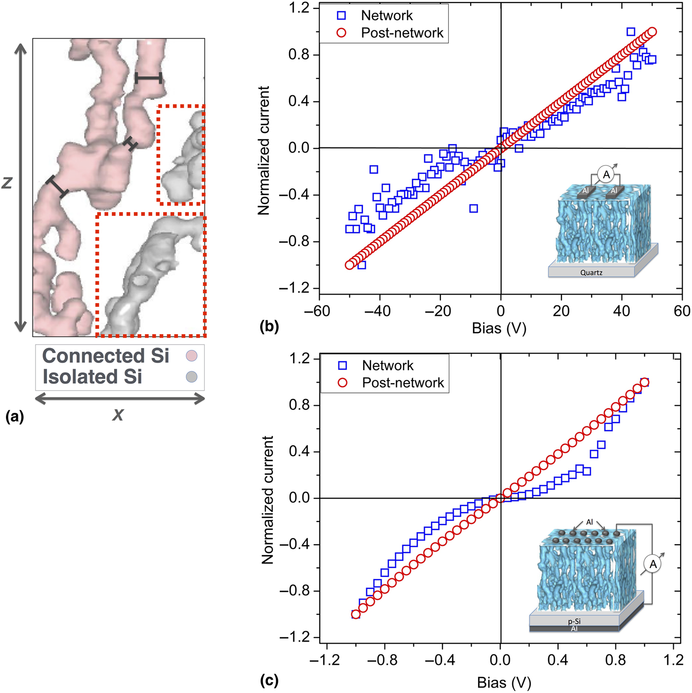
To test the possibility (ii), we performed additional APT analyses [Fig. 3(a)] and identified that there are clusters of QDs that do not touch to the top and bottom electrodes (gray, circled in red dashed lines) inside this fully connected network (pink). Being isolated and located close enough to the fully connected network, these individual and/or clusters of QDs can exhibit Coulomb blockade, which is an effect of the charge quantization that is caused by sequential (non-coherent) tunneling through a small system.[Reference Abeles, Pinch and Gittleman7, Reference Kastner8, Reference Balberg, Jedrzejewski and Savir11, Reference Nie, Petukhova and Kumacheva18] To scrutinize this effect, we have compared I–V measurements of the network structure to that of the post-network structure, where the structure became bulk-like crystalline due to the enlarged sizes of the nanostructures. The subtle, but clear evidence for the Coulomb blockade gap is observed at small bias voltages through the “non-linear” I–V characteristics[Reference Abeles, Pinch and Gittleman7, Reference Kastner8, Reference Balberg, Jedrzejewski and Savir11, Reference Nie, Petukhova and Kumacheva18] as we have shown both in the lateral [Fig. 3(b)] and in the vertical [Fig. 3(c)] directions. It is seen from the graphs that post-network structures do not exhibit such a bias gap since the structure contains a vanishingly small number of isolated clusters or quantum confined structures. In our earlier study, we show through Monte Carlo simulations that the ratio of isolated-to-connected clusters can be controlled just by controlling the Si concentration of the thin film.[Reference Ilday, Ilday, Hübner, Prosa, Martin, Nogay, Kabacelik, Mics, Bonn, Turchinovich, Toffoli, Toffoli, Friedrich, Schmidt, Heinig and Turan3]
(a) APT image shows undulated and branching wire-like morphology of the random network, where the wire diameters differentiate spatially. The externally connected Si QD cluster is colored pink and internally connected, but externally isolated clusters are colored gray (circled in red dashed lines). Graph showing non-linear I–V curve and a voltage gap at low bias voltages for the random network structure indicating a possible Coulomb charging effect that is absent for post-network structure for the (b) lateral and (c) vertical directions.
To provide an additional perspective, we wanted to search for local current roots by PL and EL analyses. In our previous study, we have compared the PL response of the random network structure to those of the so-called pre-network (composed largely of isolated individual QDs) and post-network (composed of large Si crystals that behave bulk-like) structures.[Reference Ilday, Ilday, Hübner, Prosa, Martin, Nogay, Kabacelik, Mics, Bonn, Turchinovich, Toffoli, Toffoli, Friedrich, Schmidt, Heinig and Turan3] We showed that despite the fact that the intensity of the PL signal was shrinking when isolated QDs suddenly percolated, quantum confinement was still effective thanks to the network being randomly connected. Here, we show that these random connections largely affect the nanoscale charge transport behavior of this structure. When compared with the conventional isolated QDs, the network topology significantly increases the probability of charge-carrier pair separation and decreases the probability of radiative recombination of that pair. This is so because when QDs are percolated, free charge carriers that are generated within a cluster are expected to be delocalized since they are now free to move over larger distances in a cluster of QDs.[Reference Balberg, Jedrzejewski and Savir11, Reference Nie, Petukhova and Kumacheva18–Reference Keles, Cakan and Bulutay20] However, this does not mean that there is no possibility for charge carriers to recombine after the separation. On the contrary, there is another mechanism, active simultaneously, that increases the chances of recombination with other charge-carrier pairs generated elsewhere within the random network: the nanowires in this random network structure are far from being straight, in contrast to conventional nanowires; rather, they are heavily “undulated wires,” as revealed by APT imaging [Fig. 3(a)]. These undulated wires also interconnect and bifurcate at many points. Consequently, the effective wire diameters vary spatially as pointed out by the markings shown in Fig. 3(a). This suggests that these free charge carriers have to transport through a tortuous route, where the conduction and valence band edges vary spatially along the network.[Reference Cox, Simons, Loni, Calcott, Canham, Uren and Nash19, Reference Keles, Cakan and Bulutay20] This may introduce additional potential barriers to be overcome by the carriers, but at the same time when carriers flow through these narrower sections, they encounter not only higher resistance, but are also confined more tightly, which, in turn, increases the probability of radiative recombination.[Reference Cox, Simons, Loni, Calcott, Canham, Uren and Nash19, Reference Keles, Cakan and Bulutay20] These two seemingly contradictory mechanisms are at work simultaneously thanks to the random connections of the network, which allows simultaneous expression of quantum confinement and good electrical conduction features.
Furthermore, as expected, when externally induced by a DC source, the majority of the currents will move preferably through a lower resistance route, preferentially avoiding the highly resistant radiative recombination sites (i.e. the PL-emitting regions). This has two consequences: both PL and EL spectra are expected to broaden due to the spatially varying wire diameters within the random network, and there will be a partial overlap between PL and EL spectra due to mutual radiative and non-radiative recombination processes. These claims are confirmed by the PL and EL measurements shown in Fig. 4. Inset of this figure shows a sketch of the LED (light-emitting device) structure of the random network on which EL analyses were performed. PL analyses, on the other hand, were carried out on bare, random network thin films.
Graph showing PL and EL response of the random network structure.
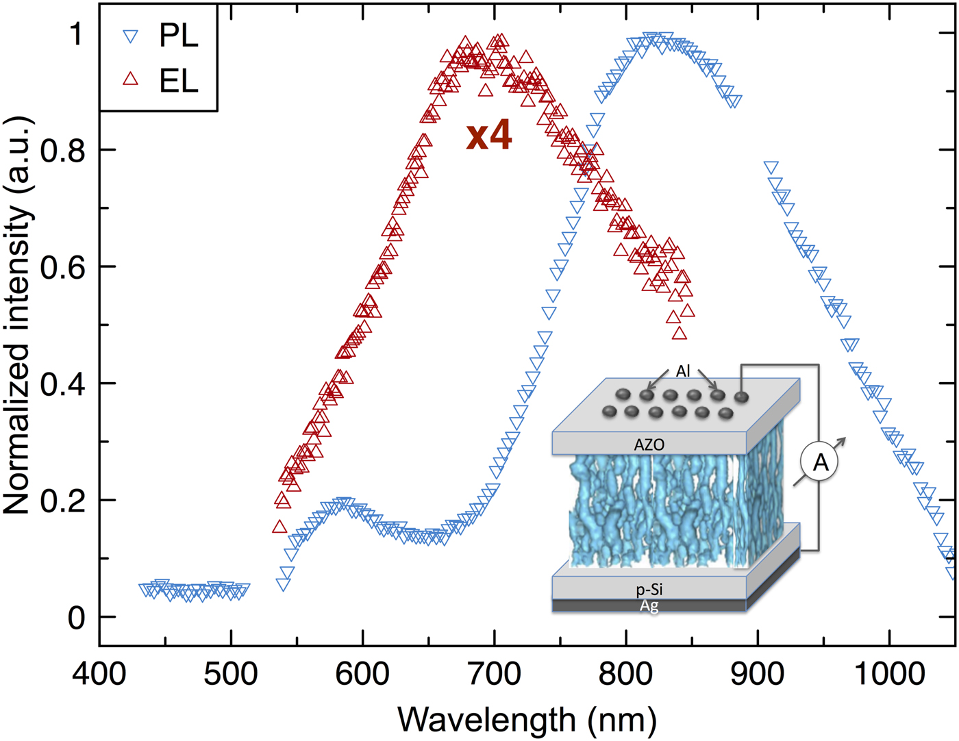
It is also seen from the figure that EL spectra are blueshifted with respect to the PL spectra. Although this shift can stem from a number of phenomena such as selective carrier injection to QDs with different sizes,[Reference Delerue, Lannoo, Allan, Martin, Mihalcescu, Vial, Romestain, Muller and Bsiesy21] impact excitation,[Reference Ossicini, Pavesi and Priolo22] Coulomb blockade,[Reference Abeles, Pinch and Gittleman7, Reference Kastner8, Reference Balberg, Jedrzejewski and Savir11, Reference Nie, Petukhova and Kumacheva18] quantum-confined Stark effect,[Reference Photopoulos and Nassiopoulou23] and enhanced Auger recombination rate at high voltages,[Reference Mihalcescu, Vial, Bsiesy, Muller, Romestain, Martin, Delerue, Lannoo and Allan24] considering the topological information, it is highly likely that Coulomb blockade is the main contributor for the following reasons. First, the selective carrier injection phenomena and quantum-confined Stark effect are generally observed in quantum well structures, and the impact excitation is more likely to occur in well separated Si nanocrystals,[Reference Delerue, Lannoo, Allan, Martin, Mihalcescu, Vial, Romestain, Muller and Bsiesy21, Reference Ossicini, Pavesi and Priolo22] not in a conductive random network such as ours. Second, we observe EL response only with forward bias voltages. However, EL response should be independent of the voltage polarity in the impact excitation model.[Reference Ossicini, Pavesi and Priolo22] Third, as explained above, the current preferably flows through low resistant routes, where the nanowire diameters are larger. This means that, when possible, the narrower passages are avoided, where the possibility of radiative recombination is high. This leads to low EL injection efficiency, and the detection of EL requires a correspondingly high threshold current (~30 V). Last, at high voltages and injection currents, as in our case, the probability of having more than one pair within the same crystallite is possible.[Reference Mihalcescu, Vial, Bsiesy, Muller, Romestain, Martin, Delerue, Lannoo and Allan24] It is known that the Auger recombination dominates over radiative recombination when more than one charge-carrier pair is present within the same nanocrystal.[Reference Mihalcescu, Vial, Bsiesy, Muller, Romestain, Martin, Delerue, Lannoo and Allan24] In a sample with a distribution of crystallite sizes, such as ours, this is expected indeed to cause a blueshift in EL. Therefore, it is highly likely that Auger recombination also contributes to the spectral blueshift. However, as explained above, the three-dimensional (3D) topology of the random network and observed Coulomb gap at low voltages with a non-linear I–V curve strongly suggests that the main contributor is the Coulomb blockade effect.
In conclusion, we have shown that having different microscale and nanoscale topologies has implications for charge transport and photoemission with subtly different characteristics for charges that are locally generated (up to ~10 nm) through the photoelectric effect, and for those that are injected externally through the electrodes (over tens to hundreds of nanometers). We also proved that the optical band gap of this random network could be tuned within a visible light range in a previous study.[Reference Ilday, Ilday, Hübner, Prosa, Martin, Nogay, Kabacelik, Mics, Bonn, Turchinovich, Toffoli, Toffoli, Friedrich, Schmidt, Heinig and Turan3] These suggest that the random network topology can effectively be used in photovoltaic devices with tandem configurations,[Reference Shah25, Reference Pavesi and Turan26] where in each layer a random network with a different band gap can be used, or, in a p–i–n (p-type semiconductor/insulator/n-type semiconductor) junction configuration,[Reference Shah25, Reference Pavesi and Turan26] where a single thin-film layer of a random network can be doped with phosphorus and boron to make n- and p-type layers on thin, bottom, and top portions, respectively. In a p–i–n configuration, charge-carrier pairs are generated in the i-layer, since the light is only absorbed in this wide region. Then, these carriers are separated by the built-in electric field produced in p- and n-type layers.[Reference Shah25, Reference Pavesi and Turan26] This enhances light harvesting owing to the wide i-layer, which also ensures tolerance against high levels of defects and impurities, a technical difficulty faced by conventional p–n junction devices.[Reference Shah25, Reference Pavesi and Turan26] In order for these configurations to work effectively, the Fermi levels of each layer must align on the same height. This is a notoriously difficult problem to overcome;[Reference Shah25, Reference Pavesi and Turan26] however we expect that such concerns will not largely affect random network device configurations since the same material (random network) will be used in all layers.
Supplementary material
The supplementary material for this article can be found at https://doi.org/10.1557/mrc.2017.83.
Acknowledgments
The author thank René Hübner for his contributions to the EFTEM analyses, Ty J. Prosa and Isabelle Martin for their contributions to the APT analyses, and Rasit Turan for providing the use of equipment.


