





Introduction
Radio frequency (RF) superconducting (SRF) cavities, which offer higher accelerating gradients and reduced energy consumption, are increasingly utilized in modern particle accelerators such as the European Spallation Source (ESS), the X-ray Free Electron Laser, the Linac Coherent Light Source-II, and the proposed International Linear Collider. SRF cavities require charging to a specific electric field before beam injection. High-power RF sources, such as Klystrons, tetrodes, inductive output tubes (IOT), and solid-state power amplifiers (SSPAs), are employed to provide the nominal RF power to generate the required electric field. Preliminary results of an experimental demonstration of envelope tracking (ET) techniques applied on a kilowatt level amplifier have been reported with the potential to be scaled up and used to charge SRF cavities [Reference Hoang Duc and Dancila1]. An earlier version of this paper was presented at the Swedish Microwave Days 2023 Conference and was published in its Proceedings [Reference Hoang2].
Conventional charging methods involve a step charging profile to reach the nominal electric field. During the initial filling phase, the cavities act as mismatched load resulting in significant reflected RF power, see Fig. 1 where the theoretical computations illustrate the forward and reflected power profiles for both step charging and optimal charging schemes, as presented in [Reference Bhattacharyya, Ziemann, Ruber and Goryashko3].
The theoretical calculations led to the proposal of a novel strategy for SRF cavity filling, employing a time-varying RF power profile to minimize the total reflected power. The current work introduces and experimentally demonstrates a time-filling profile for the SRF cavities of ESS, demonstrating superior performance compared to the conventional step-charging strategy. The RF power sources required for ESS’ cavities are estimated to be around 400 kW with a 5% duty cycle (3.5 ms pulse width at a repetition rate of 14 Hz).
In the optimal filling scheme, the reflected power starts at a low value of 8 kW compared to 400 kW in step filling and then exponentially decreases as the filling progresses. For ESS spoke cavities [Reference Peggs4], the wasted energy resulting from full power reflection during step filling is estimated to be around 30 MWhrs during long-term operation of approximately 8000 h per year. The wasted energy estimates for medium- and high-beta cavities are even higher at 150 and 550 MWhrs, respectively. Implementing the optimal control scheme during cavity filling becomes crucial for the accelerator design having in mind sustainability and energy efficiency. SSPAs could offer the best performance with the optimal charging scheme, however, their efficiency in the low and medium power range is sub-optimal. Envelope tracking [Reference Asbeck and Popovic5], known as ET, is a suitable solution for maintaining efficiency in the low and mid-power ranges.
Schematic relationship between cavity field and RF driver power using a step filling scheme. During the filling process, the power (indicated by the shaded blue area) is completely reflected due to the impedance mismatch.

This paper showcases the practical implementation at the kilowatt level of the theoretical framework proposed in [Reference Bhattacharyya, Ziemann, Ruber and Goryashko3], while also enabling the potential extrapolation to the nominal power of 400 kW. The optimal charging power profile is implemented without compromising energy efficiency by dynamically modulating the drain voltage. The proof-of-concept utilizes a 352 MHz single-ended SSPA module [Reference Haapala, Eriksson, Hoang Duc and Dancila6] and a commercial modulator (SM52-30), representing the first demonstration of kW-level ET single-ended amplifiers as part of the development of a solid-state-based 400-kW RF power source [Reference Dancila, Rydberg, Eriksson, Goryashko, Haapala, Ruber, Wedberg, Yogi and Ziemann7] for the proton accelerator at ESS.
The paper is organized as follows: section “Optimal charging scheme and conceptual architecture of solid-state based power station” provides a brief introduction to the derivation of the optimal charging scheme based on voltage and current equations inside an ESS SRF cavity. A shaping function tailored to fit the trajectory of the optimal charging scheme of a kilowatt-level single-ended amplifier is described. Section “Architecture of envelope tracking power amplifier and measurement setup” presents insights into the ET system with the shaping function and characterization system. Measurement results of the proposed ET system are presented in section “Measurement results of the ET system”, along with the implementation of a linearization technique. Section “Discussion” discusses the upscaling of power to 400 kW based on the proposed ET module using the optimal charging scheme. A comparison of energy savings from the wall plug between ET technology and other established technologies such as Tetrode and Klystrode is included. Finally, Section “Conclusion” concludes the paper.
Optimal charging scheme and conceptual architecture of solid-state based power station
Optimal charging scheme
A parallel resonant circuit driven by a current generator describes well the evolution of the accelerating field within the cavity, as depicted in Fig. 2.
The block diagram of RF system for powering the cavity (top) and the equivalent circuit with shunt cavity model (bottom).

The beam is modeled as a current source, where the DC beam current is half of the bunched RF current,  $I_{b,RF}$ for short bunches of charged particles. Two common figures of merit are used to characterize the accelerating cavities [Reference Wangler8]. First is the geometric shunt impedance, $R/Q$ of the cavity, defined as follows:
 \begin{equation}
R/Q = \frac{1}{2}\frac{V_c^2}{\omega_0 U_{st}},
\end{equation}
\begin{equation}
R/Q = \frac{1}{2}\frac{V_c^2}{\omega_0 U_{st}},
\end{equation} where Ust represents the energy stored in the cavity, Vc denotes the nominal voltage at which the cavity is excited, and ω 0 is the cavity resonant frequency. The shunt resistance at a specific frequency reflects the efficiency of acceleration per unit of stored energy. The second factor is the well-known quality factor of the bare cavity, unloaded quality factor, Q 0, with the external quality factor, Qext representing the quality factor of the coupling. The loaded quality factor, QL is given by  $Q_L = (Q_0^{-1} + Q_{ext}^{-1})^{-1}$. In the case of SRF cavities, the loaded quality factor is mainly determined by the external quality factor, and thus $Q_L \approx Q_{ext}$. Using [Reference Tuckmantel9], we can derive a first-order differential equation relating the cavity voltage, V(t) to the generator current, $I_g(t)$:
 \begin{equation}
t_F{\dot{V}(t)} + \left( 1-i \frac{2(\omega_0 - \omega)}{\omega}Q_L\right)V(t) = 2Z_L T I_g(t),
\end{equation}
\begin{equation}
t_F{\dot{V}(t)} + \left( 1-i \frac{2(\omega_0 - \omega)}{\omega}Q_L\right)V(t) = 2Z_L T I_g(t),
\end{equation} where  $t_F = 2Q_L/\omega$ represents the filling time, ω is the RF excitation frequency, ω 0 is the cavity resonant frequency, T is the time transit factor, and $Z_L = (R/Q) Q_L$ is the loaded cavity impedance. Additionally, the reflected current over time, $ I_r(t)$ can be calculated as follows:
 \begin{equation}
\begin{aligned}
I_r(t) &= \frac{V(t)}{2(R/Q)T} \left( \frac{1}{Q_{ext}} - \frac{1}{Q_0} + 2i\frac{(\omega_0 - \omega)}{\omega}\right) \\
&- \frac{\dot{V}(t)}{\omega (R/Q)T}.
\end{aligned}
\end{equation}
\begin{equation}
\begin{aligned}
I_r(t) &= \frac{V(t)}{2(R/Q)T} \left( \frac{1}{Q_{ext}} - \frac{1}{Q_0} + 2i\frac{(\omega_0 - \omega)}{\omega}\right) \\
&- \frac{\dot{V}(t)}{\omega (R/Q)T}.
\end{aligned}
\end{equation} The ESS’ spoke cavities are characterized by an external quality factor of  $Q_{ext} = 1.76 \times 10^5$. There are 26 spoke cavities with a geometric beta, $\beta_g = 0.5$ (accelerating velocity related to the speed of light $\beta_g = \frac{\displaystyle \nu}{\displaystyle c}$, each accelerating cavity requiring a peak power of 400 kW and operating at 352 MHz with a transit time factor of T = 1 [Reference Peggs4]. For the step charging scheme, the optimal beam injection time is determined to be $t_i = 0.8t_F\approx 127 \; \mu s$, while the time instant when the reflection is zero is $t_i = 0.69t_F \approx 110 \; \mu s$. The reflection power increases to approximately 3.7 kW and remains constant after beam injection, as shown in Fig. 3 following [Reference Bhattacharyya, Ziemann, Ruber and Goryashko3].
The power profiles of the generator and reflection in two different schemes are shown: the step function (represented by the purple and brown traces) and the optimal function (represented by the red and blue traces). With the optimal charging scheme, the reflection power is significantly reduced, reaching as low as 8 kW at the beginning, whereas the step-filling scheme results in nearly 400 kW of reflected power at the start.

Following Bhattacharyya [Reference Bhattacharyya, Ziemann, Ruber and Goryashko3], a novel strategy was proposed to charge ESS cavities, leading to a significant reduction in total power reflection. The instantaneous power of the generator, Pi is represented as follows:
 \begin{equation}
P_i\left(\frac{t}{t_F}\right) = \frac{V_c^2}{2Z_L} \frac{\exp\left(\frac{2t}{t_F}\right)}{4\sinh^2\left(\frac{t_i}{t_F}\right)} \; t \leq t_i,
\end{equation}
\begin{equation}
P_i\left(\frac{t}{t_F}\right) = \frac{V_c^2}{2Z_L} \frac{\exp\left(\frac{2t}{t_F}\right)}{4\sinh^2\left(\frac{t_i}{t_F}\right)} \; t \leq t_i,
\end{equation} where ti represents the beam injection time in the case of optimal charging. This choice results in an optimal voltage profile within the cavity during the charging time  $t \leq t_i$, given by:
 \begin{equation}
V\left(\frac{t}{t_F}\right) = V_C \frac{\sinh\left(\frac{t}{t_F}\right)}{\sinh\left(\frac{t_i}{t_F}\right)}.
\end{equation}
\begin{equation}
V\left(\frac{t}{t_F}\right) = V_C \frac{\sinh\left(\frac{t}{t_F}\right)}{\sinh\left(\frac{t_i}{t_F}\right)}.
\end{equation} As depicted in Fig. 3, the optimal power at the generator exhibits an exponential increase from approximately 8 to 400 kW, contrasting with the constant 400 kW power in the case of step charging. This optimal charging approach achieves a significant reduction in reflection power, starting at 8 kW and gradually decreasing to 0 at around 300  $\mu s$. Consequently, reaching the nominal voltage takes a longer time compared to the time required for step-charging the cavities. In the optimal filling scheme, the beam injection time is determined to be around $2t_F \approx 310 \; \mu s$. This choice strikes an optimal balance between the required peak power, notable gains in reducing reflection energy, and the overall reduction in total energy demand compared to the step charging method, as presented in [Reference Bhattacharyya, Ziemann, Ruber and Goryashko3]. The optimal filling scheme leads to a substantial decrease of approximately 24% in total energy compared to the step charging method. The subsequent section of the paper delves into the exploration of optimal operational schemes for solid-state-based power amplifiers.
Proof-of-concept design module at kilowatt level with optimal shaping function
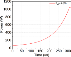
When implementing the optimal filling scheme, each module undergoes the pulse power profile shaping at the kilowatt level, as illustrated in Fig. 4. The input power pulse profile in the time domain is defined, as follows:
The power profile of each module is shown during the first 300  $\mu s$ of a 3.5 ms pulse when utilizing the optimal filling scheme to charge the SRF cavities.
 \begin{equation}
f(t) =
\begin{cases}
K_1 \; 10^{\frac{\frac{10\log_{10}\exp\left({X_{rise}(t) \; K_2}\right)^2}{K_3 \left( \sinh{(2)}^2 \right)}}{20}} & \text{if}\ 0 \leq t \leq 300 \; \mu s, \\
1 & \text{if}\ 300 \; \mu s \leq t \leq 3.5 \; \text{ms}, \\
0 & \text{elsewhere}.
\end{cases}
\end{equation}
\begin{equation}
f(t) =
\begin{cases}
K_1 \; 10^{\frac{\frac{10\log_{10}\exp\left({X_{rise}(t) \; K_2}\right)^2}{K_3 \left( \sinh{(2)}^2 \right)}}{20}} & \text{if}\ 0 \leq t \leq 300 \; \mu s, \\
1 & \text{if}\ 300 \; \mu s \leq t \leq 3.5 \; \text{ms}, \\
0 & \text{elsewhere}.
\end{cases}
\end{equation} The parameters  $K_1, K_2,$ and K 3 in the equation are adjustable. In traditional SSPA, the gain and efficiency are influenced by the bias voltage of the active device and the input drive level [Reference Cripps10]. Our previous work on SSPA [Reference Haapala, Eriksson, Hoang Duc and Dancila6] achieves optimal efficiency in the compression region (kilowatt-level power), which leads to lower operating efficiency at low power and mid-power levels when using the optimal filling function, as shown in Fig. 4.
When considering the optimal filling scheme, it is crucial to examine the total energy demand of the power supply source to realize the improvement in efficiency as compared to the conventional filling scheme [Reference Bhattacharyya, Ziemann, Ruber and Goryashko3]. To achieve the optimal total required energy with the optimal filling approach, it is crucial to maintain high efficiency for each SSPA module across the low-power to high-power range.
In this paper, we propose the application of the ET technique on each SSPA module [Reference Haapala, Eriksson, Hoang Duc and Dancila6] to dynamically adjust the drain voltage based on the input signal function’s envelope, f(t). By selecting appropriate values for  $K_1, K_2,$ and K 3 a shaping function is chosen to operate the module close to its saturation point at every drain voltage. This selection enables an optimal efficiency trajectory, even in the back-off region. In the following section, we demonstrate the implementation of a proof-of-concept ET PA, which could serve as the core of a 400-kW solid-state power source, where many of such amplifiers are linearly combined to the nominal power level.
A 400-kW solid-state power source can be constructed by leveraging previously demonstrated components, such as a Gysel power combiner (detailed in ref. [Reference Jobs, Dancila, Eriksson and Ruber11]), which has been previously utilized to effectively demonstrate a 10-kW power amplifier (detailed in ref. [Reference Dancila, Hoang Duc, Jobs, Holmberg, Hjort, Rydberg and Ruber12]), along with a 12-way high-power combiner (detailed in ref. [Reference Goryashko, Jobs, Hoang Duc, Ericsson and Ruber13]) to reach a 100 kW nominal power. By employing four of these 100 kW amplifiers and integrating them with either a resonant combiner or a hybrid isolated combiner, it is possible to aggregate their output to achieve a combined power output of up to 400 kW.
Architecture of envelope tracking power amplifier and measurement setup
This section presents the design specifics of the ET system, which utilizes the SSPA module described in [Reference Haapala, Eriksson, Hoang Duc and Dancila6], the supply modulator SM52-30, an FPGA-based platform KC705, the Analog-to-Digital Converter (ADC) board (TSW1400), and the Digital to Analog Converter (DAC) board (DAC34SH84EVM).
LDMOS-based power amplifier for ET system
The core component of the proposed ET system is a single-ended LDMOS-based Power Amplifier (PA) that delivers kilowatt-level output power with a drain efficiency of 71%, thoroughly described in [Reference Haapala, Eriksson, Hoang Duc and Dancila6]. The PA module is driven by a broadband linear driver amplifier (ZHL-100W-52+ from Mini-circuits) and operates at a fixed drain voltage (VD) of 50 V. The maximum drain supply voltage for the PA module is also set at 50 V, with a deep class-AB quiescent drain current (ID) of 80 mA. The measurements are conducted using a pulse width of 3.5 ms and a duty cycle of 5%. The gain and drain efficiency characterization of the PA module is performed with an RF pulse signal at 352 MHz, sweeping the PA dynamic range for each drain voltage ranging from 18 to 50 V. The results, depicted in Figs. 5–7, demonstrate that at the maximum output power of 1040 W, the PA module exhibits approximately 19 dB of saturated gain when operated at a drain voltage of 50 V. The phase variation spans from 180 deg to 160 deg. The peak efficiency reaches around 70.4%, but it decreases to 23.3% and 37.4% at 10 and 6 dB output power back-off, respectively.
The gain measured during the pulse (5% duty cycle and a 70 ms period) is plotted as a function of output power for drain voltages ranging from 18 to 50 V. The bold trajectory represents the measurement with fixed 50 V.

The phase measured during the pulse is recorded as a function of output power for drain voltages ranging from 18 to 50 V. The bold trajectory represents the measurement with a fixed 50 V. The compression region is identified above the dashed line.

The drain efficiency measured during the pulse is recorded as a function of output power for drain voltages ranging from 18 to 50 V. The bold trajectory represents the measurement with a fixed 50 V.

Considering the optimal power profile illustrated in Fig. 4, employing the ET system would lead to a significant improvement in drain efficiency, approximately doubling it at 10 dB output power back-off or at the initial stages of the filling time, which happens approximately after 300  $\mu s$ from the start of the filling profile.
Supply modulator for ET system
A supply modulator (SM52-30 from Delta Elektronica) is utilized in the system. This modulator operates at a fixed switching frequency of 200 kHz and offers a high-speed programming option along with a power sink option. These features enable precise control over the rising and falling times, ensuring compliance with the system’s requirements during the first 300  $\mu s$ filling time of the SRF cavity. To achieve an optimal efficiency trajectory, an envelope shaping function is chosen to dynamically adjust the instantaneous DC supply voltage. However, certain shaping functions such as the Wilson shaping function, Nujira N6 shaping function [Reference Cidronali, Giovannelli, Vlasits, Hernaman and Manes14], or adaptive shaping function [Reference Gilabert, Montoro, Ruiz and Garca15] which may introduce nonlinear distortion in the output of the power amplifier, cannot be implemented due to the specifications of the SM52-30 supply modulator.
The SM52-30 power supply could operate in two distinct modes: the fast mode and the saturated mode. In the fast mode, the output capacitance of the supply modulator (SM) is reduced by approximately 10% compared to the normal mode without the high-speed programming option. Specifically, it is about  $91 \; \mu F$. Consequently, it takes approximately $300 \; \mu s$ for the modulator to adjust its output voltage from 17 V to around 42 V, which corresponds to approximately 90% of the desired end voltage when operating with a step control function and a full resistive load. However, increasing the voltage from 42 to 50 V is slower because the modulator’s response follows a capacitor charging trajectory in the saturation mode [Reference Strayer16]. This characteristic introduces non-linear distortion, particularly at high power levels of 1 kW. To address this issue, we propose an approach that combines an envelope-shaping function for the SM52-30 modulator with the pre-distortion of the RF input signal. This approach compensates for the dynamics of the power supply in the saturated mode. The shaping function, denoted as Mopt, not only compensates for distortion but also provides higher efficiency at lower output power levels. A detailed explanation of the shaping function will be presented in the subsequent section.
Architecture of the ET system and measurement setup
The block diagram depicted in Figs. 8 and 9 illustrates the setup of the ET system. The processing board is based on the FPGA Xilinx Kintex-7 (XC7K325T-2FFG900C). This board is connected to a quad-channel 16-bit DAC34SH84EVM, which enables signal generation with an analog bandwidth of up to 100 MHz and facilitates time alignment between the SM path and the RF path. One channel of the DAC is utilized to generate the envelope shaping function for the SM, while the other channel generates the RF pulsed signal. For the DAC board, an external clock signal of 1400 MHz is provided by HM8135. The DAC34SH84EVM board generates an ultra-low jitter clock internally, serving as a reference clock for the FPGA board and the TSW1400 board.
Block diagram of the ET system and measurement setup.

Photograph of FPGA-based platform. The ADC and DAC boards are connected to KC-705 platform via high speed FMC adapter.

In the SM path, the analog output from one channel of the DAC is amplified using a linear amplifier, constructed around a high slew-rate operational amplifier (OPA577). It is important to bypass the RF transformer and a 5th-order low-pass filter at the output because their cut-off frequency exceeds 2 MHz. More details about the shaping function for the SM will be presented in the subsequent section. It should be noted that the capacitors at the drain of the SSPA module must be minimized to enable fast envelope modulation [Reference Hoversten, Schafer, Roberg, Norris, Maksimovic and Popovic17, Reference Florian, Cappello, Niessen, Paganelli, Schafer and Popovic18, Reference Cappello, Florian, Niessen, Paganelli, Schafer and Popovic19].
In the RF path, the signal is initially generated in digital baseband and then digitally up-converted to 352 MHz using a digital up converter (DUC). The resulting pulsed RF signal is subsequently amplified by a driver amplifier before driving the 1 kW SSPA module [Reference Haapala, Eriksson, Hoang Duc and Dancila6].
The output power from the SSPA module is coupled out using a high-power coupler. These reference signals are then attenuated and divided into two paths for feedback and measurements, as depicted in Fig. 8. One of the reference signals undergoes down-conversion, sampling, and analysis in the time domain using a digital oscilloscope (RTO1024). The oscilloscope simultaneously samples the SSPA drain voltage  $V_{dd(t)}$ and current $I_{dd}(t)$ with the help of voltage and current sensors. The software-controlled time alignment ensures synchronization among these signals. A master trigger from the processing board is utilized for synchronization purposes. The calibration details of the measurement setup can be found in [Reference Hoang Duc, Bhattacharyya, Goryasko, Ruber, Rydberg, Olsson and Dancila20].
The feedback signal is subjected to band-pass filtering before being fed into the TSW1400 board. The filtered signal is under-sampled at a maximum rate of 250 MSPS (mega-samples per second). A firmware written in VHDL is loaded onto the KC705 board. This firmware generates digital commands to process the I/Q signal captured by the ADC board, implementing pre-distortion and a proportional-integral (PI) control loop. The pre-distorted IQ signal is then upconverted and fed into the PA driver, ensuring synchronization with the supply voltage to maximize drain efficiency. In this paper, the implementation of the pre-distortion function using look-up tables (LUTs) is carried out at a sampling rate of 10 Msps (mega-samples per second) with an FPGA clock frequency of 125 MHz.
Optimal envelope shaping strategy
The shaping function is designed to optimize efficiency by selecting appropriate values for K 1 and K 2 in the SM path, as well as  $K_1, K_2,$ and K 3 in the RF path. The dynamic power supply system operates in three distinct regions: L-mode, where output power is independent of the supply voltage; P-mode, where output power depends on both supply voltage and input power; and C-mode, where the supply voltage influences the output power [Reference McCune21]. Based on the pulse profile shown in Fig. 4, the operation of the ET system described in this paper falls within the P-mode region at low voltage power supply and the C-mode region at high output power.
As mentioned earlier, the SM is uncontrollable in the saturation mode, leading to high non-linearity in the output response of the PA module when delivering kilowatt-level power. To mitigate this non-linearity in C-mode operation, a pre-distortion technique is employed, as illustrated in Fig. 10. The envelope shaping function is optimized for higher efficiency with values:  $K_1 = 7.75, K_2 = 1, K_3 = 4$, following Equation (6). The processing board ensures time alignment between the RF path and SM path to maximize the efficiency of the ET system. The subsequent section will focus on the characterization of the ET system.
The presented shaping control function illustrates the operation of the drain voltage supply. Around 350 µs, the supply transitions into saturation mode, which corresponds to C-mode operation in the envelope tracking (ET) system.

Additionally, a step function is incorporated in the first  $200 \; \mu s$ to generate a minimum supply voltage of approximately 17 V. For the SM path, the discrete values of the optimized shaping function, $M_{opt} = 0.3815 \; \text{for} -200 \mu s \leq t \leq 0 \; \mu s$, are generated by the processor board and sent to the DAC34SH84EVM. These values are subsequently amplified by a highly linear operational amplifier with a gain of around six times, as depicted in Fig. 10. In the RF path, the function f(t) with $K_1 = 7.75, K_2 = 1.19, K_3 = 4$ is representing the sampling frequency and is up-converted to generate the RF pulsed signal at 352 MHz.
Measurement results of the ET system
In this section, the ET system is characterized and compared to fixed drain bias operation using the optimal charging scheme.
Characterization of the ET system
No additional capacitors are introduced at the drain of the kilowatt-level SSPA module to facilitate the fast supply modulation. The connection between the SM and the SSPA module is minimized to prevent instability arising from low capacitance at the drain terminal. The resistance of the SM causes a voltage drop at the output, resulting in a decrease in the SSPA module’s efficiency. When delivering 1 kW output power at approximately 27 A, the drain voltage experiences a drop of 1.67 V, equivalent to an output resistance of approximately 61.85 mΩ. It should be noted that the output resistance of the SM, as per the SM52-30 datasheet, is around 3.5 mΩ without RF power. To optimize the efficiency and linearity of the ET system, a  $100 \; \mu s$ delay is introduced between the RF path and the supply path. This time alignment plays a crucial role in achieving optimal linearity [Reference Wang, Yang, Kimball, Larson and Asbeck22]. The C-mode operation is observed at approximately 250 $\mu s$, and non-linearity is introduced from 300 $\mu s$ to 420 $\mu s$, as depicted in Fig. 10. To compensate for this non-linearity, a pre-distortion technique is employed. In the P-mode region, the gain of the SSPA module significantly decreases at low drain voltage and input power, as illustrated in Figs. 11 and 12.
The time-domain waveforms of voltage and current are shown, revealing a decrease in drain voltage of approximately 1.67 V. The peak power observed at the flat-top of the pulse is 1 kW.

The waveforms of DC and RF power are presented, demonstrating the utilization of an optimal shaping function to achieve higher efficiency. The non-linearity of the system is visible in the C-mode operating region.

Consequently, the pre-distorter gain is necessary to provide gain expansions from the beginning of the pulse up to around 250  $\mu s$, enabling adherence to the optimal shaping function mentioned in Fig. 4.
Next, the presented ET system undergoes characterization in terms of both the efficiency of the SSPA in combination with the efficiency of the SM. The composite efficiency of the ET system is defined as the product of the efficiency of the SM (ηSM) and the efficiency of the SSPA module when operating under the optimal charging scheme.
The SM is characterized using a power analyser (PCE-830) at a nominal input voltage of 230 Vac [Reference Strayer16]. The input power is computed by the power analyser, while the DC output power is measured using the aforementioned measurement setup. The efficiency is measured to be approximately 92% over a wide range of DC output power, indicating that the composite efficiency is primarily dominated by the efficiency of the SSPA module. A comparison of the SSPA module’s efficiency in cases of using a dynamic power supply and the fixed drain voltage is presented in Fig. 13.
The drain efficiency of the SSPA module is demonstrated at kilowatt output power, both with dynamic drain voltage and with a fixed drain voltage.

At low output power, the efficiency improves by a maximum of 30 percentage points compared to the case without dynamic power supply. The efficiency of the SSPA module at the peak power of 1 kW reaches around 71%. The difference in efficiency between the SSPA module and the ET system is approximately 3.2 percentage points, as the efficiency of the SM is 92%. In the following subsection, the details of linearization will be presented.
Linearization of the ET system
The pre-distorter, employed for the linearization of the SSPA module operating under SM operation, is implemented in an open loop configuration, as shown in Fig. 8. As previously mentioned, the gain response of the SSPA module is affected by the low drain voltage and input power in the P-mode region. This issue can be resolved by adjusting the drain voltage and input power of the pre-distorter. In the C-mode region, the pre-distorter is selected in such a way that the region from 250 to 275  $\mu s$ corresponds to the inverted characteristics of the SSPA module at a fixed supply drain voltage. The region from 275 to 420 $\mu s$ then follows a triangular decay shape, while the remaining region remains constant, as depicted in Fig. 14. The pre-distorted shaping function, denoted as p(t), incorporates modified values of $K_1, K_2,$ and K 3 depending on whether it belongs to the P-mode region or the C-mode region, as illustrated in Fig. 10.
The presented targeted linear ET system illustrates the behavior in both the P-mode and C-mode regions. In the P-mode region, the pre-distorter gain is increased to compensate for the significant drop in power and drain voltage at low levels. In the C-mode region, ranging from 250 to 420 µs, the signal (depicted by the orange-yellow trace) undergoes pre-distortion, enabling the optimization of linearity as indicated by the dashed black trace.

In the proposed implementation, achieving precise time alignment between the RF path and the SM path is crucial to effectively compensate for the non-linearity in the C-mode region. Even when employing the pre-distorter, the impact of time mismatch can still be observed in Fig. 15.
The introduction of time mismatch between the RF and SM paths is demonstrated, considering both scenarios: no delay and optimal delay of 96 µs. It is evident that the time mismatch adversely affects the P-mode region as well.

For our specific design, a delay of approximately 96  $\mu s$ is chosen to achieve optimal performance in terms of linearity. Figure 16 showcases the predistorter’s drain voltage and current characteristics. In the P-mode region, the drain voltage increases from around 18.8 V, while in the C-mode region, it operates at a higher voltage of approximately 43 V. Minor changes are observed in the current waveform within the P-mode region up to 250 $\mu s$. However, a significant change occurs in the C-mode region from 255 $\mu s$ to 420 $\mu s$ when the pre-distorter is implemented, as evident in the current waveform. The measured drop in drain voltage is approximately 0.75 V, indicating that the output impedance at the drain is around 30 mΩ compared to 60 mΩ before the pre-distorter is applied. As mentioned, the non-linearity in the saturation region is improved, as depicted in Fig. 17.
A comparison is made between the drain voltage and current waveforms in the time domain, considering both cases with and without pre-distortion. The minimum drain voltage is selected at approximately 18 V. With pre-distortion, the value of the drain voltage is adjusted higher in the C-mode region of the SM. It is noteworthy that the SSPA consumes a current of 25 A to achieve a 1 kW output power.

For comparison, the DC and RF waveforms in the time domain are presented, considering both cases with and without pre-distortion under SM operation.

Figure 18 showcases an 8% improvement in drain efficiency with the pre-distorter, while at the peak power range, a 4% enhancement in drain efficiency is achieved. Due to the back-off characteristics of the PA module, we adjust the output power to be 15% higher compared to the theoretical curve in the P-mode region, as shown in Fig. 4. This adjustment enables the practical implementation of the optimal charging scheme when utilizing our linearized ET system.
The utilization of the pre-distortion technique leads to a clear enhancement in efficiency in the low-power region.

Discussion
In this section, we examine the practical implications of our conceptual 400-kW solid-state power source, as previously described, when scaling up based on our linearized ET SSPA module to implement the optimal charging scheme [Reference Bhattacharyya, Ziemann, Ruber and Goryashko3]. Henceforth, we will refer to the presented system as an ET system. By scaling the system, we can observe the efficiency characteristics depicted in Fig. 13. As efficiency directly affects the total energy demand, it becomes interesting to compare the performance of our conceptual ET-based power source with other power sources that utilize well-established technologies for powering SRF cavities, including IOTs (or klystrodes) and tetrodes.
To conduct the comparison, we evaluate the energy loss due to the step filling scheme and the optimal filling scheme. Initially, we focus on examining the dynamic efficiency of the power sources when utilizing the optimal charging scheme in the time domain. This comparison is based on the RF sources gradually storing energy in the SRF cavity during the optimal filling time. Figure 19 illustrates that the proposed linearized ET system exhibits superior dynamic efficiency in the low-power range, as it ramps up in power from the beginning of the filling period until approximately 250  $\mu s$. The ET system demonstrates an efficiency improvement of approximately 20 compared to the klystrode-based power source, and around 30% compared to the tetrode-based power source. As the RF power sources reach higher power levels towards the end of the filling period, the efficiency becomes comparable, with both the ET system and the klystrode amplifiers operating at around 73% efficiency. These results highlight that the optimal charging scheme aligns well with the ET system, enabling improved efficiency during operation. In the case of the step charging scheme, the RF power sources are rapidly driven, and thus they are considered to operate at a single operating point. Consequently, the efficiency of all RF power sources remains constant until the beam is injected.
We present the dynamic efficiency characteristic of our conceptual ET system, which illustrates the relationship between efficiency and output power. This analysis is conducted using the ET modules and the optimal charging scheme.

Next, we characterize the energy savings achieved by different filling schemes when applied to RF power sources based on various technologies. A figure-of-merit, denoted as Rwall, is defined as the ratio of energies from the wall plug for the two filling schemes [Reference Bhattacharyya, Ziemann, Ruber and Goryashko3], expressed by the equation provided in the text. This figure-of-merit allows us to theoretically derive the value of Rwall for several technologies, such as tetrode amplifiers, klystrode amplifiers, and the proposed conceptual ET system, which is intended for powering the required 400 kW output of the ESS SRF cavities. For the conceptual ET system, the computed ratio of consumed energies between the two filling schemes is approximately 24%, indicating energy savings, while the klystrode-based system achieves energy savings of around 4% with a beam injection time of approximately 312  $\mu s$. However, the tetrode-based system consumes more energy when utilizing the optimal charging scheme.
The wall plug efficiency,  $R_{wall} = P_{RF}/P_{AC}$ analysis as a function of the SRF cavity injection time is presented in Fig. 20. The comparison among different kinds of RF power sources demonstrates that the proposed ET system applied to SSPA achieves energy savings of more than 24% at the cost of the beam of particles needing to be injected earlier, around 275 $\mu s$. On a system level, considerations regarding the accelerating fields within the cavities and the cryogenic system to cool the cavities to superconducting temperatures over an extended charging period need to be considered. The calculated results of energy savings in the time domain provide valuable insights for selecting the optimal beam injection time, ensuring the best overall efficiency performance while meeting the nominal power requirement of 400 kW during the flat top of the pulse. Therefore, it can be concluded that injecting the beam of particles at 312 $\mu s$ allows for fulfilling the nominal power for the accelerating fields inside the SRF cavities, despite it comes at one or two percent degradation in the energy savings when using the optimal charging scheme.
Time-domain profile of the dynamic efficiency of RF power sources during the filling period. Our linearized ET system demonstrates higher efficiency compared to other power sources in the low-power range, particularly at the beginning of the filling period. Furthermore, our system shows comparable efficiency to other sources in the high-power range, specifically during the flat top of the pulse after the filling period.

Conclusion
We have successfully implemented the optimal charging scheme on our proposed single-ended kilowatt level SSPA with the goal of scaling up in power up to 400 kW to efficiently charge the ESS SRF cavities and significantly reduce the energy wasted due to the excess reflection resulting from the step charging of the SRF cavity. The presented ET technique has been effectively applied to enhance operational efficiency during the filling period, particularly at low and mid-range power levels when the RF power source gradually increases the signal to establish the accelerating fields within the cavities.
During the optimal filling time, the drain efficiency at low and mid-power levels is improved by a factor of 4 compared to the case of using a fixed voltage of 50 V. These results serve as a foundation for scaling up the power to meet the 400 kW requirements of the ESS cavities, which serves as a model for investigating the energy savings achievable with the proposed ET modules. Furthermore, we compare this proposed technology to other well-established technologies such as tetrodes and IOTs for the optimal charging scheme. In the 400 kW system extrapolation based on the proposed kilowatt level ET modules, we observe a 24% improvement in overall plug efficiency compared to a 4% improvement when using IOTs (or klystrodes), considering the optimal beam injection time of 312  $\mu s$, as well as the required accelerating fields and energy consumption for the cryogenic cooling. This feasibility study of the optimal filling scheme demonstrates the potential of solid-state technology, specifically envelope-tracking energy-efficient power amplifiers, to inspire the adoption of these advancements in the next-generation particle accelerators.
Acknowledgements
The authors would like to thank Anirban Bhattacharyya, Tor Lofnes, and Jörgen Olsson for fruitful discussions.
Funding statement
This research was co-funded by the European Spallation Source (ESS) in a bilateral collaboration project with Uppsala University.
Competing interests
The authors report no conflict of interest.

L. Hoang Duc is currently employed as a Power Amplifier Engineer at Ericsson, Long holds a Ph.D. in Microwave Engineering obtained in 2019 from the Department of Engineering Sciences, Solid State Electronics Division at Uppsala University. He also worked as a visiting Ph.D. student at Cardiff University. Long earned a Master of Information, System, and Technology from Université Paris XI, Ha Noi in November 2012.

D. Dancila completed his Ph.D. in Microwave Engineering at the Université catholique de Louvain in 2011, focusing on research related to RF-MEMS and microfabrication technologies for millimeter-wave components, which was conducted at IMEC in Belgium. Since March 2019, he held the position of Associate Professor at Uppsala University, where he currently teaches courses in electronics and microwave engineering. He is heading the microwave group and leads research activities within areas such as millimeter-wave antenna arrays and reflectarrays, RF sensors, and high-power highly efficient RF and microwave amplifiers at the FREIA laboratory. In addition to his academic achievements, he possesses a formal education in Business Management, which he acquired from the Solvay Business School in Brussels. He has also founded the spin-off company Percy Roc AB, with a primary focus on material processing utilizing high-power microwave technology.


 Open access

