




I. INTRODUCTION
Thermoelectricity is a process of direct inter-conversion of thermal and electrical energy using a solid-state engine. The efficiency of a thermoelectric engine is related to a material dependent figure of merit, ZT and the Carnot efficiency. Z is given as α2σ/κ, where α is Seebeck coefficient or thermopower, α2σ is power factor, and σ and κ are electrical and thermal conductivity respectively. Reference Rowe1 Due to conflicting inter-relationships between these three parameters, every material has an optimal Z, and significant fraction of research on thermoelectrics has been focused on identifying high efficiency thermoelectric materials and optimizing their ZT. Reference Rowe1,Reference Snyder and Toberer2 The two key methods for optimizing Z are reduction of lattice or phonon thermal conductivity without affecting the electrical properties, Reference Bhandari and Rowe3 and tuning the carrier concentration (very rarely band structure) by doping or alloying. Reference Rowe, Bhandari and Rowe4 While a thermoelectric engine possesses several advantages over other waste heat recovery technologies, such as lack of moving parts, reliability etc., low efficiency of thermoelectric engines have limited their application for waste heat recovery. Reference Rowe1
Although optimization of thermoelectric properties of known semiconductors have been successful in achieving high Z, further improvements in Z and expanding the operating temperature range of thermoelectric engine requires renewed materials discovery efforts. Reference Snyder and Toberer2,Reference Bell5 One of the paradigms that had dictated the search for high efficiency thermoelectric materials has been the “phonon glass and electron crystal (PGEC)” paradigm proposed by Slack. Reference Slack and Rowe6 Several new materials showing high thermoelectric efficiency were discovered with this mechanism as the basis. Reference Nolas, Cohn, Slack and Schujman7–Reference Nolas, Cohn, Slack and Schujman9 Later, the prediction of high thermoelectric efficiency in low dimensional materials by Dresselhaus Reference Hicks and Dresselhaus10,Reference Hicks and Dresselhaus11 led to experimental realization of several high efficiency nanostructured thermoelectric materials. Reference Harman, Spears and Manfra12–Reference Biswas, He, Blum, Wu, Hogan, Seidman, Dravid and Kanatzidis15 An extensive review of nanostructured thermoelectric materials can be found elsewhere. Reference Vineis, Shakouri and Majumdar16 Most of the materials discussed above are semiconductors, which are composed of heavy elements that are either toxic or not earth abundant. This limits the large scale sustainable deployment of thermoelectric materials, even if they have high efficiency. Reference Gaultois, Sparks, Borg, Seshadri, Bonificio and Clarke17–Reference LeBlanc, Yee, Scullin, Dames and Goodson19
Recently, the discovery of high thermoelectric efficiency in n-type SrTiO3 (Ref. Reference Okuda, Nakanishi, Miyasaka and Tokura20) and Na x CoO2 (Ref. Reference Terasaki, Sasago and Uchinokura21) generated significant interest in oxide thermoelectrics. These discoveries were unexpected, as oxides have defied most of the materials descriptors necessary to achieve high thermoelectric efficiency. Reference Rowe1 To understand the importance of these discoveries, we must first address the origin of the differences between electronic transport properties of complex oxides and conventional thermoelectric semiconductors such as Bi2Te3, PbTe etc. The conduction and valence band of d-band complex oxides are often d-orbital and d-orbital/p-orbital character, respectively (although some complex oxides can possess s-orbital and p-orbital character), whereas conventional semiconductors are often s-orbital and p-orbital character, respectively. Materials containing s-orbital and p-orbital character often tend to be more dispersive, and hence, possess small effective mass, large bandwidth, and high carrier mobility. On the other hand, the small bandwidth and large density of states in d-band complex oxides are a consequence of d-orbital character, which leads to large effective mass and low carrier mobility. The ionic nature of oxides leads to strong electron–phonon coupling, and hence, small electron relaxation time. However, large density of states and high effective mass leads to large thermopower in these oxides even at very high filling. Reference Mukerjee and Moore22 The same factors such as electron interaction and magnetism that leads to low carrier mobility in oxides often result in high thermopower. Reference Koshibae and Maekawa23,Reference Koshibae, Tsutsui and Maekawa24 These insights also signaled the discovery of possibly new mechanisms toward high thermoelectric efficiency. Although the full potential of these new mechanisms are yet to be fully realized, they make complex oxides one of the most competitive thermoelectric materials system, especially for high temperature applications.
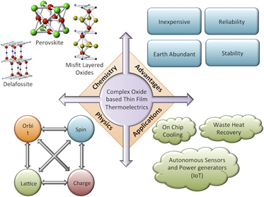
Complex oxides provide a wide range of chemical and structural flexibility to discover high efficiency thermoelectric materials. On the microscopic level, electrons in complex oxides are affected by the interplay between spin, orbital, lattice, and charge degrees of freedom, all of which have profound effects on the thermoelectric properties and offer a completely new approach to thermoelectric research. Additionally, complex oxides are often composed of earth abundant elements, which are inexpensive and environmentally friendly. Thus, they present both scientifically and technologically attractive features for thermoelectric research. These aspects are summarized in Fig. 1. Thin film oxide thermoelectrics provide researchers an efficient platform to access high quality materials (comparable to bulk single crystals) to understand their fundamental transport properties, as bulk single crystal growths are often time consuming and cumbersome. Moreover, with the growing necessity for on-chip cooling in several electronic and photonic technologies, Reference Chowdhury, Prasher, Lofgreen, Chrysler, Narasimhan, Mahajan, Koester, Alley and Venkatasubramanian25 active temperature control in thermochemistry-on-a-chip, DNA microarrays, fiber-optic switches, micro-electro-mechanical systems, Reference Venkatasubramanian, Siivola, Colpitts and O'quinn13 and miniaturized, autonomous, and reliable power generators, and sensors in internet of things (IoT) type applications, Reference Miorandi, Sicari, De Pellegrini and Chlamtac26 thin film thermoelectrics are expected to have an increasing role in applications beyond waste heat recovery and simple cooling applications.
A schematic showing the scientific and technological advantages of complex oxides as thermoelectrics: The bottom left shows how the interplay between different degrees of freedom (spin, charge, lattice, and orbit) enables new possibilities for complex oxide thermoelectrics; the top left shows the structural and chemical diversity, which affects the chemistry of complex oxides and their thermoelectric properties; the top right shows the advantages of complex oxides as materials system for any technological application; the bottom right shows the important applications, where complex oxide thermoelectrics, especially thin films can find an important role.

Several reviews have already addressed the importance of oxide thermoelectrics and some of the salient materials families have been explored in detail. Reference Koumoto, Terasaki and Funahashi27–Reference Lee, Bock, Trolier-Mckinstry and Randall34 Despite growing interest in thin film oxide thermoelectrics, as far as I am aware of, only one study surveys thermoelectric studies on thin films materials in depth, but was limited to two materials systems namely ZnO and Ca3Co4O9. Reference Mele, Mele, Endo, Arisawa, Li and Tsuchiya35 The aim of this review is to bridge the gap in earlier reviews on studies related to low dimensional thermoelectric oxide materials and also, place an emphasis on discussing the physics behind achieving large thermoelectric figure of merit in these materials. Specifically, this review will discuss the recent developments in the study of thermoelectric and thermal transport behavior of complex oxides, synthesized in the form of thin films, heterostructures, and superlattices. As thermal transport in low dimensional materials is an interesting topic with close relevance to thermoelectric applications, special emphasis will be placed on thermal transport studies.
II. MECHANISMS FOR HIGH THERMOELECTRIC EFFICIENCY
As noted earlier, besides the optimization of carrier concentration, two of the common mechanisms used to achieve high thermoelectric efficiency are: (i) reduction in thermal conductivity due to alloying, nanostructuring of materials, and composite formation, Reference Vineis, Shakouri and Majumdar16,Reference Liu, Yan, Chen and Ren36–Reference Dresselhaus, Chen, Tang, Yang, Lee, Wang, Ren, Fleurial and Gogna41 and (ii) band engineering or tailoring the electronic structure to improve the power factor. Reference Heremans, Jovovic, Toberer, Saramat, Kurosaki, Charoenphakdee, Yamanaka and Snyder42–Reference Pei, Wang and Snyder44 Often such techniques are commonly used for semiconductors to achieve high thermoelectric efficiency. In case of oxides, the mechanisms toward high thermoelectric efficiency are often different and varied in nature. We will first review the doping dependence of thermoelectric properties in conventional materials with a brief discussion on the physics behind it, and discuss some of the new physical mechanisms that lead to high thermoelectric efficiency in complex oxides, to put them in context.
A. Review of doping dependence of thermoelectric properties
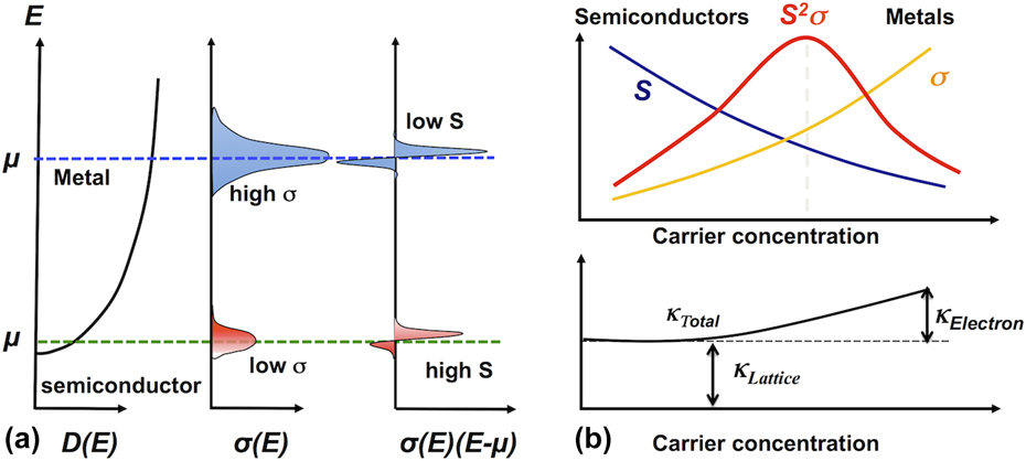
The evolution of the thermoelectric properties as a function of carrier concentration (or equivalently chemical potential) is well understood for conventional materials irrespective of their electrical properties (insulating, semiconducting, semi-metallic, and metallic). These materials follow the conventional band picture of electron transport. Figure 2(a) motivates the physics behind how these properties are derived. Assuming the electron transport in the material is due to a single parabolic band, the density of states scales as square root of energy. Further, as electrons are Fermions, only a small bandwidth of energy (∼few k B T, where k B is Boltzmann constant and T is temperature) close to the chemical potential is relevant for electron transport. As one shifts the chemical potential further into a band from an energy gap, the carrier concentration increases. As one can see, as the chemical potential increases and lies deeper into the band, the differential electrical conductivity (one should integrate the differential conductivity over the whole energy range to obtain the electrical conductivity) increases, explaining why metals are good conductors compared to semiconductors. On the other hand, the first order moment of differential electrical conductivity is directly related to thermopower, hence, this value decreases as the chemical potential moves further deep into the band. This explains the origin of low thermopower of metals as compared to semiconducting materials. This conflicting nature of thermopower and electrical conductivity evolution with carrier concentration is the key reason why carrier concentration is used as an optimization parameter to achieve high Z. We show the conflicting nature of all the thermoelectric properties in Figs. 2(b) and 2(c) by plotting these properties as a function of carrier concentration, including thermal conductivity. As one can see, the electronic component of thermal conductivity can shift the optimal carrier concentration to achieve high ZT further from the optimum achieved for the power factor. Moreover, the phonon or lattice thermal conductivity has an important influence on the absolute value of ZT and not on the carrier concentration dependence. In the following discussion, we will review some of the novel mechanisms that enable high Z in oxide materials, to contrast the phenomenology discussed here for conventional semiconductor thermoelectric materials.
Representation of thermoelectric parameters using band theory: (a) the evolution of density of states, differential electrical conductivity, and first order moment of differential electrical conductivity (x-axis) with energy. This schematic clearly distinguishes the thermoelectric properties of semiconductors and metals. (b) The dependence of thermoelectric properties on the carrier concentration. Neither semiconductors nor metals show high power factor due to too low conductivity and thermopower respectively, but the maximum occurs at intermediate carrier density, which corresponds to heavily doped (alloyed) semiconductors. The bottom panel shows that at high carrier density (metallic limit) the electronic thermal conductivity has an important contribution to the total thermal conductivity. This interplay between the three thermoelectric parameters (electrical and thermal conductivity, and thermopower) gives rise to an optical carrier density, which shows maximum power factor.
B. Orbital degeneracy in noninteracting or weakly interacting materials
It is well known that large degeneracy is desirable for increasing thermopower. Conventional high efficiency thermoelectric materials usually possess large valley degeneracy. Reference Rowe1 Transition metal oxides provide an alternate degeneracy mechanism namely orbital degeneracy. The conduction band of most thermoelectric transition metal oxides (especially perovskites) is dominated by the d-band character. Reference Rao and Raveau45,Reference Tokura and Nagaosa46 This d-band nature is the key reason for large orbital degeneracy in titanates, especially SrTiO3 (STO). The transition metal d-orbitals possess the 5-fold degeneracy, when compared to one and three for s- and p-orbitals respectively. The nature of the degeneracy of transition metal oxides is sensitively dependent on the neighborhood of the transitional metal ions in the unit cell of the oxide. For example, STO crystallizes in the perovskite structure (CaTiO3 type) and the nearest neighbor for the Ti4+ ions are the O2−, which forms octahedra around the Ti4+ ions. This octahedra leads to the crystal field splitting of the degenerate d-orbitals into 3-fold low energy t 2g orbitals and 2-fold high energy e g orbitals. Reference Bethe47–Reference Saha, Sinha and Mookerjee49 The low-lying t 2g orbitals form the conduction band in STO. Besides, the small bandwidth of these bands lead to high effective mass in STO, which is considered desirable to achieve large thermopower, even if it adversely affects mobility. Reference Wunderlich, Ohta and Koumoto50 This is one of the important consequences of the large orbital degeneracy, which enables high thermopower in STO even at very large dopant concentration such as 1021 cm−3. Unfortunately, the low electron mobility of STO at room temperature (and higher temperatures) is largely due to strong electron–phonon coupling, which is the primary limitation for further increasing power factor at room temperatures or higher. Reference Tufte and Chapman51–Reference Mikheev, Himmetoglu, Kajdos, Moetakef, Cain, Van De Walle and Stemmer55 Besides high effective mass, enhanced scattering rates of electrons (e.g., with phonons) is another reason for low mobility in such large density of states materials.
Okuda et al. achieved one of first experimental demonstrations of high thermoelectric power factor in complex oxides by systematically doping STO with La. They showed large thermoelectric power factor [∼36 μW/(cm K2)] in n-type doped STO at room temperature and established that large orbital degeneracy can lead to high power factor. Reference Okuda, Nakanishi, Miyasaka and Tokura20 Such a large thermoelectric power factor is comparable to the state-of-the-art room temperature thermoelectric material, Bi2Te3. Reference Ovsyannikov, Shchennikov, Vorontsov, Manakov, Likhacheva and Kulbachinskii56 Unfortunately, the larger thermal conductivity of STO [∼10 W/(m K)] leads to a ZT of ∼0.1 at room temperature, as compared to Bi2Te3's ZT of ∼1–1.5. Reference Okuda, Nakanishi, Miyasaka and Tokura20,Reference Ovsyannikov, Shchennikov, Vorontsov, Manakov, Likhacheva and Kulbachinskii56 Several strategies to improve the figure of merit by tailoring both the electrical and thermal properties are currently underway. Besides SrTiO3, other oxide materials such as doped SrNb2O6, Reference Lee, Bock, Trolier-Mckinstry and Randall34,Reference Lee, Yang, Wilke, Trolier-Mckinstry and Randall57,Reference Lee, Wilke, Trolier-Mckinstry, Zhang and Randall58 and Ba1−x Sr x PbO3 Reference Yasukawa and Murayama59,Reference Yasukawa and Murayama60 that are being explored for potential high temperature applications.
C. Orbital and spin degeneracy in strongly interacting materials
So far, we discussed electron transport in complex oxides, which can be explained by noninteracting or weakly interacting picture. In most complex oxides, this model fails, due to strong electron–electron correlation. Strong electron correlation (or electron–electron interaction) has been the subject of several interesting articles, Reference Imada, Fujimori and Tokura61,Reference Zaanen, Sawatzky and Allen62 and we will provide a succinct summary of our current understanding of thermoelectric properties in strongly correlated systems. In a noninteracting or weakly interacting picture, one can assume that the kinetic energy of the electrons is much greater than the periodic potential, which the electron experiences due to the presence of ionic lattice. In the strongly correlated regime, the on-site potential due to the lattice is much greater than the kinetic energy of the electrons, and hence, we need a completely different model to understand electronic transport. The electron transport, especially thermoelectric transport, in the strongly correlated regime has been a subject several theoretical investigations and provide a simple framework to explain all transport quantities. Reference Mukerjee and Moore22,Reference Beni63–Reference Chaikin and Beni65 This model, often called the single band Hubbard model, studies the evolution of various transport and physical properties for a strongly correlated system with on-site potential, U and hopping energy or bandwidth, t at a given temperature T. For a given site, to achieve a carrier occupation number other than 1, one has to pay an energy cost of U and the energy cost for a carrier hopping from one site to another is t. For a strongly correlated system, U ≫ t. The thermoelectric transport quantities such as electrical conductivity, thermopower, and electronic component of thermal conductivity etc. can be derived as analytical expressions. Reference Mukerjee and Moore22 The results from such a model can elucidate the evolution of power factor (TS 2σ shown in y-axis) as a function of ρ or filling (average electron or carrier occupation on a site shown in x-axis) in Na x CoO2, which is one of the important correlated thermoelectric oxide [shown in Fig. 3(a)]. Many correlated perovskite oxides such as manganites [especially CaMnO3 (Ref. Reference Ohtaki, Koga, Tokunaga, Eguchi and Arai66−Reference Hébert, Martin, Maignan, Frésard, Hejtmanek and Raveau68)], chromates, Reference Weber, Griffin and Bates69 ruthanates, Reference Hebert, Klein, Maignan, Hejtmanek and Dabrowski70 and cobaltates Reference Terasaki, Sasago and Uchinokura21,Reference Funahashi, Matsubara, Ikuta, Takeuchi, Mizutani and Sodeoka71–Reference Lee, Viciu, Li, Wang, Foo, Watauchi, Pascal, Cava and Ong73 show promising thermoelectric properties and largely follow this formalism.
(a) Doping dependence of thermoelectric power factor in Na x CoO2. The material is a band insulator for ρ = 0.2, and a Mott insulator for ρ = 1. The maximum obtained at ρ = 0.88 agrees well with experimental results. Reprinted from Ref. Reference Mukerjee and Moore22 with the permission of AIP Publishing. (b) The calculated total degeneracy (spin + orbital) for cobaltates depending on their valence and spin configurations. The electronic configuration is shown for each case. Reprinted figure with permission from Ref. Reference Koshibae, Tsutsui and Maekawa24. Copyright (2000) by the American Physical Society.
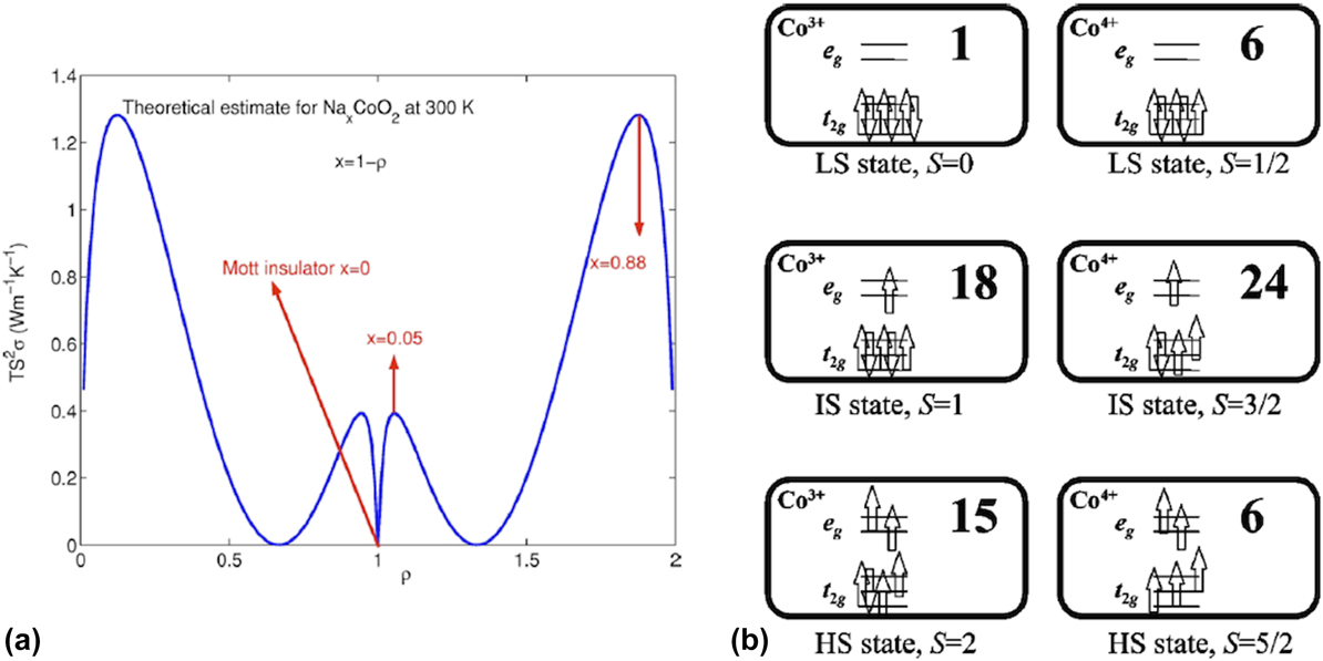
Among these compounds, cobaltates show very high figure merit over a wide temperature range, Reference Funahashi, Matsubara, Ikuta, Takeuchi, Mizutani and Sodeoka71,Reference Lee, Viciu, Li, Wang, Foo, Watauchi, Pascal, Cava and Ong73 and is considered one of the most important high temperature thermoelectric systems, especially for p-type oxides. Reference Hébert, Berthebaud, Daou, Bréard, Pelloquin, Guilmeau, Gascoin, Lebedev and Maignan74,Reference Sootsman, Chung and Kanatzidis75 The large thermoelectric power factor observed in cobaltates is explained using spin degeneracy. Reference Koshibae and Maekawa23,Reference Koshibae, Tsutsui and Maekawa24 Later, this hypothesis was verified experimentally using in depth transport studies. Reference Wang, Rogado, Cava and Ong76 For cobaltates, the valence state ranges from +3 to +4 with 6 and 5 electrons to be filled in the d-bands. Ideally, one would expect the low spin state (t 2g Reference Slack and Rowe6 for Co3+ and t 2g Reference Bell5 for Co4+) to be stable, but the competition between the crystal field splitting energy and the Hund's rule coupling (intra-atomic exchange) can help us access states with larger degeneracy, which is often dubbed as spin degeneracy. This competition is also responsible for partially filled t 2g and e g orbitals, and degenerate spin states in cobaltates (low spin: t 2g 6 for Co3+ and t 2g 5 for Co4+, intermediate spin: t 2g 5 e g 1 for Co3+ and t 2g 4 e g 1 for Co4+ and high spin: t 2g 4 e g 2 for Co3+ and t 2g 3 e g 2 for Co4+). This spin degeneracy, on top of the orbital degeneracy possible in these systems, gives rise to large thermoelectric power in cobaltates [the electronic structures and the degeneracies are schematically shown in Fig. 3(b)]. The combined effect of spin and orbital degeneracy leads to large thermopower only in triangularly coordinated cobalt lattices as seen in Na x CoO2, where the bond angle for Co–O–Co bonds is 90°. Reference Koshibae, Tsutsui and Maekawa24 This framework can also be used to understand the thermally induced spin transition that happens in perovskite cobaltates. Reference Goodenough77 Further, the layered structure of these cobaltates leads to very low thermal conductivity, Reference Terasaki, Tanaka, Satake, Okada and Fujii78 as they follow the nanostructured block layered concept. Reference Fujii, Terasaki, Kanatzidis, Mahanti and Hogan79 Thus, cobaltates have emerged as one of the important high efficiency p-type thermoelectric materials for high temperature applications.
III. SYNTHESIS AND CHARACTERIZATION OF THERMOELECTRIC COMPLEX OXIDE THIN FILMS, HETEROSTRUCTURES, AND SUPERLATTICES
The synthesis of thin films and other low dimensional structures of complex oxides have been an important subject of investigation ever since the discovery of high-T c cuprates. Several thin film growth techniques such as molecular beam epitaxy, Reference Schlom, Eckstein, Hellman, Streiffer, Harris, Beasley, Bravman, Geballe, Webb, Von Dessonneck and Turner80–Reference Eckstein and Bozovic83 pulsed laser deposition, Reference Dijkkamp, Venkatesan, Wu, Shaheen, Jisrawi, Min-Lee, McLean and Croft84–Reference Rijnders, Koster, Leca, Blank and Rogalla86 sputtering, Reference Poppe, Schubert, Arons, Evers, Freiburg, Reichert, Schmidt, Sybertz and Urban87–Reference Sandstrom, Gallagher, Dinger, Koch, Laibowitz, Kleinsasser, Gambino, Bumble and Chisholm93 metal–organic chemical vapor deposition, Reference Bai, Tsu, Wang, Foster, Murray and Dravid94–Reference Kwak, Boyd and Erbil98 and chemical solution deposition Reference Schwartz99 etc. have been used to synthesize high quality complex oxide thin films. As complex oxides have been of interest for a variety of applications, and physical phenomena, a range of synthesis techniques beyond what is discussed above could have been used. In this section, we will discuss some select synthesis and characterization investigations carried out on thin films of thermoelectric complex oxides.
A. Titanates
One of the widely studied complex oxides for thermoelectric applications is the titanate family. STO is a prototypical titanate, which shows large thermoelectric power factor over a wide range of temperatures. Reference Okuda, Nakanishi, Miyasaka and Tokura20,Reference Ohta, Nomura, Ohta, Hirano, Hosono and Koumoto100–Reference Ohta, Nomura, Ohta and Koumoto102 Besides STO, other titanates such as CaTiO3, Reference Bak, Nowotny, Sorrell, Zhou and Vance103,Reference Bak, Burg, Nowotny and Blennerhassett104 and BaTiO3 Reference Brahmecha105–Reference Kolodiazhnyi, Petric, Niewczas, Bridges, Safa-Sefat and Greedan107 were also investigated for their thermoelectric properties. Apart from these studies on typical thin films, thermoelectric properties of other exotic low dimensional structures such as quantum wells, superlattices etc. Reference Ohta, Kim, Mune, Mizoguchi, Nomura, Ohta, Nomura, Nakanishi, Ikuhara, Hirano, Hosono and Koumoto108–Reference Kerman, Ramanathan, Baniecki, Ishii, Kotaka, Aso, Kurihara, Schafranek and Vailionis113 were also studied. After the discovery of large thermoelectric power factor in La doped STO, Reference Okuda, Nakanishi, Miyasaka and Tokura20 several thin film oriented investigations were performed on doped STO using pulsed laser deposition method. As doped STO remains the best n-type oxide thermoelectric material, several in-depth investigations studied the effect of single dopant, Reference Ohta, Nomura, Ohta, Hirano, Hosono and Koumoto100 multiple dopants, Reference Ravichandran, Siemons, Oh, Kardel, Chari, Heijmerikx, Scullin, Majumdar, Ramesh and Cahill101,Reference Abutaha, Sarath Kumar, Mehdizadeh Dehkordi, Tritt and Alshareef114,Reference Kumar, Barasheed and Alshareef115 and their Ruddlesden–Popper phases Reference Lee, Ishizaki, Kim, Ohta and Koumoto116 on the thermoelectric properties of STO based thin films. Interestingly, the very first exploration of thermoelectric properties of heavily Nb doped ternary phase diagram of CaTiO3–SrTiO3–BaTiO3 was carried out using pulsed laser deposition. Reference Yamamoto, Ohta and Koumoto117 Other growth techniques such as sputtering, Reference Baniecki, Ishii, Aso, Kobayashi, Kurihara, Yamanaka, Vailionis and Schafranek118 and molecular beam epitaxy (MBE) Reference Jalan and Stemmer119 were successfully used to grow doped STO films. Especially, MBE grown films demonstrated large cryogenic thermopower due to the phonon drag effect, Reference Cain, Kajdos and Stemmer120 due to exquisite stoichiometry control. The thermal properties of undoped STO were studied using a variety of growth methods to verify the ability of each technique in producing high quality STO films. Reference Oh, Ravichandran, Liang, Siemons, Jalan, Brooks, Huijben, Schlom, Stemmer, Martin, Majumdar, Ramesh and Cahill121,Reference Wiedigen, Kramer, Feuchter, Knorr, Nee, Hoffmann, Kamlah, Volkert and Jooss122
Thin film growth of titanates is a matured research area due to the persistent interest in titanates for ferroelectric applications, especially Ba1−x Sr x TiO3. Several single crystalline substrates are available for the growth of titanates such as CaTiO3 (a pc = 3.826 Å) (a pc refers to pseudocubic lattice parameter, which is an approximate cubic lattice parameter derived for orthorhombic unit cells), SrTiO3 (a = 3.905 Å), BaTiO3 (a = 3.992 Å), and their alloys. Fortunately, SrTiO3 is the widely used perovskite substrate, which is also a common substrate for several thermoelectric complex oxides. Besides STO, other single crystalline substrates such as LaAlO3 (a = 3.79 Å), (LaAlO3)0.3(Sr2TaAlO6)0.7 (LSAT) (a = 3.868 Å), NdGaO3 (a pc = 3.863 Å), DyScO3 (a pc = 3.947 Å), GdScO3 (a pc = 3.961 Å) etc. are widely used to cover the entire range of in-plane lattice parameters possible for the titanate thin film family. The epitaxial relationship between the titanates especially STO and various perovskite substrates can be often simplified as a cube-on-cube geometry. Reference Schlom, Chen, Pan, Schmehl and Zurbuchen123 Despite this advantage, the titanates are prone to be highly nonstoichiometric Reference Brooks, Kourkoutis, Heeg, Schubert, Muller and Schlom124 with profound effect on this physical properties, Reference Oh, Ravichandran, Liang, Siemons, Jalan, Brooks, Huijben, Schlom, Stemmer, Martin, Majumdar, Ramesh and Cahill121,Reference Breckenfeld, Wilson, Karthik, Damodaran, Cahill and Martin125 especially thermoelectric properties. Reference Ravichandran, Siemons, Oh, Kardel, Chari, Heijmerikx, Scullin, Majumdar, Ramesh and Cahill101,Reference Choi, Yoo and Ohta126 For example, in the case of STO, due to the presence of deep valence bands with respect to the vacuum level, only n-type doping is thermodynamically feasible. Reference Robertson and Clark127 Trivalent ions such as La, Pr on the A-site (Sr), pentavalent ions such as Nb on the B-site (Ti), oxygen vacancies, or a combination of these were used as common dopants to achieve n-type conduction in STO. Reference Ohta, Nomura, Ohta, Hirano, Hosono and Koumoto100,Reference Ravichandran, Siemons, Oh, Kardel, Chari, Heijmerikx, Scullin, Majumdar, Ramesh and Cahill101,Reference Abutaha, Sarath Kumar, Mehdizadeh Dehkordi, Tritt and Alshareef114,Reference Baniecki, Ishii, Aso, Kobayashi, Kurihara, Yamanaka, Vailionis and Schafranek118–Reference Cain, Kajdos and Stemmer120,Reference Choi, Yoo and Ohta126 On the other hand, cationic vacancies can act as compensating defects. Reference Ertekin, Srinivasan, Ravichandran, Rossen, Siemons, Majumdar, Ramesh and Grossman128–Reference Janotti, Varley, Choi and Van De Walle130 Hence, understanding the effect of various point defects on the thermoelectric properties of such titanates has been an important issue. Often, it is difficult to elucidate how these defects are created, whether it is dictated by the growth process, thermodynamics, or if they arise from extrinsic causes such as doping/alloying, and other impurities. On top of these challenges, the lack of powerful analytical technique(s) to quantitatively characterize the point defect density and distribution hampers the understanding the interrelationship between point defects and physical properties. Hence, researchers often resort to a combination of techniques to elucidate the nature of point defects in these thermoelectric materials.
Some of the common structural characterization techniques used are x-ray diffraction (XRD), electron microscopy, Reference Brooks, Kourkoutis, Heeg, Schubert, Muller and Schlom124 Rutherford backscattering, Reference Breckenfeld, Wilson, Karthik, Damodaran, Cahill and Martin125 ellipsometry, Reference Choi, Yoo and Ohta126,Reference Sarath Kumar, Abutaha, Hedhili and Alshareef131 etc. XRD remains the most powerful technique to characterize the bulk structural properties of thin films. This method has been widely used to study titanate thin films; especially STO based thin film materials. Figure 4 shows the typical x-ray diffraction based characterization measurements performed on STO based thin films, which include typical Bragg scans (θ–2θ scan), rocking curves, ϕ-scan, and reciprocal space mapping. One can see that the effect of most doping schemes and/or nonstoichiometry is the expansion of the c-axis lattice parameter. The nonselectivity of this lattice expansion has been a subject of several investigations, and hence, limits to use of XRD to quantify the presence of different point defects in STO. Figure 5 summarizes other common characterization techniques such as high resolution scanning transmission electron microscopy, atomic force microscopy, Rutherford backscattering, and optical reflectivity to characterize STO based thin films. Often, a combination of both the structural, chemical probes along with physical property measurements have been more successful in providing some insights into the effect of defects on the thermal and thermoelectric properties. Reference Ravichandran, Siemons, Oh, Kardel, Chari, Heijmerikx, Scullin, Majumdar, Ramesh and Cahill101,Reference Breckenfeld, Wilson, Karthik, Damodaran, Cahill and Martin125,Reference Choi, Yoo and Ohta126,Reference Sarath Kumar, Abutaha, Hedhili and Alshareef131 Other important factors affecting the thermoelectric properties include residual strain and defects created during strain relaxation, often via creation of dislocations.
(A) The evolution of 002 film peak for different La doping of “double doped” STO in a θ–2θ scan; the inset shows the rocking curve for the film and substrate. Reprinted figure with permission from Ref. Reference Ravichandran, Siemons, Oh, Kardel, Chari, Heijmerikx, Scullin, Majumdar, Ramesh and Cahill101. Copyright (2010) by the American Physical Society. (B) The (left) θ–2θ scan and (right) ϕ scans for STO thin films on LAO with various dopants (Pr, La, La & Nb, and Pr & Nb). Reproduced from Ref. Reference Abutaha, Sarath Kumar, Mehdizadeh Dehkordi, Tritt and Alshareef114 with permission of The Royal Society of Chemistry. (C) The evolution of 002 film peak for different growth pressures for “double doped” STO with fixed La doping in a θ–2θ scan. Reproduced from Ref. Reference Choi, Yoo and Ohta126 with permission of Wiley Materials. (D) The reciprocal space map for 1 at% La doped STO film on LSAT substrate. Reprinted from Ref. Reference Baniecki, Ishii, Aso, Kobayashi, Kurihara, Yamanaka, Vailionis and Schafranek118 with the permission of AIP Publishing. (E) The reciprocal space map for various alloy compositions of Nb doped CaTiO3–SrTiO3–BaTiO3 system. Reprinted from Ref. Reference Yamamoto, Ohta and Koumoto117 with the permission of AIP Publishing.

(A) Scanning transmission electron micrograph of STO thin films with different stoichiometries [(a and b) strontium deficient, (c) stoichiometric, (d and e) strontium excess]. Reprinted from Ref. Reference Brooks, Kourkoutis, Heeg, Schubert, Muller and Schlom124 with the permission of AIP Publishing. (B) Rutherford backscattering spectra for STO thin films with different levels of (non)stoichiometry. Reprinted with permission from Ref. Reference Breckenfeld, Wilson, Karthik, Damodaran, Cahill and Martin125. Copyright (2012) American Chemical Society. (C) Atomic force micrograph and (inset) typical reflection high energy electron diffraction pattern for the (Ca, Sr, Ba)Ti0.8Nb0.2O3 thin films. Reprinted from Ref. Reference Yamamoto, Ohta and Koumoto117 with the permission of AIP Publishing. (D) The optical reflectivity curves for “double doped” STO with fixed La doping. Reproduced from Ref. Reference Choi, Yoo and Ohta126 with permission of Wiley Materials.

B. Cobaltates
Misfit layered cobaltates have a general structure consisting of CdI2-type CoO2 layers sandwiched between rock-salt layers or in other cases, ions such as Li, Na etc. The prototypical member of this family is Na x CoO2, which showed large thermoelectric power Reference Terasaki, Sasago and Uchinokura21 and created interest in the family of compounds. The epitaxy of cobaltates is a lot more challenging than titanates, due to their complicated crystal structure. Simpler compounds such as Na x CoO2 have been more successful in achieving some form of in-plane epitaxial relationship with different single crystalline substrates. Synthesis of Na x CoO2 thin films was carried out primarily using pulsed laser deposition, but other methods such as topotactic exchange, chemical solution deposition. Reference Krockenberger, Fritsch, Cristiani, Matveev, Alff, Habermeier and Keimer132–Reference Buršík, Soroka, Knížek, Hirschner, Levinský and Hejtmánek139 Several attempts resulted in epitaxial growth of Na x CoO2, on c-plane sapphire, SrTiO3, SrLaGaO4 etc. Reference Krockenberger, Fritsch, Cristiani, Matveev, Alff, Habermeier and Keimer132,Reference Yu, Gu, Wang, Zhang and Habermeier133,Reference Son, Kim and Cho137,Reference Venimadhav, Soukiassian, Tenne, Li, Xi, Schlom, Arroyave, Liu, Sun, Pan, Lee and Ong140 As sodium in these compounds is a reactive species, these films often suffered from poor stability. These stability issues were addressed using barrier or capping layers and the thermoelectric properties at room temperature were found to be largely stable and comparable to bulk single crystals. Reference Brinks, Heijmerikx, Hendriks, Rijnders and Huijben135
The thin film studies also focused on other notable layered cobaltates such as Ca3Co4O9, Bi2Sr2Co2O y etc. We will not focus our discussions on Ca3Co4O9, as this material has received considerable attention in a recent review article, Reference Mele, Mele, Endo, Arisawa, Li and Tsuchiya35 but we will discuss the growth efforts on Bi2Sr2Co2O y and related compounds. Reference Wang, Venimadhav, Guo, Chen, Li, Soukiassian, Schlom, Katz, Pan, Wong-Ng, Vaudin and Xi141–Reference Zhu, Shi, Dou, Sun, Li, Wang, Li, Yeoh, Zheng and Chen150 The common techniques used for the growth of cobaltates were pulsed laser deposition, chemical solution deposition, and RF sputtering. Figure 6 documents some of the x-ray (θ–2θ scans and ϕ-scans) and microscopic analyses performed on thin films of cobaltates. As one can see, perfect in-plane epitaxial relationship between the film and substrate was hard to achieve, due to the anisotropic and complicated crystal structure of Bi2Sr2Co2O y unlike in Na x CoO2, where epitaxial growth was achieved. Also, film–substrate interface of Bi2Sr2Co2O y contained an amorphous layer, even though this didn't affect the out-of-plane texturing and crystallinity of the films far from the interface.
(A) (Top panel) XRD pattern and ϕ-scan for β-Na x CoO2 thin films. (Bottom panel) XRD pattern and ϕ-scan for γ-Na x CoO2 thin films. Reprinted from Ref. Reference Son, Kim and Cho137 with the permission of AIP Publishing. (B) XRD pattern, pole figure scan, and rocking curve (inset) for Bi2Sr2Co2O y films on YSZ substrate. Reprinted figure with permission from Ref. Reference Ravichandran, Yadav, Siemons, McGuire, Wu, Vailionis, Majumdar and Ramesh143. Copyright (2012) by the American Physical Society. (C) TEM images of Bi2Sr2Co2O y films grown on (a) STO (001), (b) STO (110), and (c) STO (111). Reprinted from Ref. Reference Zhu, Shi, Dou, Sun, Li, Wang, Li, Yeoh, Zheng and Chen150, with permission from Elsevier.

C. Other materials
Apart from titanates and cobaltates, the thin film studies on other materials have been rather limited. Even though thermopower is widely used as an important transport quantity, many transport studies were not primarily focused on thermoelectric properties. Hence, such studies are not reviewed in this article. Although doped CaMnO3 Reference Ohtaki, Koga, Tokunaga, Eguchi and Arai66–Reference Hébert, Martin, Maignan, Frésard, Hejtmanek and Raveau68 is considered one of the important thermoelectric materials, there are few reports of thin film synthesis. Reference Weidenkaff, Robert, Aguirre, Bocher, Lippert and Canulescu151,Reference Alfaruq, Otal, Aguirre, Populoh and Weidenkaff152 Interestingly, the idea of electron filtering to improve thermoelectric properties of superlattices was studied in the model system La0.67Sr0.33MnO3/LaMnO3. Reference Jha, Sands, Cassels, Jackson, Favaloro, Kirk, Zide, Xu and Shakouri153,Reference Jha, Sands, Jackson, Bomberger, Favaloro, Hodson, Zide, Xu and Shakouri154 Other materials studied include p-type conducting CaAlO2, Reference Banerjee, Maity, Ghosh and Chattopadhyay155 LaCo1−x Ni x O3. Reference Robert, Aguirre, Bocher, Trottmann, Heiroth, Lippert, Döbeli and Weidenkaff156
IV. THERMOELECTRIC AND THERMAL TRANSPORT STUDIES
Thin film synthesis of oxide materials is a matured area of research, but the thermoelectric measurements on these thin films present unique challenges. Recent developments Reference Cahill157–Reference Boffoué, Jacquot, Dauscher, Lenoir and Stölzer163 in the thermoelectric metrology for thin films have played a critical role in enabling the studies detailed below.
A. Thermoelectric properties
The thermoelectric properties of thin film materials, especially that of titanates and cobaltates have been reported extensively. As discussed earlier, these investigations were concentrated on these materials exclusively, with few reports on other promising thermoelectric materials. Hence, this section will summarize thermoelectric transport measurement efforts on titanates and cobaltates.
As discussed earlier, doped SrTiO3 is one of the best n-type conducting oxide thermoelectric materials. Large effective mass in STO leads to high thermopower even in very large carrier densities (>1021 cm−3), and hence, a large power factor. Reference Ravichandran, Siemons, Scullin, Mukerjee, Huijben, Moore, Majumdar and Ramesh164 We will discuss some select investigations on doped STO, where extensive temperature dependent thermoelectric properties were reported. Ohta et al. performed one of the first investigations on the thermoelectric properties of Nb doped STO films. Reference Ohta, Nomura, Ohta, Hirano, Hosono and Koumoto100 Due to the solubility limitation of Nb on the B-site of STO, they used the thin film approach to stabilize a large Nb concentration of up to ∼40%. Although the study reported electrical conductivity, thermopower, Hall mobility, and carrier concentration, they estimated the thermal conductivity to be ∼3 W/(m K). Thermal conductivity measurements in thin films of oxide materials are rather challenging, and we will discuss this aspect in more detail in Sec. IV. B. The highest ZT of 0.37 was achieved at 1000 K for the 20% Nb doped STO (SrTi0.8Nb0.2O3) and remains one of the highest ZT achieved in thin film form of STO. Ravichandran et al. reported the first comprehensive study of thermoelectric properties of thin films of doped STO, including thermal conductivity measurements. They used two dopants to explore the effect of both La on the A site, and the oxygen vacancies on thermoelectric properties, as typical single dopants were insufficient to achieve further enhancement of ZT. Oxygen vacancies were incorporated in the La doped STO films by growing the films in varying amount of oxygen partial pressure. These were called as “double doped STO” and idea of using two dopants was to explore the possibility of band engineering in STO, beyond just the tuning of carrier density. Reference Ravichandran, Siemons, Heijmerikx, Huijben, Majumdar and Ramesh165 As the growth at low pressures can lead to other cationic vacancies such as Sr vacancies, Reference Choi, Yoo and Ohta126,Reference Ertekin, Srinivasan, Ravichandran, Rossen, Siemons, Majumdar, Ramesh and Grossman128 it is unclear whether the intended oxygen vacancies were the only type of defects achieved using this procedure. As Sr vacancies act as acceptors, they can act as competing defects in these films. This approach failed to produce any significant enhancement in the power factor, but significant reduction in thermal conductivity, especially at room temperature was observed. The room temperature ZT increased to 0.18 for 5% La doped STO (La0.05Sr0.95TiO3−δ), compared to the earlier reported value of 0.1 in single crystals. Reference Okuda, Nakanishi, Miyasaka and Tokura20 The highest ZT reported was 0.28 at 873 K. One of the important features of this study was the direct thermal conductivity measurements on the films using the TDTR method, to accurately deduce ZT for the films. Reference Cahill157 The summary of the reported thermoelectric properties (electrical and thermal conductivity, thermopower, power factor and ZT) in this study is shown in Fig. 7. Similar study on the effect of La/Nb dopants along with oxygen vacancies was performed by Sarath Kumar et al., who used O2/Ar mixture to control the oxygen vacancy content in the films. Reference Kumar, Barasheed and Alshareef115 They estimated the highest ZT of 0.29 at 1000 K, as they did not report thermal conductivity values at 1000 K. Abutaha et al. extended this double doping idea through a mechanism of doping on both the A- and B-sites of STO (La/Pr on A-site and Nb on the B-site), demonstrating enhancement in thermoelectric properties for double doped samples as compared to samples with single dopant. Interestingly, the temperature dependence of power factor in this study showed a peak at ∼600–700 K, instead of the decreasing trend observed by Ravichandran et al. Reference Ravichandran, Siemons, Oh, Kardel, Chari, Heijmerikx, Scullin, Majumdar, Ramesh and Cahill101 All the thermoelectric properties except thermal conductivity were reported over a wide temperature range of 300–1000 K. The highest ZT reported in this study was 0.016 at room temperature, as the power factor of these films was an order magnitude lower than the highest power factor values achieved in STO. Lee et al. reported the effect of Nb doping on the thermoelectric properties of the Ruddlesden–Popper (RP) phase of STO, Sr2TiO4. Despite the possibility of lower thermal conductivity in RP phases, their power factor was lower than equivalently doped STO films. All the investigations were performed using pulsed laser deposition as the growth technique. All these studies used LaAlO3 (LAO) substrate (lattice mismatch of ∼3% with STO) except Ravichandran et al., who used LSAT substrates with a lower lattice mismatch with STO (<1%). Jalan et al. reported the first study on thermoelectric properties of MBE grown doped STO films. Reference Jalan and Stemmer119 Although no thermal conductivity values were reported, this study achieved the highest power factor of 39 μW/(m K2) achieved in any form of doped STO at room temperature. Cain et al. was able to use the similar growth method to achieve very large cryogenic power factor of 470 μW/(m K2), especially due to the realization of phonon drag effect. Reference Cain, Kajdos and Stemmer120
Thermoelectric properties of “double doped” STO films. (A) Electrical resistivity, (B) thermopower, (C) thermal conductivity, and derived (D) power factor, and (E) ZT for “double doped” STO films over a temperature range of 300–900 K. (F) The evolution of thermopower with carrier density at room temperature and its comparison with the reported values in the literature. Reprinted figure with permission from Ref. Reference Ravichandran, Siemons, Oh, Kardel, Chari, Heijmerikx, Scullin, Majumdar, Ramesh and Cahill101. Copyright (2010) by the American Physical Society.

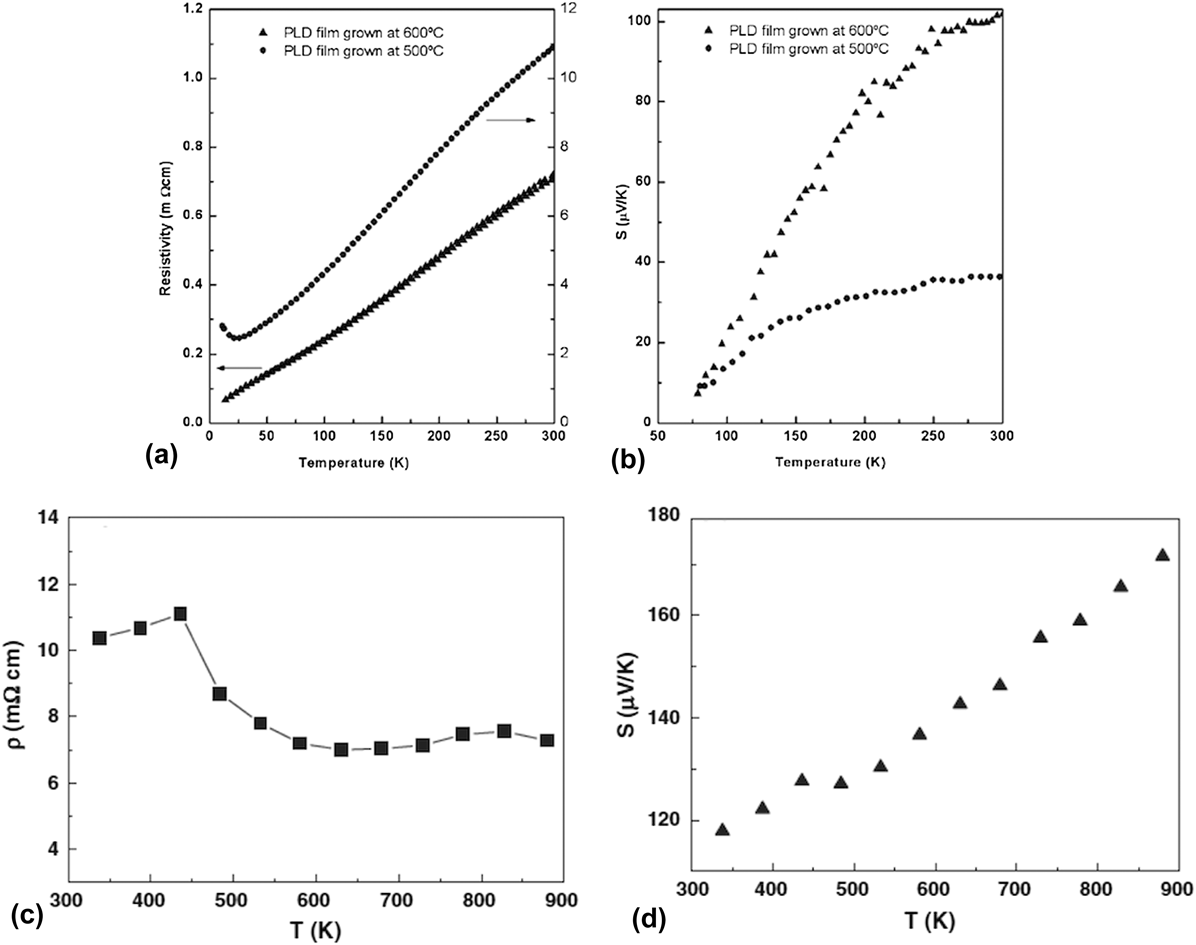
The second materials family is the layered cobaltate family, which is the best p-type conducting oxide thermoelectric materials system. There are few reviews, which cover some aspects of this materials system, such as Ca3Co4O9 thin films, Reference Ohta, Sugiura and Koumoto31,Reference Mele, Mele, Endo, Arisawa, Li and Tsuchiya35 and cobaltate thin films prepared by reactive solid-phase epitaxy with topotactic ion-exchange methods. Reference Sugiura, Ohta and Koumoto166 Hence, this section will focus on studies, which are not covered by these reviews. Although much of the interest in this materials system stemmed from the large thermoelectric power factor in Na x CoO2, Reference Terasaki, Sasago and Uchinokura21,Reference Lee, Viciu, Li, Wang, Foo, Watauchi, Pascal, Cava and Ong73 most thin film synthesis efforts were affected by the poor stability of Na x CoO2. Reference Brinks, Heijmerikx, Hendriks, Rijnders and Huijben135 Hence, only few studies addressed the thermoelectric properties in detail, and often below room temperature. Reference Venimadhav, Ma, Li, Soukiassian, Xi, Schlom, Arroyave, Liu, Lee and Ong134,Reference Brinks, Kuiper, Breckenfeld, Koster, Martin, Rijnders and Huijben136 Venimadhav et al. Reference Venimadhav, Ma, Li, Soukiassian, Xi, Schlom, Arroyave, Liu, Lee and Ong134 prepared Na x CoO2 thin films using two different techniques: one using a two-step topotaxial conversion of Co3O4 films into Na x CoO2, and another of direct synthesis. Both methods used pulsed laser deposition for the synthesis. The reported thermopower and electrical conductivity were lower than the values reported for single crystals, presumably due to difficulties associated with controlling the sodium content in the films, which has profound influence on the thermoelectric properties. Reference Lee, Viciu, Li, Wang, Foo, Watauchi, Pascal, Cava and Ong73 Brinks et al. Reference Brinks, Kuiper, Breckenfeld, Koster, Martin, Rijnders and Huijben136 studied the effect of substrate symmetry and lattice constants on the thermoelectric properties of Na x CoO2 films, and found that even cubic substrates were suitable for epitaxial growth of Na x CoO2 films. The highest ZT obtained was ∼0.17 at room temperature for films grown on LSAT substrates. In conclusion, further studies are required to understand mechanisms to stabilize films with high Na content, and to realize higher figure of merit in the thin films of Na x CoO2 system. Due to inherent stability issues of Na x CoO2, which becomes more pronounced in the thin film form, several research groups focused on other stable cobaltate systems such as Ca3Co4O9, Bi2Sr2Co2O y etc. An interesting aspect of the cobaltate materials is the anisotropic transport properties. To study this anisotropy, Sakai et al. prepared Sr3Co4O9 films on c-plane, a-plane, and m-plane sapphire substrates and studied their temperature dependent thermoelectric properties (below room temperature). Reference Sakai, Kanno, Yotsuhashi, Okada and Adachi146 Wang et al. carried out one of the first investigations on the thin films of Bi2Sr2Co2O y . Interestingly, they were able to grow textured films even on amorphous fused silica substrate, besides single crystalline LAO substrate, but the transport properties were superior on LAO substrates, and were comparable to the single crystal properties. Reference Koumoto, Terasaki and Funahashi27 Wang et al. prepared nanocrystalline thin films of Bi2Sr2Co2O y on LAO substrate through chemical solution deposition, and studied its thermoelectric properties above room temperature. Reference Wang, Chen, Yan, Liu, Dai, Wang, Yu and Fu142 These films showed higher power factor compared to the polycrystalline materials, and likely had very low thermal conductivity due to the nanocrystalline nature. Shu-Fang et al. studied the effect of oxygen annealing on the thermoelectric properties of chemical solution deposited thin films of Bi2Sr2Co2O y on LAO substrate. Reference Shu-Fang, Guo-Ying, Shan-Shan, Zi-Long, Jiang-Long, Wei and Guang-Sheng149 They found modest increase in the thermoelectric properties upon annealing at high temperature. The summary of thermoelectric properties (electrical conductivity and thermopower) reported for Na x CoO2, and Bi2Sr2Co2O y are shown in Fig. 8. Reference Venimadhav, Ma, Li, Soukiassian, Xi, Schlom, Arroyave, Liu, Lee and Ong134,Reference Wang, Venimadhav, Guo, Chen, Li, Soukiassian, Schlom, Katz, Pan, Wong-Ng, Vaudin and Xi141,Reference Wang, Chen, Yan, Liu, Dai, Wang, Yu and Fu142
Low temperature (a) electrical resistivity and (b) thermopower of PLD grown Na x CoO2 thin films. Reproduced with permission from Ref. Reference Venimadhav, Ma, Li, Soukiassian, Xi, Schlom, Arroyave, Liu, Lee and Ong134. High temperature (c) electrical resistivity and (d) thermopower of Bi2Sr2Co2O y thin films. Reprinted from Ref. Reference Wang, Chen, Yan, Liu, Dai, Wang, Yu and Fu142, with permission from Elsevier.
B. Thermal properties
Thermal property measurements for oxide thin films, especially epitaxial films, are challenging due to limited availability of reliable measurement techniques. Recent advances in thermal metrology Reference Cahill157–Reference Cahill, Braun, Chen, Clarke, Fan, Goodson, Keblinski, King, Mahan, Majumdar, Maris, Phillpot, Pop and Shi160 have enabled some of the investigations, especially SrTiO3 based thin films. Hence, in this section, we will focus on the thermal measurements performed on thin film STO based materials. Although the development of 3ω technique enabled wide availability of thermal metrology for thin film materials, Reference Cahill158 it was not suitable for most epitaxial oxide thin films, due to low thermal conductivity mismatch between the film and the substrate materials. In certain situations, STO thin films grown on STO templated Si substrates were suitable for thermal conductivity measurements. Reference Yu, Scullin, Huijben, Ramesh and Majumdar167 Time domain thermoreflectance was more appropriate and easier to implement for oxide thin films, due to the smaller thermal penetration depth over which the metrology is carried out. Reference Cahill157 Several research groups used TDTR technique to measure the thermal conductivity of epitaxial and/or ultrathin oxide thin films. Oh et al. reported one of the most comprehensive survey of low temperature thermal conductivity (room temperature and below) for epitaxial SrTiO3 thin films grown by PLD and MBE techniques. Reference Oh, Ravichandran, Liang, Siemons, Jalan, Brooks, Huijben, Schlom, Stemmer, Martin, Majumdar, Ramesh and Cahill121 This study showed that the highest quality STO thin films grown by both growth techniques were comparable within the limits of thermal conductivity as a quality metric. Further, they also showed that the growth-induced defects affected the thermal conductivity of STO significantly at room temperature, especially while using PLD to grow STO films. Detailed thermal conductivity measurements on “double doped” STO enabled direct determination of ZT up to ∼900 K. Reference Ravichandran, Siemons, Oh, Kardel, Chari, Heijmerikx, Scullin, Majumdar, Ramesh and Cahill101 The effect of defects on the thermal properties of epitaxial films was studied in detail for PLD Reference Breckenfeld, Wilson, Karthik, Damodaran, Cahill and Martin125 and MBE Reference Brooks, Wilson, Schäfer, Mundy, Holtz, Muller, Schubert, Cahill and Schlom168 grown STO films. Foley et al. studied the thermal properties of nano-grained STO films prepared by chemical solution deposition, and showed strong grain size dependent thermal properties. Reference Foley, Brown-Shaklee, Duda, Cheaito, Gibbons, Medlin, Ihlefeld and Hopkins169 These studies established TDTR as the preferred thermal metrology technique for oxide films with thicknesses of few hundred nanometers or less.
C. Size effects and low dimensional materials
The size effects have important effect on the thermal and thermoelectric properties. Hicks and Dresselhaus predicted that large thermoelectric power factor can be achieved in low dimensional materials. Reference Hicks and Dresselhaus10,Reference Hicks and Dresselhaus11 We will review some of the interesting studies on low dimensional systems such as superlattices, and ultrathin films and how the thermoelectric properties are influenced by the low dimensionality.
Two dimensional electron gases (2DEG) are dimensionally confined systems, which can show enhanced thermoelectric properties as predicted by Hicks and Dresselhaus. Ohta et al. reported large thermopower values in 2DEGs of dimensionally confined Nb doped STO layers in an Nb:STO/STO superlattice system. Reference Ohta, Kim, Mune, Mizoguchi, Nomura, Ohta, Nomura, Nakanishi, Ikuhara, Hirano, Hosono and Koumoto108 This study showed a plausible mechanism for achieving large figure of merit in superlattice systems. Further studies expanded the phase space over which thermoelectric properties of the Nb:STO/STO superlattice system was studied. Reference Ohta, Mune, Koumoto, Mizoguchi and Ikuhara109,Reference Mune, Ohta, Koumoto, Mizoguchi and Ikuhara170 Recently, Choi et al. expanded this line of study by realizing large power factor in fractionally δ-doped superlattices of La:STO/STO. Reference Choi, Ohta and Lee171 Although these studies highlight enhanced thermoelectric properties in dimensionally confined electron gases, further studies are required to identify how can we use such superlattices containing 2DEGs for crafting devices with large thermoelectric efficiency. Another interesting system, which is related to this idea, is the LAO/STO heterostructure. Reference Ohtomo and Hwang172 Over the years, this system has been intensely studied due to its fascinating physical properties, but has remained a controversial area of research. Several studies documented the Seebeck effect in LAO/STO interface Reference Pallecchi, Codda, Galleani d'Agliano, Marré, Caviglia, Reyren, Gariglio and Triscone173 including anomalous thermoelectric behavior, Reference Jost, Guduru, Wiedmann, Maan, Zeitler, Wenderich, Brinkman and Hilgenkamp174 quantum oscillations in thermopower, Reference Pallecchi, Telesio, Li, Fête, Gariglio, Triscone, Filippetti, Delugas, Fiorentini and Marré175 large phonon drag thermopower enhancement Reference Pallecchi, Telesio, Marré, Li, Gariglio, Triscone and Filippetti176 etc. Related to LAO/STO, GdTiO3/SrTiO3 heterostructures were also studied in detail and found to demonstrate large thermopower values (∼300 μV/K) despite showing large 2D sheet carrier densities. Reference Cain, Lee, Moetakef, Balents, Stemmer and James Allen177 Fig. 9 shows various interesting thermoelectric phenomena observed in low dimensional STO. These studies underpin how dimensionally confined STO remains an interesting system for demonstrating interesting low dimensional thermoelectric behavior. Besides STO, cobaltates have been subject of investigations related to low dimensionality. Ravichandran et al. performed thickness dependent thermoelectric property investigations on Bi2Sr2Co2O y films and found that despite the resistivity increase due to surface scattering, thermopower remained unaffected. They attributed the strongly correlated nature of this material to the insensitivity of thermopower to surface scattering. Typically, in conventional materials, thermopower is sensitive to the variation in scattering mechanisms, unless the scattering process is energy independent. In the case of strongly correlated materials, whose thermoelectric behavior is explained by the Heikes formula, Reference Chaikin and Beni65 thermopower is insensitive to scattering mechanisms. This phenomenon was verified by Brinks et al. by studying the thickness dependent thermoelectric properties of Na x CoO2. Reference Brinks, Rijnders and Huijben178 Fig. 10 shows the demonstration related to insensitivity of thermopower to scattering mechanisms in correlated cobaltate thin films.
(A) Comparison of thermopower in bulk and quantum confined superlattices of Nb:SrTiO3/SrTiO3. Reprinted with permission from Macmillan Publishers Ltd: Nature Materials (Ref. Reference Ohta, Kim, Mune, Mizoguchi, Nomura, Ohta, Nomura, Nakanishi, Ikuhara, Hirano, Hosono and Koumoto108), copyright (2007). (B) Thermoelectric properties of bulk and low dimensional (2D) thermoelectric oxides. (a) Thermopower and (b) power factor as a function of carrier density for bulk samples (empty squares) and fractional superlattices (filled circles). Reproduced from Ref. Reference Choi, Ohta and Lee171 with permission of Wiley Materials. (C) Seebeck coefficient as a function of gate voltage measured in a LAO/STO heterostructure at 4.2 K. The plot clearly shows giant oscillations in the Seebeck coefficient upon tuning of carrier density. Reproduced from Ref. Reference Pallecchi, Telesio, Li, Fête, Gariglio, Triscone, Filippetti, Delugas, Fiorentini and Marré175 with permission from Nature Publication Group. (D) Seebeck coefficient measured as a function of temperature for LAO/STO samples with different carrier density. The large “phonon drag” peak is evident at low temperatures. Reprinted figure with permission from Ref. Reference Pallecchi, Telesio, Marré, Li, Gariglio, Triscone and Filippetti176. Copyright (2016) by the American Physical Society.

(a) Evolution of (top) sheet carrier density and Hall mobility, and (bottom) thermopower and resistivity for Bi2Sr2Co2O y thin films as a function of film thickness. The mobility has a linear fit, and the resistivity and thermopower values are fit using a surface scattering model. (b) Low temperature thermopower for Bi2Sr2Co2O y thin films with different thicknesses. (Inset) Magnetic field dependent thermopower and the fit for spin entropy model. (c) The temperature dependent resistivity for Bi2Sr2Co2O y thin films with different thicknesses. Reprinted figure with permission from Ref. Reference Ravichandran, Yadav, Siemons, McGuire, Wu, Vailionis, Majumdar and Ramesh143. Copyright (2012) by the American Physical Society.

There are few reports documenting the effect of low dimensionality on thermal properties of oxide materials. Ravichandran et al. studied the effect of interfaces in oxide superlattices on the cross-plane phonon thermal conductivity across the interfaces by varying the interface density, while keeping the volume fraction of the two constituent materials constant. Reference Ravichandran, Yadav, Cheaito, Rossen, Soukiassian, Suresha, Duda, Foley, Lee, Zhu, Lichtenberger, Moore, Muller, Schlom, Hopkins, Majumdar, Ramesh and Zurbuchen111 This study experimentally demonstrated the theoretical prediction of a crossover in phonon scattering mechanism from incoherent to coherent processes. Reference Simkin and Mahan179 Simkin and Mahan theorized that the experimental signature of this phenomenon is a minimum in thermal conductivity as one decreases the period thickness of superlattice to a length scale comparable or below the phonon mean free path. Ravichandran et al. showed the first experimental demonstration of these signatures, as shown in Fig. 11. This study provides an exciting opportunity to employ coherent phonon processes as a means to tailor thermal properties of superlattices, which is interesting for thermoelectrics, thermal management and phonon optics.
Measured thermal conductivity values for (a) SrTiO3/CaTiO3 and (b) SrTiO3/BaTiO3 superlattices as a function of interface density at room temperature. (c) Temperature dependence of measured thermal conductivity values for SrTiO3/CaTiO3 superlattices as a function of interface density. Reprinted with permission from Nature Publication Group (Nature Materials) (Ref. Reference Ravichandran, Yadav, Cheaito, Rossen, Soukiassian, Suresha, Duda, Foley, Lee, Zhu, Lichtenberger, Moore, Muller, Schlom, Hopkins, Majumdar, Ramesh and Zurbuchen111), copyright (2014).

V. CONCLUSION AND OUTLOOK
The development of thin film synthesis methods and transport metrology techniques over the last few decades have played an important role in the evolution of thin film thermoelectrics as an active research area. Although such developments have been cursorily mentioned in the review, they remain the major foundation for several research areas including thermoelectrics. This is especially true for complex oxides, which are emergent thermoelectric materials compared to known thermoelectric chalcogenides such as Bi2Te3, PbTe etc. The emergence of oxides underpins the importance of not just new materials discovery, but also realizing and understanding the physical properties of known materials under a variety of conditions (doping, alloying, nanostructuring etc.) to discover new functionalities in known materials. For example, the large thermoelectric power factor in SrTiO3 (Ref. Reference Okuda, Nakanishi, Miyasaka and Tokura20) was experimentally realized about 40 years after several in depth transport studies were performed on SrTiO3, Reference Tufte and Chapman51–Reference Frederikse and Hosler53 including superconductivity. Reference Schooley, Hosler and Cohen180 Thus, we have every reason to believe that the research on new thermoelectric materials and phenomena will continue to provide unexpected results. The inherent complexity of the structure and chemistry of oxides provide an exciting playground for materials design, which is full of challenges and opportunities at the same time. The improvements in computational materials science and sheer computing power available have been an important driver not only for new materials discovery, but also to unravel the subtle interplay in the structural, chemical, electronic, and magnetic degree of freedom at play in these materials. Even though this synergy was not discussed in this review, the convergence of computational approaches and cutting edge experimental approaches will play an increasing role in understanding this interplay and use that knowledge to help realize the full potential of thin film oxide thermoelectrics.
Interesting physical phenomena related to quantum mechanical processes or wave behavior is always important to push the frontier of our understanding and enable new technologies. Thermoelectric research, especially thermal transport can gain tremendously by focusing on these new emerging research directions. The development and proliferation of nanoscale heat transport techniques and methodology have been one of the key reasons for successful application of nanoscale materials toward thermoelectrics and thermal transport research. One can envision that such novel approaches will continue to enrich our understanding of how electrons and phonons behave in these materials and will have lasting impact on research areas beyond what is discussed in this article.
Last but not least, the domain of application for thin film thermoelectrics is increasing and has grown beyond waste heat recovery. Hence, there is an increasing need to develop materials and structures with high figure of merit over a wide range of temperature, stability, and other characteristics. Particularly, one can envision the application of using oxide thermoelectrics in harsh environmental conditions as sensors, active energy harvesting device etc. due to their chemical stability. Even though there is a high propensity for thermoelectric researchers to focus on creating materials with high figure of merit, it is useful to identify creative means to employ known thermoelectric materials for applications beyond waste heat recovery. Currently, the need for fundamental understanding of material properties is as equally important as the ability to develop scalable, inexpensive manufacturing process to develop devices and products from these high performance materials. Besides such methods will impact areas beyond thermoelectrics such as electronic, and optical materials and devices.
ACKNOWLEDGMENTS
This work was supported by U.S. Department of Energy, Office of Science, Basic Energy Sciences, Materials Sciences and Engineering Division and a startup grant from Viterbi School of Engineering, University of Southern California.


 Open access

