


Introduction
With the rapid development of wireless communication systems, designing integrated components with multiple functionalities and multifrequency has attracted a lot of attention [Reference Rezaee and Bösch1–Reference Mao, Gao, Wang, Qin and Chu6]. Diplexer-antennas and dual-band filtenna integrate the power division, filtering, and radiating functions into a single unit to achieve high performance, low loss (high efficiency), high-frequency selectivity, reduced size and complexity, and cost-effective systems [Reference Macchiarella and Tamiazzo25].
Recent advancements in diplexer-antennas have focused on achieving high interchannel isolation, compact size, and enhanced performance for multiband communication systems while addressing trade-offs between complexity, fabrication cost, and overall efficiency. In this context, several innovative diplexer-antenna designs have been reported in the literature. For instance, in [Reference Lin, Xie, Zhang and Zhang5], an integrated diplexer-antenna combining a dual-band patch antenna with a multilayer microstrip-based diplexer for sub-6 GHz applications is introduced. These designs achieve high selectivity and enhance the isolation between channels, but increase the fabrication complexity and insertion losses.
A waveguide diplexer-antenna utilizing a 3D metallic cavity with inserted slot-cut metal planes in [Reference Zheng, Wong, Zhu and He7] and quadruple-mode resonators in [Reference Lin, Yang, Wong, Li, Wang and Dutkiewicz8] is realized. While the waveguide designs provide high-quality and low-loss performance, the electrical contact is a major issue in these designs. Referring to [Reference Vosoogh, Sorkherizi, Zaman, Yang and Kishk9, Reference Huang, Wu, Wu, Ran and Wang10], an integrated Ka-band diplexer-antenna array based on gap waveguide technology has been proposed. The benefit of these designs is that no electrical contact is necessary, thanks to simple mechanical assembly and low loss, but they are bulky and difficult to integrate with other components. In [Reference Dhwaj, Li, Jiang and Itoh11, Reference Kumar and Althuwayb12], a single-layer substrate-integrated waveguide (SIW) diplexer-antenna with shared radiating slot presented. In [Reference Hu, Tang, Wang, Li and Li13], a vertically integrated SIW cavity-backed slot filtenna uses dual-mode common resonators and two orthogonal input ports to achieve a diplexer antenna. In [Reference Pramodini, Chaturvedi and Rana14], the half-mode SIW (HMSIW) technology and a rectangular slot to excite odd and even TE 110 modes are employed to achieve a 2 × 2 diplexer-antenna with 50% size reduction and 23 dB interchannel isolation.
Also, various solutions have been proposed to obtain a dual-band filtenna. For example, in [Reference Qiu, Shao, Gao, Zhang, Liu, Huang and Deng15, Reference Zhang, Zhang, Pan and Duan16], a patch antenna loaded with parasitic patches and etched rectangular and U-shaped slots achieves a dual-band filtenna with independent predetermined frequencies. In [Reference Li, Huang, Hu, Chen and Yan17], four differentially fed patches loaded with shorting vias and rectangular slots as driven patches, and four parasitic strips are designed on a single-layer Printed Circuit Board (PCB) to achieve dual-band dual-polarized filtenna with four radiation nulls. In [Reference Dhwaj, Jiang and Itoh18], a single-layer dual-band filtenna composed of two orthogonally placed patches fed by a microstrip T-shaped resonator is presented. In [Reference Zheng, Li, Tan and Chen19], a single-layer SIW cavity loaded with a straight slot, one/two pairs of back-to-back open-loop slots, and four shorting pins is fed by a microstrip stepped impedance with two open stubs to achieve a dual/tri-band filtenna with four/six radiation nulls. In [Reference Li, Tang, Wang, Hu and Ziolkowski20, Reference Li, Zhao, Tang and Yin21], a microstrip patch antenna with etched slots is differentially excited by the open-stub coupling feedlines to generate out-of-band radiation nulls and improve the frequency selectivity. In [Reference Pang, Su, Li, Xu and Zhang22], the feed line and three dual-mode line resonators with multipaths coupled are folded on a 3D hollow substrate to achieve a compact, highly selective dual-band filtenna with seven out-of-band radiation nulls. However, due to its complex 3D structure, it is complicated to manufacture.
In [Reference Zhao, Lin, Sun and Zhang23], two dual-mode rectangular cavity resonators are loaded with four metal–insulator–metal (MIM) capacitors and a rectangular slot antenna as a radiator to achieve a miniaturized dual-band filtenna. In this design, the fabrication process becomes complex because of the MIM capacitors and stacked double-layer substrates. In [Reference Lu, Yu, Zhu, Xia and Hong24], a dual-band stacked ring antenna is fed by two slots on the fully shielded quarter-mode substrate integrated waveguide cavities to achieve a dual-band filtenna in the 5 G mmWave range. It is designed based on the dual-mode (TE101 and TE103) cavity. Consequently, the lower and higher bands are intricately linked and are not applicable for a dual-band filtenna with two closely spaced bandpass responses.
Despite their attractive structures in these examples, they lack an appropriate and versatile design approach, limiting their adaptability to different topologies and applications. In this paper, we presented an SIW diplexer-antenna and a dual-band filtenna with fourth-degree band-pass Chebyshev filtering response, operating at 26.5−27.5 and 28.5–29.5 GHz as the lower and upper-frequency bands, respectively. The paper is structured as follows: Section II presents a precise method for designing the diplexer. In section III, the input port of the designed diplexer is replaced with a magnetoelectric (ME) dipole antenna to achieve an integrated diplexer-antenna with high-frequency selectivity and high interchannel isolation. The method is further extended in section IV, where the output ports of the diplexer are replaced by two microstrip patch antennas corresponding to the lower and upper-frequency bands, respectively, to achieve a dual-band filtenna. To verify the advantages presented in this work, the diplexer and proposed dual-band filtenna are manufactured and tested.
The main contributions of this work are designing a compact diplexer integrated with an ME dipole antenna or two patch antennas, leading to lower complexity and profile of the system, high frequency selectivity, and high interchannel isolation using different resonator coupling configurations.
An earlier version of this paper was presented at the European Microwave Conference (EuMC 2024) and was published in its Proceedings [Reference Rezaee and Bösch1].
Diplexer
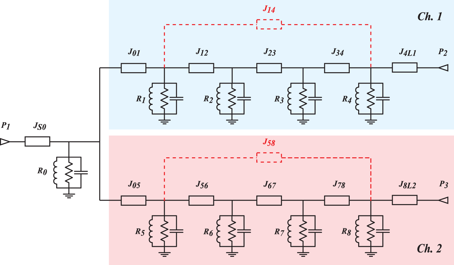
Figure 1 shows the distributed topology, schematic view, and fabricated prototype of the proposed diplexer. In this design, the distributed SIW cavity, folded in two separate PCB layers, is employed to achieve a compact diplexer configuration. As can be seen, each channel of the diplexer consists of four resonators linked to a common resonator (R0). The proposed diplexers are designed and fabricated on two separate PCB substrates of RO4350 (εr = 3.66, h = 0.508 mm, and tan δ = 0.004). The GCPW feed line and resonators R 0, R 1, R 2, R 5, and R 6 are in the top substrate. The resonators R 3, R 4, R 7, and R 8 are in the bottom substrate. In the following sections, the design process, simulations, and results of the diplexer are discussed in detail.
(a) Topology: the couplings of M 14 and M 58 (dashed red lines) are related to negative couplings, (b) top and side view, (c) 3D view, and (d) photo of the fabricated diplexer.

Design procedure
This section outlines the design procedure of the diplexer, which includes the following steps:
1. Define the performance requirements of the diplexer.
2. Derive the coupling matrix (CM) based on the specifications.
3. Verify the extracted CM through the equivalent circuit model (ECM).
4. Translate diplexer parameters into a physical structure.
Specifications
As the first step in the design procedure, we have selected the following specifications for diplexer: a fourth-order Chebyshev band-pass filter, return loss of 20 dB, bandwidth of 1 GHz for each channel, and center frequencies of 27 and 29 GHz for channels 1 and 2, respectively. To enhance the frequency selectivity of the diplexer, two symmetric transmission zeros (TZs) at 26.03 and 28.00 GHz for channel 1 and 28.00 and 30.03 GHz for channel 2 are introduced.
Coupling matrix synthesis
The synthesis process for the star-junction diplexer is based on the methodology presented by Macchiarella in [Reference Macchiarella and Tamiazzo25, Reference Macchiarella and Tamiazzo26]. Table 1 provides the synthesized coupling matrix for the diplexer with the specified configuration. As depicted in Table 1, there is a negative coupling between resonators R 1 and R 4, and also between R 5 and R 8.
Coupling matrix of the diplexer

Equivalent circuit model
The ECM of the diplexer is presented in Fig. 2. In this model, each resonator is represented as a parallel RLC circuit, and inter-resonator couplings are modeled using J-inverters. In order to consider the loss of the diplexer, the unloaded quality factors of the RLC resonators are to 175. The two symmetric transmission zeros per channel are introduced by the negative couplings between the first and last resonators, J 14 and J 58, of the diplexer, thereby improving the frequency selectivity.
Equivalent circuit model of the diplexer (the couplings J 14 and J 58: dashed red lines are related to the negative couplings).

Physical realization of the parameters
The next step is physical realization of the coupling matrix elements. These elements are related to the diplexer parameters such as coupling coefficients (Kij) and the external quality factor (Qe) through equations (1) and (2) [Reference Cameron, Kudsia and Mansour27–Reference Ness29].
 \begin{equation}{k_{ij}} = {{FBW}} \cdot {M_{ij}} = \frac{{f_{\text{h}}^{\text{2}} - f_{\text{l}}^{\text{2}}}}{{f_{\text{h}}^{\text{2}} + f_{\text{l}}^{\text{2}}}}\end{equation}
 \begin{equation}{Q_{\text{e}}} = \frac{1}{{{{FBW}} \cdot M_{S0}^2}} = \frac{{{\omega _0}{\Gamma _{d1}}}}{4}\end{equation}
Here, FBW is the fractional bandwidth, Mij is the coupling coefficient between resonators i and j, and f h and f l are the upper and lower resonant frequencies, respectively. M S0 is the coupling coefficient between the source and the common resonator or between the last resonator and load, and Γd1 is the group delay of the single-port resonator. These equations provide the relationship between these parameters and the simulated results of a one- or two-port setup in High-Frequency Structure Simulator (HFSS).
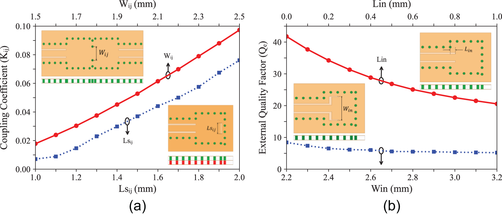
The simulation setup and design curves of the coupling coefficients and external quality factors of the diplexer are shown in Fig. 3. The coupling coefficients k 01, k 12, k 34, k 05, k 56, and k 78 are implemented through iris windows on the common walls between adjacent resonators and controlled by Wij. Similarly, the coupling coefficients k 23 and k 67 are achieved through rectangular slots with a length of Lsij, connecting the corresponding resonators. The negative or electrical coupling coefficients, such as k 14 and k 58, are realized using circular slots between the respective resonators, and controlled by the diameters of the circles, which are not shown here due to the similarity in the design process.
Design curves of the (a) coupling coefficient (Kij) versus Wij and Lsij, and (b) external quality factor (Q e) versus W in and L in.

The input and output external quality factors are physically implemented using extended inset feeds on the 50-ohm grounded coplanar waveguide (GCPW) line. For the input port, a lower value of external quality factor (Q e = 5.1703) is required to cover both channels of the diplexer (26.5–29.5 GHz), and this is controlled by the parameter Win. For the output ports, higher Q e values are needed (Q e = 30.5451 for channel 1 and Q e = 33.2954 for channel 2), which are controlled by the parameter Lin.
The initial values of the physical parameters are selected from the curves presented in Fig. 3, and the space mapping technique [Reference Amari, LeDrew and Menzel30] is employed for efficient fine-tuning after setting the initial values.
Results
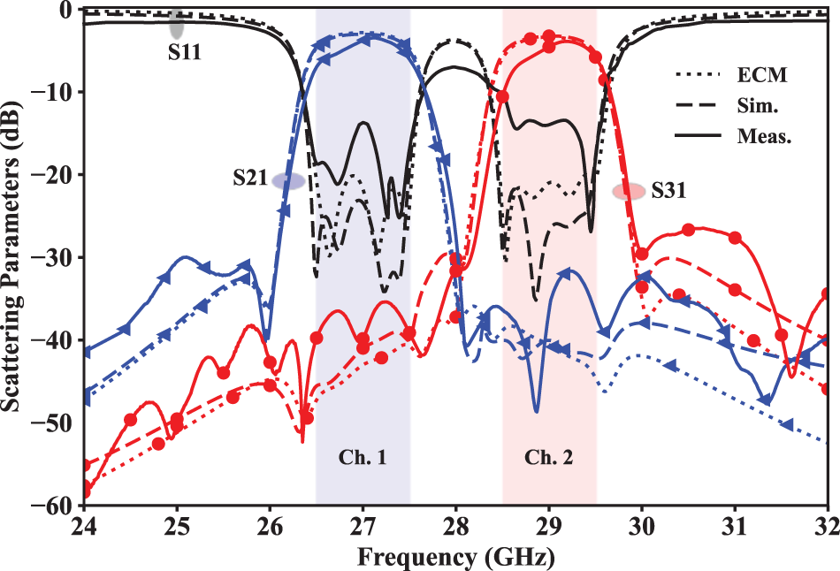
Figure 4 compares the ECM, full-wave simulation, and measured scattering parameters of the diplexer. The simulated return loss of 20 dB is achieved for both channels, while it is about 15 and 12.5 dB, respectively, for channels 1 and 2. The minimum simulated (measured) insertion loss is 3.03 dB (3.47 dB) for channel 1, and 3.24 dB (3.62 dB) for channel 2. As well as, it shows a high frequency selectivity with close-to-band rejection. The results fit all the specifications of the diplexers, which verify the proposed design procedure of the diplexer.
Comparison of the equivalent circuit model (ECM), full-wave simulation, and experimental results of the diplexer.

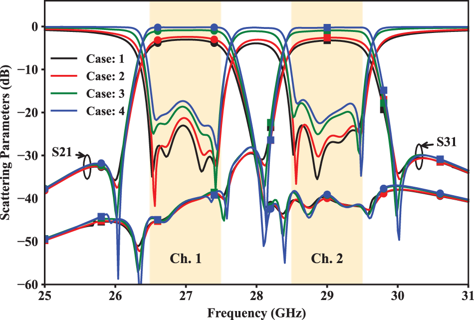
Figure 5 illustrates the impact of substrate and metal losses on the diplexer performance. This investigation studies four combinations of lossy and lossless substrates and metals. RO4350 is used as the lossy substrate, and Sub1, with the same relative permittivity as RO4350 but with a dielectric loss tangent of zero, represents the lossless substrate. Copper and PEC (Perfect Electric Conductor) are used as the lossy and lossless metals, respectively. Table 2 summarizes the case-wise substrate and metal used, along with respective S 21 and S 31 values at 27 and 29 GHz. The results show 0.21 dB (0.25 dB) loss due to leakage and interchannel insulation and matching imperfection, 0.65 dB (0.67 dB) loss due to the conductivity of metal, and 2.2 dB (2.36 dB) loss due to dielectric dissipation at 27 GHz (29 GHz). Material properties are closely examined during this analysis, with insertion loss properties (both transmission and reflection) highlighted and discussed concerning how they dictate the diplexer’s overall effectiveness.
The impact of substrate and metal losses on the diplexer performance.

The summary of the materials and insertion losses

Diplexer-antenna
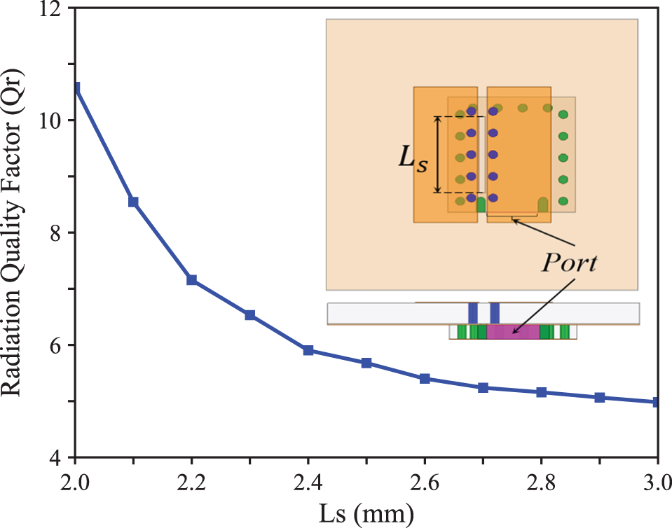
Figure 6 shows the schematic view of the proposed diplexer-antenna, which integrates the ME dipole antenna and designed diplexer in the previous section. In this design, the input port of the diplexer is removed and a rectangular slot is etched on the common resonator of the diplexer (R 0) to excite the ME dipole antenna to realize the radiation performance and external quality factor, which almost equals the antenna’s radiation quality factor, Qr [Reference Lancaster31, Reference Xiang, Chen, Tan and Chu32].
 \begin{equation}{Q_r} = \frac{{{f^2}}}{{\left( {{f^2} - f_0^2} \right)}}.\left[ {\frac{{{{\left| {{S_{11}}\left( f \right)} \right|}^2}{{\left( {1 + \beta } \right)}^2} - {{\left( {1 - \beta } \right)}^2}}}{{1 - {{\left| {{S_{11}}\left( f \right)} \right|}^2}}}} \right]\end{equation}
 \begin{equation}\beta = \frac{{1 \pm \left| {{S_{11}}\left( {{f_0}} \right)} \right|}}{{1 \mp \left| {{S_{11}}\left( {{f_0}} \right)} \right|}}\end{equation}
(a) Topology, (b) top and side view, and (c) 3D view of the proposed diplexer-antenna.

Here, f is any frequency except the resonant frequency (f o), and  $\beta $ is the coupling coefficient between the external circuit and the resonator.
The radiation quality factor Q r indicates how efficiently the antenna radiates energy versus how much energy is stored in the resonator. A lower Q r corresponds to stronger radiation and wider bandwidth, while a higher Q r means weaker radiation and narrower bandwidth. The main parameters affecting Q r are as follows:
• Reflection coefficient ∣S11∣: The depth and sharpness of the S11 resonance directly influence Q r. A sharper resonance yields higher Q r.
• Coupling coefficient β: Determined from ∣S11(f0)∣ it reflects the strength of coupling to free space. Stronger coupling (larger β) lowers Q r.
• Slot length L s: Increasing the slot length enhances radiation and external coupling, reducing Q r. Shorter slots result in higher Qr due to weaker radiation.
Thus, Fig. 7 illustrates how modifying the slot length directly tunes the radiation quality factor of the ME-dipole antenna. The ME dipole antenna provides a wide bandwidth, flat gain, and stable radiation pattern over the frequency [Reference Farahani, Rezaee and Bösch33], which is required for this diplexer-antenna to cover both lower and upper channels. As shown in Fig. 6, this diplexer-antenna is designed on three different PCB layers of RO 4350 with substrate thicknesses of 0.762 mm for layer 1 and 0.508 mm for layers 2 and 3.
Design curve of the radiation quality factor (Qr) versus the length of the slot (L s).

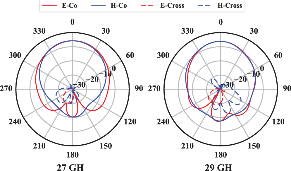
The simulated and measured co- and cross-polar radiation patterns in E- and H-planes at 27 and 29 GHz are shown in Fig. 13, and show a good agreement between them. Also, the cross-polarizations realized gain are below −15 and −11 dBi, respectively, at 27 and 29 GHz. Figure 14 shows the electrical field distribution within the resonators and feed line and the surface current on the patch antennas at 27 and 29 GHz.
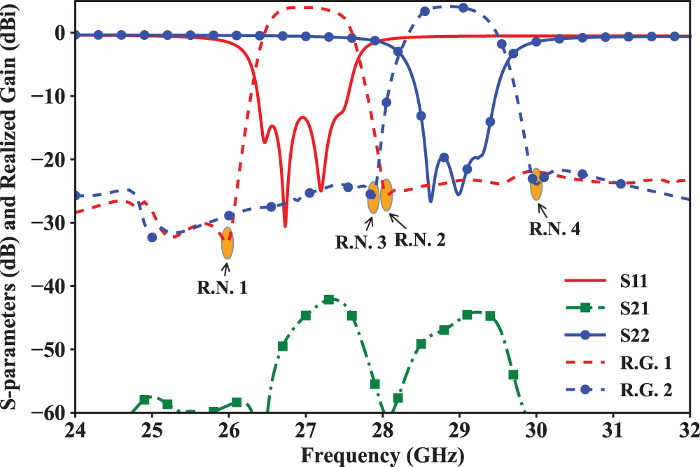
The simulated results of the proposed diplexer-antenna are shown in Figs. 8 and 9. The in-band return loss for channels 1 and 2 is better than 15 and 17 dB, respectively, and the peak realized gain is about 4.1 and 3.8 dBi. The isolation between channels 1 and 2 is better than 40 dB. Also, it shows two radiation nulls at 26.0 and 28.05 GHz for channel 1 and two at 27.9 and 30.0 GHz for channel 2.
Scattering parameters and realized gain of the proposed diplexer-antenna.

Radiation patterns of the diplexer-antenna in E- and H-planes at 27 and 29 GHz.

The simulated co- and cross-polar radiation patterns in E- and H-planes at 27 and 29 GHz are depicted in Fig. 8 and show symmetric and stable results. Also, the cross-polarizations realized gain are below −17 and −12 dBi, respectively, for channels 1 and 2.
Dual-band Filtenna
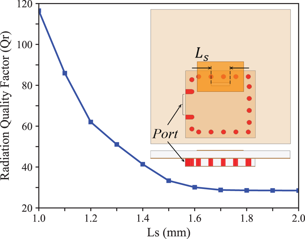
By removing the output ports of the diplexer, etching a rectangular slot on the last resonators of each channel (R 4 and R 8), and loading them with two patch antennas, a dual-band filtenna can be realized. In this filtenna design, each antenna is required to cover only its designated bandwidth. Compared to the diplexer-antenna, this eliminates the need for wideband antennas. The design curve of the radiation quality factor of the patch antenna versus the length of the slot (L s) is shown in Fig. 10. The topology, layout, and fabricated prototype of the proposed dual-band filtenna are illustrated in Fig. 11. To demonstrate the proposed filtenna, it has been fabricated on three separate layers of RO4350 substrate with the same thickness of 0.508 mm for all layers, then stacked and fastened together using screws and conductive paint silver to enhance the ground connection between the different layers.
Radiation quality factor (Q r) of the patch antenna vs. Length of the slot (L s).

Proposed dual-band filtenna: (a) Topology, (b) top and side view, (c) 3D view, and (d) photo of the fabricated prototype.

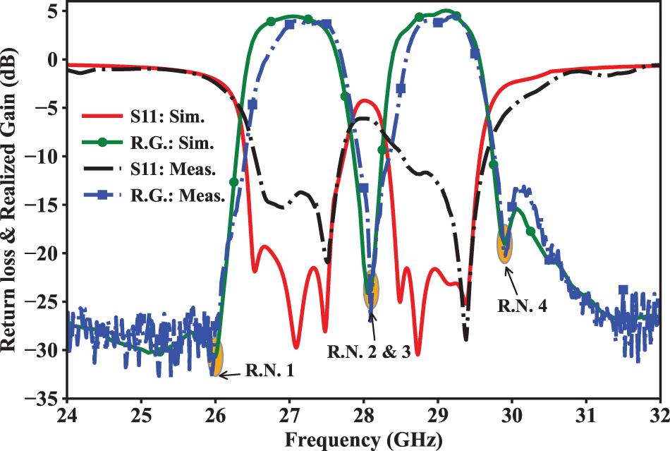
The simulated and measured return loss and realized gain of the dual-band filtenna are presented in Fig. 12. The simulated in-band return loss for the lower frequency band (26.5–27.52 GHz) is 20.53 dB, and for the higher frequency band (28.44–29.45 GHz) is 21.55 dB. The simulated peak realized gain in the lower and higher bands is 4.43 and 5.03 dBi, respectively. The measured return loss for the lower (higher) band in 26.64–27.65 GHz (28.37–29.59 GHz) is 13.72 dB (11.67 dB), and the peak realized gain is 4 dBi (4.5 dBi). Moreover, the four radiation nulls at 26, 28 (two nulls), and 30 GHz enhanced the frequency selectivity and achieved the steep roll-off close-to-band rejection on both sides of the lower and higher bands. The observed variation in behavior within the pass band was attributed to fabrication errors and layer misalignment.
Simulated and measured return loss and realized gain of the dual-band filtenna.

Radiation patterns of the dual-band filtenna in E- and H-planes at (a) 27 GHz and (b) 29 GHz.

E-field distribution and surface current at 27 GHz (left) and 29 GHz (right).

The final dimensions of the proposed dual-band filtenna are listed in Table 3. It should be noted that the proposed configuration can be used to achieve a single-band filtenna array by selecting the symmetric structures as presented in [Reference Rezaee, Farahani and Bösch35]. Table 4 compares the performance of this work and some previous designs in terms of operating frequency, peak realized gain, selectivity, number of resonators and radiating nulls, and size. As depicted, the proposed design offers the best frequency selectivity (lowest F L and F U).
Physical dimensions of the structures

Comparison with other previous works

a Frequency selectivity:  ${F_{\text{L}}} = \frac{{f_{10{\text{dB}}}^L - f_{\Delta 15{\text{dB}}}^L}}{{f_{10{\text{dB}}}^U - f_{10{\text{dB}}}^L}}$, ${F_{\text{U}}} = \frac{{f_{\Delta 15{\text{dB}}}^{\text{U}} - f_{10{\text{dB}}}^{\text{L}}}}{{f_{10{\text{dB}}}^{\text{U}} - f_{10{\text{dB}}}^{\text{L}}}}$ where $f_{10{\text{dB}}}^{\text{L}}$ and $f_{10{\text{dB}}}^{\text{U}}$ are the frequencies at which |S 11| = −10 dB at the lower and upper band edges of the passband, respectively. Similarly, $f_{{{\Delta }}15{\text{dB}}}^{\text{L}}$ and $f_{{{\Delta }}15{\text{dB}}}^{\text{U}}$ represent the lower and upper frequencies with 15 dB attenuation compared to S 21 at ${f_0}$, respectively. Note that smaller values of ${F_{\text{L}}}$ or ${F_{\text{U}}}$ represent better frequency selectivity [Reference Li, Zhao, Tang and Yin21, Reference Xu, Shi, Qing and Chen34].
Conclusion
This work introduces a novel design for a diplexer-antenna and a dual-band filtenna for 5 G mmWave applications. The design stands out for its ability to achieve high isolation and high-frequency selectivity. By integrating a diplexer with ME dipole antennas or microstrip patch antennas, the system effectively combines the functionalities of a diplexer, filter, and antenna. This integration allows each channel’s filtering behavior to be independently designed and fine-tuned. To validate the approach, prototypes were developed and tested for two frequency ranges: 26.5–27.5 and 28.5–29.5 GHz. These designs were based on a fourth-order Chebyshev response and featured symmetric radiation nulls for each band. When fabricated, the dual-band filtenna achieved peak realized gains of 4 and 4.5 dBi for the lower and upper bands, respectively. It also demonstrated excellent performance in suppressing out-of-band signals, with a steep roll-off exceeding 20 dBi. Comparative analysis between simulated and measured results demonstrates good agreement, confirming the efficiency of the proposed method.
Acknowledgements
The Financial support from the Austrian Federal Ministry for Digital and Economic Affairs, the National Foundation for Research, Technology, and Development, and the Christian Doppler Research Association is gratefully acknowledged. And supported by TU Graz Open Access Publishing Fund.
Competing interests
The authors report no conflict of interest.

Behrooz Rezaee received the BSc degree from Tabriz University, Iran, in 2013, the MSc degree from the K.N. Toosi University of Technology, Tehran, Iran, in 2015, and the PhD degree from the Graz University of Technology, Austria. Since January 2023, he has been holding post-doctoral research with the Institute of Microwave and Photonic Engineering. During his studies, he was involved in designing Antenna, Filter, Filterin Antenna (Filtenna), Lens, Phase Array, and MIMO Antenna for highly integrated RF front-ends, and dual-band HF/UHF RFID Antenna.

Wolfgang Bösch (Fellow, IEEE) received the Dipl.-Ing. degree from the Technical University of Vienna, Vienna, Austria, in 1985, the PhD degree from the Graz University of Technology, Graz, Austria, in 1988, and the MBA degree from the School of Management, University of Bradford, Bradford, UK, in 2004. In 2010, he joined the Graz University of Technology to establish the Institute for Microwave and Photonic Engineering. For the last eight years, he was the Dean of the Faculty of Electrical and Information Engineering, which currently incorporates 13 institutes and 20 full professors covering the areas of energy generation and distribution, electronics, and information engineering. He is responsible for the strategic development, budget, and personnel of the faculty. Prior to this, he was the Chief Technology Officer (CTO) of the Advanced Digital Institute, Shipley, U.K. He was also the Director of Business and Technology Integration with RFMD, Newton Aycliffe, UK. For almost ten years, he was with Filtronic plc, Leeds, UK, as the CTO of Filtronic integrated products and the Director of the Global Technology Group. Before joining Filtronic, he held positions at the European Space Agency, Noordwijk, The Netherlands, working on amplifier linearization techniques; MPR-Teltech, Burnaby, BC, Canada, working on monolithic microwave integrated circuit (MMIC) technology projects; and the Corporate Research and Development Group, M/A-COM, Boston, MA, USA, where he worked on advanced topologies for high-efficiency power amplifiers. For four years, he was with DaimlerChrysler Aerospace (currently, Hensoldt), Ulm, Germany, working on T/R modules for airborne radar. He has published more than 180 articles and holds four patents. Prof. Bösch is a fellow of Institution of Engineering and Technology (IET).


 Open access