


1 Introduction
Advancements in laser technology and plasma target design, accompanied by a deeper understanding of acceleration processes, have enabled the present generation of petawatt (PW)-class laser systems to consistently produce high-energy, high-quality and high-current electron beams in plasmas over just a few centimeters[ Reference Kim, Pae, Cha, Kim, Yu, Sung, Lee, Jeong and Lee 1 – Reference Radier, Chalus, Charbonneau, Thambirajah, Deschamps, David, Barbe, Etter, Matras, Ricaud, Leroux, Richard, Lureau, Baleanu, Banici, Gradinariu, Caldararu, Capiteanu, Naziru, Diaconescu, Iancu, Dabu, Ursescu, Dancus, Ur, Tanaka and Zamfir 11 ]. The laser wakefield accelerator (LWFA)[ Reference Tajima and Dawson 12 ] offers a considerably stronger accelerating field than traditional accelerators that rely on radio-frequency (RF) acceleration chamber structures, thereby significantly reducing the size and cost of the accelerator. This technology enables the development of compact, table-top accelerators that can provide higher energy levels with significant potential for driving novel radiation sources[ Reference Albert and Thomas 13 – Reference Corde, Phuoc, Lambert, Fitour, Malka, Rousse, Beck and Lefebvre 15 ]. An important X-ray source derived from the LWFA is betatron radiation, which is produced by electron oscillations in the transverse electromagnetic fields of the plasma during acceleration[ Reference Rousse, Phuoc, Shah, Pukhov, Lefebvre, Malka, Kiselev, Burgy, Rousseau, Umstadter and Hulin 16 – Reference Albert, Lemos, Shaw, Pollock, Goyon, Schumaker, Saunders, Marsh, Pak, Ralph, Martins, Amorim, Falcone, Glenzer, Moody and Joshi 18 ]. Betatron radiation, characterized by a broad spectrum extending into the range of tens of keV[ Reference Esarey, Shadwick, Catravas and Leemans 19 ], has an ultrashort pulse duration of less than 100 fs[ Reference Phuoc, Fitour, Tafzi, Garl, Artemiev, Shah, Albert, Boschetto, Rousse, Kim, Pukhov, Seredov and Kostyukov 9 , Reference Horný, Nejdl, Kozlová, Krůs, Boháček, Petržílka and Klimo 10 ], a low divergence of only a few millirads[ Reference Björklund Svensson, Guénot, Ferri, Ekerfelt, González, Persson, Svendsen, Veisz and Lundh 20 , Reference Cipiccia, Islam, Ersfeld, Shanks, Brunetti, Vieux, Yang, Issac, Wiggins, Welsh, Anania, Maneuski, Montgomery, Smith, Hoek, Hamilton, Lemos, Symes, Rajeev, Shea, Dias and Jaroszynski 21 ], and a source size of several micrometers[ Reference Kneip, McGuffey, Martins, Martins, Bellei, Chvykov, Dollar, Fonseca, Huntington, Kalintchenko, Maksimchuk, Mangles, Matsuoka, Nagel, Palmer, Schreiber, Phuoc, Thomas, Yanovsky, Silva, Krushelnick and Najmudin 22 , Reference Shah, Albert, Phuoc, Shevchenko, Boschetto, Pukhov, Kiselev, Burgy, Rousseau and Rousse 23 ]. The peak brightness of betatron radiation can reach 1022–1023 photons·s−1·mm−2·mrad−2·0.1%BW−l[ Reference Björklund Svensson, Guénot, Ferri, Ekerfelt, González, Persson, Svendsen, Veisz and Lundh 20 – Reference Kneip, McGuffey, Martins, Martins, Bellei, Chvykov, Dollar, Fonseca, Huntington, Kalintchenko, Maksimchuk, Mangles, Matsuoka, Nagel, Palmer, Schreiber, Phuoc, Thomas, Yanovsky, Silva, Krushelnick and Najmudin 22 , Reference Yu, Liu, Wang, Li, Qi, Zhang, Qin, Liu, Fang, Feng, Wu, Ke, Chen, Wang, Xu, Leng, Xia, Li and Xu 24 ]. These sources enable the detection of ultrafast processes across interdisciplinary fields and provide ultra-high-resolution imaging, owing to their exceptional temporal resolution, peak brightness and spatial coherence[ Reference Hojbota, Mirzaie, Kim, Pak, Rezaei-Pandari, Pathak, Jeon, Yoon, Sung, Lee, Kim, Kim and Nam 25 – Reference Guénot, Svendsen, Lehnert, Ulrich, Persson, Permogorov, Zigan, Wensing, Lundh and Berrocal 27 ].
Higher-power lasers enable the production of higher-energy and brighter X-ray sources, as predicted by the scaling law[ Reference Bloom, Streeter, Kneip, Bendoyro, Cheklov, Cole, Döpp, Hooker, Holloway, Jiang, Lopes, Nakamura, Norreys, Rajeev, Symes, Schreiber, Wood, Wing, Najmudin and Mangles 28 ]. The advent of PW-class laser facilities has led to significant advancements in generating high-quality electron beams and X-ray sources. For example, a 4-PW laser was used to produce high-energy betatron radiation with a critical energy of 515 keV, extending to MeV photon energy[ Reference Hojbota, Mirzaie, Kim, Pak, Rezaei-Pandari, Pathak, Jeon, Yoon, Sung, Lee, Kim, Kim and Nam 25 ]. Similarly, a 0.2 PW laser was employed to generate high-brightness betatron radiation for the micro-computed tomography (μCT) imaging of mouse embryos[ Reference Cole, Symes, Lopes, Wood, Poder, Alatabi, Botchway, Foster, Gratton, Johnson, Kamperidis, Kononenko, De Lazzari, Palmer, Rusby, Sanderson, Sandholzer, Sarri, Szoke-Kovacs, Teboul, Thompson, Warwick, Westerberg, Hill, Norris, Mangles and Najmudin 29 ], while 0.6–0.8 PW lasers achieved electron acceleration exceeding 2 GeV and produced betatron X-rays with promising application potential[ Reference Wang, Zgadzaj, Fazel, Li, Yi, Zhang, Henderson, Chang, Korzekwa, Tsai, Pai, Quevedo, Dyer, Gaul, Martinez, Bernstein, Borger, Spinks, Donovan, Khudik, Shvets, Ditmire and Downer 2 ]. These developments demonstrate the capability of PW-class lasers to significantly enhance the critical energy and photon yield of betatron radiation. However, there are limited reports on the use of PW-class lasers that interact with gas targets to produce radiation sources that simultaneously achieve higher photon yields, greater critical energies and smaller source sizes.
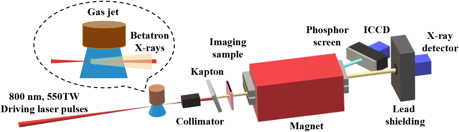
Schematic of the experimental setup for generating a betatron X-ray source via the LWFA and X-ray phase-contrast imaging. A high-power laser (red) was focused at the entrance of a helium gas jet, producing high-energy electron and X-ray beams. A tungsten collimator positioned behind the gas jet effectively blocked bremsstrahlung radiation, whereas the depleted laser pulse was filtered out using either a 50-μm-thick Kapton or 200-μm-thick Al foil. The electron beam (cyan) was deflected using a 180-cm-long dipole magnet with a maximum magnetic field of 1.5 T onto a Lanex PS, where it was imaged using a 14-bit optical camera to measure the electron spectrum. The X-ray beam (yellow) passed through the sample located 40 cm downstream and was imaged onto an X-ray detector, positioned an additional 470 cm away.
This study examines the characteristics of a bright betatron hard X-ray source utilizing the 1 PW/0.1 Hz laser system at the Shanghai Superintense Ultrafast Laser Facility (SULF). This system can produce high-charge, high-energy electron beams with charges exceeding 100 pC and energies exceeding 1 GeV. The resulting betatron X-ray source has a critical energy of 22 ± 5 keV and achieves a maximum flux of up to 4 × 10⁹ photons in the spectral range of 5–30 keV. Furthermore, we demonstrate that the betatron radiation source, with a source root-mean-square (rms) size of 2 μm and bright spatial coherence, is effective for non-destructive testing and imaging, enabling the detection of defects or bubbles in various devices.
2 Experimental setup
The experiment was conducted using the 1 PW/0.1 Hz laser system at SULF[ Reference Zhang, Wu, Hu, Yang, Gui, Ji, Liu, Wang, Liu, Lu, Xu, Leng, Li and Xu 30 ] at the Shanghai Institute of Optics and Fine Mechanics (SIOM). Figure 1 shows a schematic of the experimental setup used to generate a betatron X-ray source via the LWFA. An 800 nm, linearly polarized laser pulse with an energy of 15 J, repetition rate of 0.1 Hz and pulse duration of 28–30 fs was focused 1.75 mm below a pulsed nozzle that produced a high-density helium gas jet. With an f/50 off-axis parabola mirror of 12 m focal length, the focal spot achieved a full width at half maximum (FWHM) of 56 μm. The fractional laser energy within the focus spot was approximately 68% at 1/e2, resulting in a peak intensity of 7.7 × 10¹⁸ W/cm2 and a corresponding normalized amplitude of a 0 ≈ 1.9.
The gas target was produced using an elliptical supersonic nozzle with a long axis of 8.8 mm and short axis of 4.5 mm. The plasma density was varied by adjusting both the gas jet pressure and its timing relative to the arrival of the laser pulse. The plasma density distribution was measured using an optical interferometer[ Reference Wang, Feng, Ke, Yu, Xu, Qi, Chen, Qin, Zhang, Fang, Liu, Jiang, Wang, Wang, Yang, Wu, Leng, Liu, Li and Xu 31 ]. A maximum plasma density ranging (5–8) × 1018 cm−3 could be achieved by varying the pressure of the pure helium gas jet between 5 and 7 bar.
The electron beams, deflected using a 180-cm-long tunable dipole electromagnet with a maximum magnetic field of 1.5 T, were measured using a Lanex phosphor screen (PS) imaged with a 14-bit optical camera. The measurements were performed in a single shot at a distance of 350 cm and were cross-calibrated using a calibrated imaging plate (IP) to determine the electron beam charges. A lead wall built behind the electron spectrometer could eliminate electrons and shield against bremsstrahlung radiation interference.
A tungsten collimator 10 cm in length and 5 mm in diameter was positioned 15 cm away from the gas jet at an acceptance angle of 20 mrad to filter out the bremsstrahlung radiation from low-energy and large-divergence electrons. The betatron X-rays emitted by the electron beams from the LWFA were detected using a 16-bit back-illuminated X-ray charge-coupled device (CCD) (Teledyne Princeton Instruments, SOPHIA-XO:2048B) with a high resolution of 2048 × 2048 pixels, each 13.5 μm in size, offering an exceptional signal-to-noise ratio and rapid readout capabilities. During the measurement of the photon flux with the X-ray CCD in a vacuum, a 200-μm-thick aluminum (Al) foil was placed in front of the CCD as a plasma mirror to reflect the laser. For imaging applications, a 50-μm-thick Kapton foil was positioned in front of the sample as a plasma mirror to reflect the residual laser. For large field-of-view imaging, a Fuji BAS-SR IP, shielded using lead bricks, was used to capture the X-rays passing through a 100-μm-thick Al and 300-μm-thick beryllium (Be) window. The IP was then scanned using a GE Typhoon IP scanner, which provides high-resolution imaging at 10 μm.
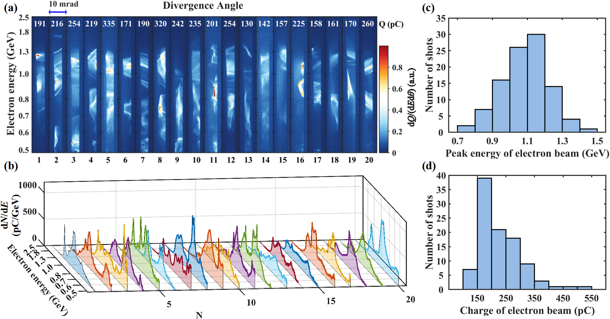
Characterization of high-charge GeV-class electron beams. (a) Raw electron energy spectra of 20 shots at an electron density of n e = 6 × 1018 cm−3. The corresponding charge for each shot is indicated in white above the spectra. (b) Electron spectra angularly resolved in the laser polarization plane, within the range of 0.5–2.5 GeV. (c) Statistical analysis of the peak energy and (d) charge of the electron beam for 100 shots under the same conditions (n e = 6 × 1018 cm−3).
3 Generation of high-charge GeV-class electron beams
In the experiments, laser pulses with a power of approximately 550 TW were focused onto a high-density pure helium jet to generate a high-energy and high-charge electron beam and betatron X-ray radiation. The gas pressure and nozzle position relative to the laser focal point were adjusted to optimize conditions for stable, high-flux betatron X-ray beams. The best results were achieved at a maximum electron density of 7.8 × 1018 cm−3 with the laser focused at the entrance of the helium gas jet. In the plasma, electrons were continuously self-injected and accelerated to high energies owing to laser focusing and the expansion of the bubble. As shown in Figures 2(a) and 2(b), under these conditions, the typical energy spectra of the electron beams exhibited a high-energy peak approaching 1.3 GeV and a low-energy peak above 0.8 GeV. However, this experiment mainly aimed to maximize the betatron radiation yield, which requires that the propagation length of the electron beam exceeds the dephasing length. Consequently, the measured spectra did not accurately reflect the electron energy at maximum betatron radiation emission. Figures 2(c) and 2(d) show the statistical analysis of the peak energy and charge of the electron beam across 100 shots under consistent conditions. Approximately 74% of the electron beams exhibited a maximum energy exceeding 1 GeV, whereas 55% demonstrated a maximum energy in the range of 1–1.2 GeV. Although the charges of the low-energy electrons with energies below 500 MeV were not considered, 55% of the electron beams carried charges exceeding 200 pC for electron energies greater than 500 MeV.
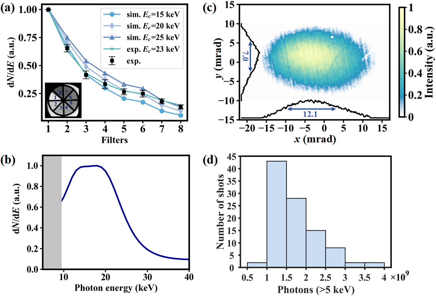
Characterization of betatron radiation. (a) Radiation intensity distribution (black squares) measured through calibrated metallic cut-off filters made from varying thicknesses of Al and Cu foils (see inset). The filters, labeled from 1 to 8, consisted of blank, 400 μm Al foil, and 40, 70, 120, 150, 300 and 500 μm Cu foils, respectively. The calculated intensity distributions are shown using the synchrotron spectra with critical energies E c of 15 keV (circle), 20 keV (diamond) and 25 keV (triangle). (b) Single-shot normalized betatron spectrum with E c = 23 keV, corresponding to the radiation intensity distribution (green stars) through the filters shown in (a). The gray shaded area represents the transmission threshold for the Kapton foil, Al and Be window and air. (c) Betatron radiation divergence with an FWHM of 12.1 mrad × 7.0 mrad. (d) Statistical analysis of the photon counts from X-ray beams for 100 shots, based on the divergence angle shown in (c), corresponding to the electron beams in Figures 2(c) and 2(d).
4 Generation of bright betatron X-rays
The spectral characteristics of the betatron radiation were determined by measuring the intensity distribution of the X-ray beams after passing through an array of filters of varying thicknesses, using a Fuji BAS-SR IP (inset of Figure 3(a)). Assuming the spectrum has a synchrotron-like shape, it can be described by the following equation[ Reference Esarey, Shadwick, Catravas and Leemans 19 ], which is valid for on-axis betatron X-rays:
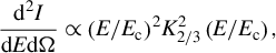 $$\begin{align*}\frac{{\mathrm{d}}^2I}{\mathrm{d}E\mathrm{d}\Omega}\propto {\left(E/{E}_{\mathrm{c}}\right)}^2{K}_{2/3}^2\left(E/{E}_{\mathrm{c}}\right),\end{align*}$$
where K
2/3 is a modified Bessel function of the second kind, E is the photon energy and E
c is the critical energy that determines the shape of the spectrum. Considering the transmission through each filter (Ti
(E)) and the absolutely calibrated response of the IP (R(E)), the X-ray spectrum can be obtained by performing a least-squares fit to the signals detected behind each filter. This is achieved by minimizing ${\sum}_i{\left({P}_{\mathrm{calc},i}-{P}_{\mathrm{meas},i}\right)}^2$
, where
${\sum}_i{\left({P}_{\mathrm{calc},i}-{P}_{\mathrm{meas},i}\right)}^2$
, where ${P}_{\mathrm{meas},i}$
is the measured signal for each filter and
${P}_{\mathrm{meas},i}$
is the measured signal for each filter and ${P}_{\mathrm{calc},i}$
represents the calculated normalized signals for each filter, given by
${P}_{\mathrm{calc},i}$
represents the calculated normalized signals for each filter, given by $\int \frac{{\mathrm{d}}^2I}{\mathrm{d}E\mathrm{d}\Omega}{T}_i(E)R(E)\mathrm{d}E={P}_{\mathrm{calc},i}$
[
Reference Kneip, Nagel, Bellei, Bourgeois, Dangor, Gopal, Heathcote, Mangles, Marquès, Maksimchuk, Nilson, Phuoc, Reed, Tzoufras, Tsung, Willingale, Mori, Rousse, Krushelnick and Najmudin
17
]. Figure 3(a) shows the measured signals for each filter (black squares) and the calculated normalized signals for the synchrotron spectra with critical energies of E
c = 15 keV (circles), E
c = 20 keV (diamonds) and E
c = 25 keV (triangles). Considering the effects of the Kapton foil, transmission window and 15-cm-thick air gap between the transmission window and detector, photons with energies below 9 keV were filtered out. In this experiment, the fitted betatron X-ray spectrum had a critical energy of 22 keV, with a deviation of ±5 keV representing the maximum and minimum critical energy. An example is shown in Figure 3(b) for a peak electron density of 7.8 × 1018 cm−3, where the best fit was obtained for E
c = 23 keV, corresponding to the radiation intensity distribution (green stars) obtained using filters shown in Figure 3(a). The X-ray beam exhibited a near-Gaussian profile with an FWHM divergence of
$\int \frac{{\mathrm{d}}^2I}{\mathrm{d}E\mathrm{d}\Omega}{T}_i(E)R(E)\mathrm{d}E={P}_{\mathrm{calc},i}$
[
Reference Kneip, Nagel, Bellei, Bourgeois, Dangor, Gopal, Heathcote, Mangles, Marquès, Maksimchuk, Nilson, Phuoc, Reed, Tzoufras, Tsung, Willingale, Mori, Rousse, Krushelnick and Najmudin
17
]. Figure 3(a) shows the measured signals for each filter (black squares) and the calculated normalized signals for the synchrotron spectra with critical energies of E
c = 15 keV (circles), E
c = 20 keV (diamonds) and E
c = 25 keV (triangles). Considering the effects of the Kapton foil, transmission window and 15-cm-thick air gap between the transmission window and detector, photons with energies below 9 keV were filtered out. In this experiment, the fitted betatron X-ray spectrum had a critical energy of 22 keV, with a deviation of ±5 keV representing the maximum and minimum critical energy. An example is shown in Figure 3(b) for a peak electron density of 7.8 × 1018 cm−3, where the best fit was obtained for E
c = 23 keV, corresponding to the radiation intensity distribution (green stars) obtained using filters shown in Figure 3(a). The X-ray beam exhibited a near-Gaussian profile with an FWHM divergence of ${\theta}_x\times {\theta}_y$
= 12.1 mrad × 7.0 mrad, as shown in Figure 3(c). This corresponded to the wiggler parameters of
${\theta}_x\times {\theta}_y$
= 12.1 mrad × 7.0 mrad, as shown in Figure 3(c). This corresponded to the wiggler parameters of $K=\theta \gamma$
, Ky
= 13.7 and Kx
= 23.7 for a simultaneously measured electron beam energy of E
electron = 1.0 GeV.
$K=\theta \gamma$
, Ky
= 13.7 and Kx
= 23.7 for a simultaneously measured electron beam energy of E
electron = 1.0 GeV.
The photon count measured using the X-ray CCD can be converted into the corresponding photon number with the critical energy determined and the synchrotron-like spectrum of E c = 22 keV. The quantum efficiency (q CCD) of the X-ray CCD strongly depends on the photon energy, with high responsivity in the energy range of 0.01–30 keV. The gain of the X-ray CCD (G CCD), which is related to the analog-to-digital conversion (ADC), defines the number of photoelectrons created by each photon, corresponding to the energy deposited on the chip. In the high-gain setting, the X-ray CCD has a gain of 0.93 eV/count, with an ADC speed of 1 MHz, as provided by the manufacturer. The radiation received is related to the CCD count as follows[ Reference Ju, Genoud, Ferrari, Dadoun, Paradkar, Svensson, Wojda, Burza, Persson, Lundh, Andreev, Wahlström and Cros 32 ]:
 $$\begin{align*}{C}_{\mathrm{CCD}}={\int}_{E_1}^{E_2}\frac{{\mathrm{d}}^2I}{\mathrm{d}E\mathrm{d}\Omega}{T}_{\mathrm{total}}{q}_{\mathrm{CCD}}E/{G}_{\mathrm{CCD}}\mathrm{d}E,\end{align*}$$
where C CCD represents the CCD counts measured in the experiment and T total is the total transmission of the 200-μm-thick Al foil. The integration bounds of the CCD counting equation account for the transmittance of the Al foil and quantum efficiency of the CCD camera. Given the pixel size of 13.5 μm and the distance between the source and detector, the photon number per solid angle can be further calculated. The total photon number can then be derived from the divergence angle of the X-ray beam Gaussian profile, as measured in the experiments. Based on the 100 shots from the experimental results, considering both the critical energy error and shot-to-shot variation, the average photon flux was estimated to be 8.3 × 10¹² photons per steradian (for photons with an energy range of 5–30 keV), with a standard deviation (SD) of 2 × 10¹¹ photons per steradian. The X-ray CCD was positioned 470 cm downstream from the source and shielded by a 200-μm-thick Al foil, resulting in a maximum total number of approximately 4 × 10⁹ photons (5–30 keV) within the region defined by ±3 × SD of the FWHM divergence. As shown in Figure 3(d), from a statistical sample of 100 shots, over 98% of the shots contained more than 1 × 10⁹ photons (5–30 keV) and over 28% of the shots contained more than 2 × 10⁹ photons (5–30 keV).
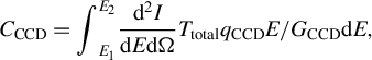
Peak brightness, photon number and critical energy of the betatron X-ray source described in this work compared with the results in Refs. [Reference Wang, Zgadzaj, Fazel, Li, Yi, Zhang, Henderson, Chang, Korzekwa, Tsai, Pai, Quevedo, Dyer, Gaul, Martinez, Bernstein, Borger, Spinks, Donovan, Khudik, Shvets, Ditmire and Downer2, Reference Rousse, Phuoc, Shah, Pukhov, Lefebvre, Malka, Kiselev, Burgy, Rousseau, Umstadter and Hulin16, Reference Kneip, Nagel, Bellei, Bourgeois, Dangor, Gopal, Heathcote, Mangles, Marquès, Maksimchuk, Nilson, Phuoc, Reed, Tzoufras, Tsung, Willingale, Mori, Rousse, Krushelnick and Najmudin17, Reference Cipiccia, Islam, Ersfeld, Shanks, Brunetti, Vieux, Yang, Issac, Wiggins, Welsh, Anania, Maneuski, Montgomery, Smith, Hoek, Hamilton, Lemos, Symes, Rajeev, Shea, Dias and Jaroszynski21, Reference Kneip, McGuffey, Martins, Martins, Bellei, Chvykov, Dollar, Fonseca, Huntington, Kalintchenko, Maksimchuk, Mangles, Matsuoka, Nagel, Palmer, Schreiber, Phuoc, Thomas, Yanovsky, Silva, Krushelnick and Najmudin22, Reference Hojbota, Mirzaie, Kim, Pak, Rezaei-Pandari, Pathak, Jeon, Yoon, Sung, Lee, Kim, Kim and Nam25, Reference Wenz, Schleede, Khrennikov, Bech, Thibault, Heigoldt, Pfeiffer and Karsch26, Reference Bloom, Streeter, Kneip, Bendoyro, Cheklov, Cole, Döpp, Hooker, Holloway, Jiang, Lopes, Nakamura, Norreys, Rajeev, Symes, Schreiber, Wood, Wing, Najmudin and Mangles28, Reference Cole, Symes, Lopes, Wood, Poder, Alatabi, Botchway, Foster, Gratton, Johnson, Kamperidis, Kononenko, De Lazzari, Palmer, Rusby, Sanderson, Sandholzer, Sarri, Szoke-Kovacs, Teboul, Thompson, Warwick, Westerberg, Hill, Norris, Mangles and Najmudin29, Reference Albert, Pollock, Shaw, Marsh, Ralph, Chen, Alessi, Pak, Clayton, Glenzer and Joshi33–Reference Schnell, Sävert, Uschmann, Reuter, Nicolai, Kämpfer, Landgraf, Jäckel, Jansen, Pukhov, Kaluza and Spielmann37].
The X-ray parameters measured in this experiment are compared with previous betatron results in Refs. [Reference Wang, Zgadzaj, Fazel, Li, Yi, Zhang, Henderson, Chang, Korzekwa, Tsai, Pai, Quevedo, Dyer, Gaul, Martinez, Bernstein, Borger, Spinks, Donovan, Khudik, Shvets, Ditmire and Downer2, Reference Rousse, Phuoc, Shah, Pukhov, Lefebvre, Malka, Kiselev, Burgy, Rousseau, Umstadter and Hulin16, Reference Kneip, Nagel, Bellei, Bourgeois, Dangor, Gopal, Heathcote, Mangles, Marquès, Maksimchuk, Nilson, Phuoc, Reed, Tzoufras, Tsung, Willingale, Mori, Rousse, Krushelnick and Najmudin17, Reference Cipiccia, Islam, Ersfeld, Shanks, Brunetti, Vieux, Yang, Issac, Wiggins, Welsh, Anania, Maneuski, Montgomery, Smith, Hoek, Hamilton, Lemos, Symes, Rajeev, Shea, Dias and Jaroszynski21, Reference Kneip, McGuffey, Martins, Martins, Bellei, Chvykov, Dollar, Fonseca, Huntington, Kalintchenko, Maksimchuk, Mangles, Matsuoka, Nagel, Palmer, Schreiber, Phuoc, Thomas, Yanovsky, Silva, Krushelnick and Najmudin22, Reference Hojbota, Mirzaie, Kim, Pak, Rezaei-Pandari, Pathak, Jeon, Yoon, Sung, Lee, Kim, Kim and Nam25, Reference Wenz, Schleede, Khrennikov, Bech, Thibault, Heigoldt, Pfeiffer and Karsch26, Reference Bloom, Streeter, Kneip, Bendoyro, Cheklov, Cole, Döpp, Hooker, Holloway, Jiang, Lopes, Nakamura, Norreys, Rajeev, Symes, Schreiber, Wood, Wing, Najmudin and Mangles28, Reference Cole, Symes, Lopes, Wood, Poder, Alatabi, Botchway, Foster, Gratton, Johnson, Kamperidis, Kononenko, De Lazzari, Palmer, Rusby, Sanderson, Sandholzer, Sarri, Szoke-Kovacs, Teboul, Thompson, Warwick, Westerberg, Hill, Norris, Mangles and Najmudin29, Reference Albert, Pollock, Shaw, Marsh, Ralph, Chen, Alessi, Pak, Clayton, Glenzer and Joshi33–Reference Schnell, Sävert, Uschmann, Reuter, Nicolai, Kämpfer, Landgraf, Jäckel, Jansen, Pukhov, Kaluza and Spielmann37] in Figure 4. Higher-power lasers produce more energy and brighter X-rays. The high photon yields observed in our experiment could be attributed to the high energy and charge of the electron beam generated by the LWFA. Although the critical energies were not significantly enhanced because of the medium electron transverse oscillation amplitude, a relatively small source size and high peak brightness were achieved.
5 Particle-in-cell simulation
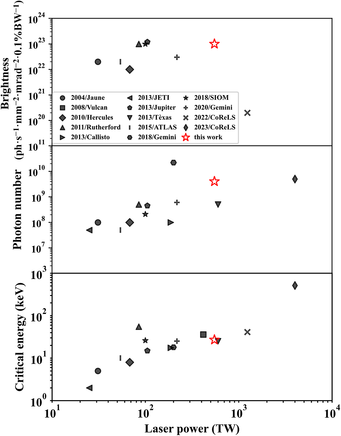
Quasi-three-dimensional numerical simulations were conducted using the Fourier–Bessel particle-in-cell (FBPIC) code[ Reference Lehe, Kirchen, Andriyash, Godfrey and Vay 38 , Reference Jalas, Dornmair, Lehe, Vincenti, Vay, Kirchen and Maier 39 ] to analyze the experimental results. The simulation parameters closely matched the experimental conditions, with a linearly polarized pulse characterized by a wavelength of λ 0 = 0.8 μm, normalized amplitude of a 0 = 1.9, pulse duration of τ = 30 fs and focal spot radius of ω 0 = 48 μm, which was focused 1.25 mm into the plasma. The longitudinal and transverse window sizes were set to 80 and 135 μm, respectively. The grid cell sizes were defined as Δz = 0.05 μm and Δr = 0.135 μm, with 16 macroparticles per cell used in the simulations. The longitudinal electron density profile increased linearly from zero to n e = 2.8 × 1018 cm−3 over the first 1.4 mm, subsequently following a Gaussian distribution with a peak electron density of 7.8 × 1018 cm−3 over the next 7.0 mm, and finally decreasing linearly from 2.8 × 1018 cm−3 to 0 over the next 1.4 mm. The characteristics of the betatron radiation emission from the simulation were determined by applying a post-processing analysis using the SynchRad[ Reference Andriyash 40 ] code, based on the Fourier-transformed Liénard–Wiechert potentials[ Reference Jackson and Fox 41 ], to the electron trajectories. The central energy of the electron beams was approximately 0.8 GeV and the maximum electron beam energy reached up to 1.2 GeV.
Figure 5(a) illustrates the energy evolution of the electron beam, showing the continuous self-injection of electrons into the wakefield. The electrons at the front of the bunch continuously gained energy from the accelerating field of the bubble and eventually entered the decelerating field, where their energies gradually decreased from 1.35 to 1.20 GeV or even lower. Meanwhile, the electrons injected at the later stages continued to be influenced by the acceleration field, resulting in a continuous increase in their energy. Figure 5(b) depicts the typical trajectories of the injected electrons as they evolved within the plasma. The electrons at the front of the bunch exhibited excellent collimation, with oscillation amplitudes within 1.5 μm. These electrons radiated more photons over the same plasma length because of their larger number of oscillation periods. In contrast, the electrons injected at the tail of the bunch were influenced by the wiggling of the electron bunch in the bubble and laser energy depletion, resulting in significantly higher oscillation amplitudes and longer oscillation wavelengths than those of the head electrons. Figures 5(c) and 5(d) present the calculated X-ray spectrum as a function of the energy and angle, with a peak on-axis at 5 keV extending up to 100 keV and a critical energy of 26 keV. A total of 5.99 × 10⁹ photons were predicted between 5 and 100 keV, and 4.86 × 10⁹ photons between 5 and 30 keV, which corresponded to the photon yield measured using the X-ray CCD within the experimental energy range of 5–30 keV. Figure 5(e) illustrates the angular distribution of the radiation, featuring an FWHM divergence of 11.57 mrad × 4.32 mrad.
Simulation of betatron radiation. (a) Energy evolution of the electron beam within the plasma simulated using the FBPIC code. (b) Trajectories of the 20,000 tracked electrons. (c) Betatron X-ray spectrum calculated using the SynchRad code. (d) Angularly and spectrally resolved X-ray flux, exhibiting a peak on-axis at 5 keV with a tail extending to 100 keV. (e) X-ray beam profile of spectral integration, revealing an elliptical shape aligned with the direction of laser polarization.
The simulation results showed that the beam-loading field caused by the high charge at the head of the electron beam reduced the acceleration gradient. Consequently, although the electrons at the tail of the beam had relatively large oscillation amplitudes owing to laser self-focusing and rapid bubble expansion, their energy remained low during oscillation, resulting in a minimal contribution to the overall radiation. In contrast, electrons at the head of the beam reached high-energy regions in the plasma more quickly, due to the higher acceleration gradient at the tail of the bubbles. In the interaction region, these high-energy electrons experienced more oscillation periods, thereby dominating the radiation output. Considering the oscillation amplitude of the head electron, the radiation source size was determined to be ${\omega}_{\mathrm{rms}}$
= 2 μm, with a divergence of 11.57 mrad × 4.32 mrad and radiation duration of 40 fs, corresponding to a 12-μm-long electron bunch. Base on this, we assumed that the maximum peak brightness achieved can reach up to 1.0 × 10²³ photons·s−1·mm−2·mrad−2·0.1%BW−l.
${\omega}_{\mathrm{rms}}$
= 2 μm, with a divergence of 11.57 mrad × 4.32 mrad and radiation duration of 40 fs, corresponding to a 12-μm-long electron bunch. Base on this, we assumed that the maximum peak brightness achieved can reach up to 1.0 × 10²³ photons·s−1·mm−2·mrad−2·0.1%BW−l.
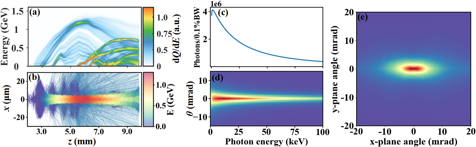
Measurement of the X-ray source size using the shadow of a half-plane on the detector. The measured intensity distribution (black squares) is integrated along the edge of the half-shadow (inset), and the error bars represent the SD of intensity at different positions. The simulated intensity distributions used Fresnel diffraction modeling for a source with a synchrotron spectrum critical energy of E c = 22 keV and Gaussian intensity distributions with rms radii of ω rms = 2 μm (solid red), 4 μm (dashed green) and 6 μm (dotted blue). Gray shading indicates critical energy error.
6 X-ray imaging beamline
This X-ray source can provide ultra-high resolution for phase-contrast imaging due to its micrometer-scale source size. To quantify the source size more precisely, we recorded a half-plane shadow of the object, as shown in the inset of Figure 6. The object was a 3-mm-thick Kapton with a transmission of less than 6% below 50 keV, closely resembling an ideal step function. Fresnel diffraction[ Reference Kneip, McGuffey, Martins, Martins, Bellei, Chvykov, Dollar, Fonseca, Huntington, Kalintchenko, Maksimchuk, Mangles, Matsuoka, Nagel, Palmer, Schreiber, Phuoc, Thomas, Yanovsky, Silva, Krushelnick and Najmudin 22 , Reference Schnell, Sävert, Uschmann, Jansen, Kaluza and Spielmann 42 ] was employed to model the size of the betatron radiation source accurately, with the diffraction fringe details depending on the size, spectral distribution and geometry of the experimental setup. For broadband betatron radiation, only the first diffraction fringe was clearly visible; as the source size decreased, the contrast of this fringe increased. Consequently, the source size could be determined by analyzing the first diffraction fringe at the edge of the shadow of the object. Figure 6 presents a typical experimental intensity distribution, along with several modeled distributions based on a Gaussian intensity profile and synchrotron spectrum. Assuming a critical energy of E c = 22 keV and an rms intensity radius of ω rms = 2 μm, the solid red curve in Figure 6 provides the best fit to the emergence, amplitude and width of the first diffraction fringe, which is consistent with the simulation results.
Imaging of samples using betatron radiation. (a) X-ray image of the Gilder fine square mesh grids (1000-mesh). (b) Optical microscope image of the mesh grids, showing 19-μm grid holes and 6-μm grid ribs. (c) Intensity distribution within the red box in (a), demonstrating that the imaging system resolution is better than 6 μm. (d) X-ray image of an electronic chip. (e) Partially enlarged view of the red box in (d). (f) Line-out from the region of interest marked by the red line in (e).
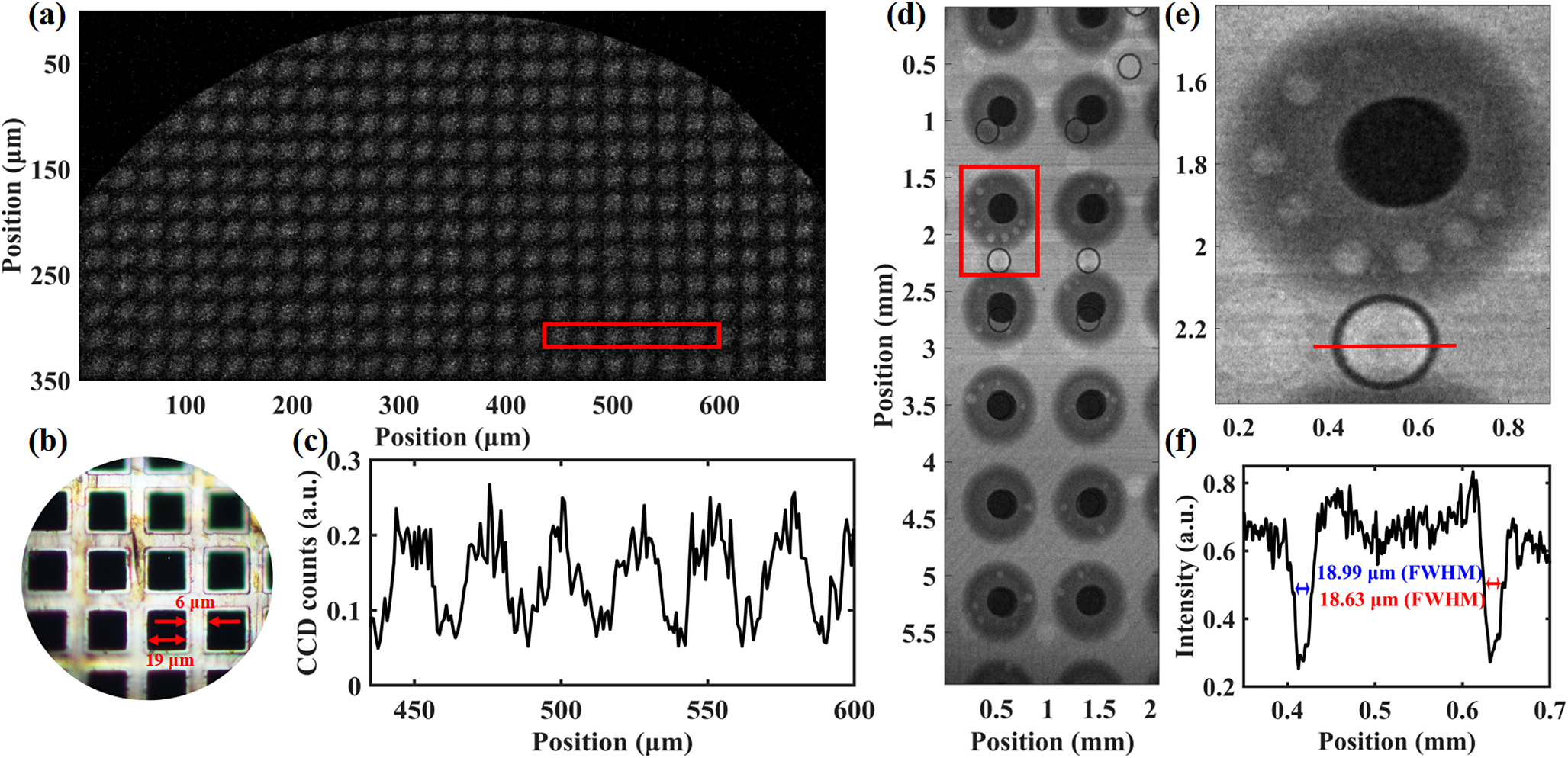
With a source rms size of 2 μm, betatron X-rays can achieve coherent lengths greater than 10 μm over a propagation distance of only a few tens of centimeters, making them well-suited for imaging a wide range of material samples. For samples that require high spatial resolution, the experimental imaging system must be configured with a large magnification factor to satisfy these stringent demands. The betatron radiation imaging setup is shown in Figure 1. The imaging samples were positioned approximately 40 cm behind the gas jet and the X-ray detector was placed at a distance of about 4.7 m, enabling the imaging system to achieve a magnification factor of M = 11.75. The detector resolution of the imaging system was nearly 1.15 μm (X-ray CCD) and 0.85 μm (IP)[ Reference Hussein, Senabulya, Ma, Streeter, Kettle, Dann, Albert, Bourgeois, Cipiccia, Cole, Finlay, Gerstmayr, González, Higginbotham, Jaroszynski, Falk, Krushelnick, Lemos, Lopes, Lumsdon, Lundh, Mangles, Najmudin, Rajeev, Schlepütz, Shahzad, Smid, Spesyvtsev, Symes, Vieux, Willingale, Wood, Shahani and Thomas 43 ]. Considering the source size and maximum resolution of the detector, the overall imaging resolutions were 2.2 μm (X-ray CCD) and 20 μm (IP). The X-ray CCD imaging results are presented in Figures 7(a) and 7(d). As shown in Figure 7(b), the width of the 1000 mesh grid holes was 19 μm, while that of the grid ribs was 6 μm, indicating that each square aperture in the gold mesh corresponded to a width of 25 μm. Figure 7(c) shows the intensity distribution within the red box in Figure 7(a), demonstrating that the imaging system has a high spatial resolution capability of better than 6 μm.
Hard X-ray sources offer high energy and resolution, enabling them to penetrate material surfaces and reveal their internal structures. In this experiment, betatron radiation was used for the non-destructive testing of electronic components. To accommodate the need for large field-of-view imaging, we selected the Fuji BAS-SR IP as the X-ray detector. As shown in Figures 7(d) and 7(e), bubbles and misalignment were clearly visible in the solder joints of the electronic chip. In Figure 7(f) , narrow coils with widths of 18.81 ± 0.18 μm (FWHM) were distinctly resolved, exhibiting a fringe contrast of $\left({I}_{\mathrm{max}}-{I}_{\mathrm{min}}\right)/\left({I}_{\mathrm{max}}+{I}_{\mathrm{min}}\right)=0.44$
.
$\left({I}_{\mathrm{max}}-{I}_{\mathrm{min}}\right)/\left({I}_{\mathrm{max}}+{I}_{\mathrm{min}}\right)=0.44$
.
7 Conclusion
This study presents a betatron X-ray source beamline with high photon flux and critical energy, utilizing the SULF-1 PW laser system to drive the wakefield and generate high-energy electron beams exceeding hundreds of pC with energies exceeding 1 GeV. Firstly, the betatron radiation spectrum was diagnosed, revealing a critical energy of 22 ± 5 keV. Combined with the radiation intensity distribution, the FWHM divergence angles were 12.1 mrad × 7.0 mrad. The maximum photon flux in the spectral range of 5–30 keV was estimated to be up to 4 × 10⁹ photons per laser shot. The simulation results based on experimental parameters agreed closely with the measured outcomes, and the peak brightness reached up to 1.0 × 10²³ photons·s−1·mm−2·mrad−2·0.1%BW−l. Secondly, the source rms size of 2 μm and imaging resolution of the betatron source were measured and assessed using various imaging samples. In the future, we aim to explore the application of betatron radiation sources in diagnosing ultrafast processes across various multidisciplinary fields.
Acknowledgements
The authors thank Changquan Xia and Lulin Fan for discussions and assistance. This work was supported by the National Natural Science Foundation of China (Grant Nos. 12388102, 12225411, 12105353 and 12174410), the CAS Project for Young Scientists in Basic Research (Grant No. YSBR060), the Program of Shanghai Academic Research Leader (Grant No. 22XD1424200), the State Key Laboratory Program of the Chinese Ministry of Science and Technology, the CAS Youth Innovation Promotion Association (Grant No. 2022242) and the Strategic Priority Research Program of the Chinese Academy of Sciences (Grant Nos. XDB0890201 and XDB0890202). Special thanks to the staff at the SULF who provided the laser operation and mechanical, electrical and administrative support throughout the experiments.


 Open access