


Introduction
For next-generation wireless systems, Wi-Fi 7 will use 4096-QAM in a 6-GHz frequency standard to increase the channel capacity and spectral efficiency. The IEEE 802.11be (Wi-Fi 7) standard draft sets a −38 dB requirement on the transmitter error vector magnitude (EVM) for 4096-QAM [Reference Garcia-Rodriguez, López-Pérez, Galati-Giordano and Geraci1]. The NHK (Nippon Housou Kyoukai) also proposed a required carrier to noise (C/N) ratio of around 31 dB for 4096-QAM 8k television transmission [2]. However, as the carrier frequency goes higher, the EVM measurement floor goes higher from −46 dB at 5.95 GHz to −36 dB at 26 GHz [3]. This paper will study the possibility of using 4096-QAM in a 38-GHz millimeter-wave (MMW) system that has a carrier frequency about 6–7 times higher than Wi-Fi 7.
With the Hartley architecture, in order to get good image rejection performance, the amplitudes of the I (in-phase)-path and the Q (quadrature)-path should be the same, and the phase difference between the I-path and the Q-path should be 90°. As a result, low I/Q mismatch is important when it comes to achieving good image rejection performance [Reference Lin, Yang, Tsai, Huang and Wang4,Reference Tsai and Huang5]. In addition, EVM can be affected by many factors, one of which being I/Q mismatch. I/Q mismatch can result in the constellation diagram being distorted [Reference Tsai, Liao, Hsiao and Wang6]. The conventional configuration of the 45° LO power splitter in sub-harmonic mixer utilizes capacitors and inductors. However, it is sensitive to process variation, which is unavoidable in semiconductor manufacturing. The larger phase imbalance caused by process variation can lead to substantial degradation in the performance of the system.
This paper proposes a transmission line based 45° LO power splitter, which replaces the capacitors and inductors with a shunt 90° transmission line at 19 GHz. This configuration is attractive not only because of its design simplicity and easy implementation, but also its ability to greatly reduce the effect of process variation.
Circuit design
Sub-harmonic mixer
The schematic of the proposed demodulator is illustrated in Fig. 1. The LO signal is divided by a 45° LO power splitter into the I (in-phase)-path and the Q (quadrature)-path. On each of the I-path and the Q-path, a doubly balanced sub-harmonic mixer is utilized along with LO/IF buffers. This mixer configuration is a simplified version based on [Reference Tsai and Huang5]. By simplifying the structure and omitting the usage of transistors at RF, there's no need for RF bias network. Only the RF baluns and the power divider are needed at the RF port. By selecting the drain bias to be 0 V, bias network at the IF port can be simplified as well. This configuration has the benefit of high spur suppression [Reference Tsai and Huang5].
Schematic of the proposed demodulator, which is composed of a 45° LO power splitter, two quadrature dividers, two doubly balanced sub-harmonic mixers, LO/IF buffers and Marchand baluns at the RF port. Phase of LO signal is labeled using red numbers.

When deciding the transistor size and gate bias condition of the mixer, transistor width of 2 μm (65-nm) and Vg of 0.2 V is chosen for an initial selection. Figure 2(a) plots the conversion gain (CG) under different fingers from 2 to 20 (the term “finger” means how many gates a transistor has). As can be observed, fingers from 14 to 20 have higher CG under the same LO power.
Simulated conversion gain versus LO input power. (a) different finger number (transistor width of 2 μm and Vg = 0.2 V is chosen for an initial selection); (b) different gate bias (transistor size of 2 μm × 14 fingers is decided).
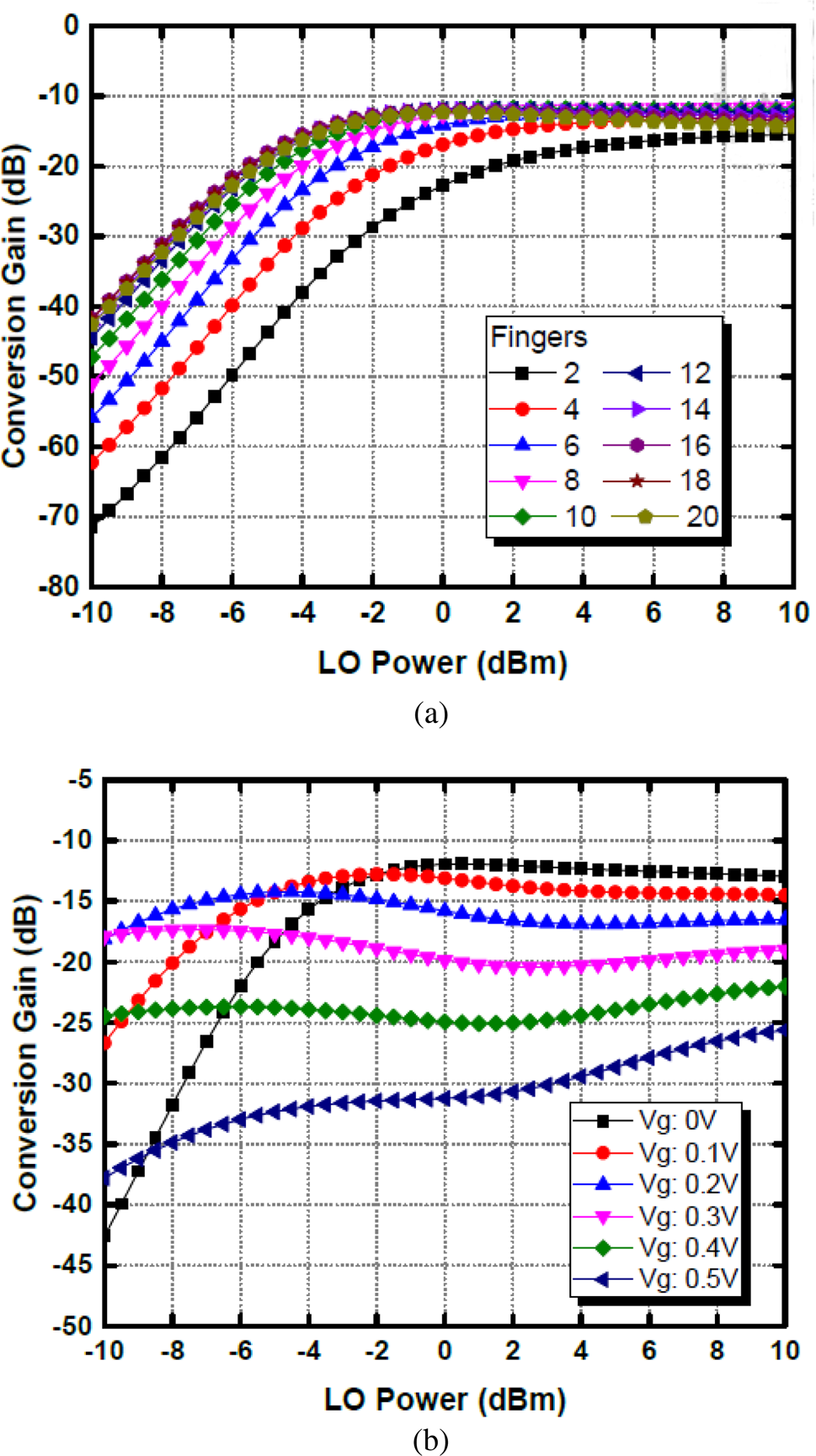
Therefore, we focus on the size of 2 μm × 14 fingers (width × fingers). Figure 2(b) plots the simulation results of CG versus LO power under different gate bias. It can be observed that the highest CG can be obtained with Vg = 0 V over 0 to 10 dBm LO power. To get maximum CG, device size of 2 μm × 14 fingers and Vg = 0 V are chosen.
IF/LO buffer design
Two stage inverter buffer amplifiers are added at the IF ports as IF buffer amplifiers to increase CG. The schematic of an IF buffer amplifier is shown in Fig. 3(a). VDD is set to 1.0 V to get maximum power and prevent transistors breakdown. For the first stage of the IF buffer amplifiers, the transistor sizes are 4 μm × 16 fingers (PMOS) and 4 μm × 10 fingers (NMOS). For the second stage of the IF buffer amplifiers, the transistor sizes are 4 μm × 30 fingers (PMOS) and 4 μm × 20 fingers (NMOS). Rf is 500 Ohms. The IF buffers can provide 20 dB gain with a 3-dB bandwidth of 5 GHz, and its power consumption is 37 mW.
(a) Schematic of IF buffer amplifier; (b) Schematic of LO buffer amplifier.

The proposed demodulator utilizes doubly balanced sub-harmonic mixers, each of which composes of 8 transistors. Because each of the I-path and the Q-path has a mixer, a total of 16 transistors are needed. Large LO power is needed to drive such a large number of transistors. To ease the burden of the LO power requirement, common source amplifiers with high impedance load are used as LO buffers, which amplify the voltage swing to switch transistors easier. Figure 3(b) shows the schematic of a LO buffer amplifier. Gate bias (Vg) is set to 0.6 V and device size of 2 μm × 10 fingers is chosen. As shown in Fig. 4, LO buffer can significantly lower the LO input power requirement, raising CG at 6 dBm LO power from −19 to 2.5 dB.
Simulated conversion gain vs LO power with and without LO buffers.

Passive components
Passive components play an important role in mixer design. When designing a sub-harmonic mixer, a passive component occupies a lot of chip area. To make the layout more compact, adjusting the size and shape of each component is necessary.
Amplitude imbalance and phase error can significantly affect the image rejection ratio (IRR) of a modulator/demodulator [Reference Lin, Yang, Tsai, Huang and Wang4]. Hence at the LO port, it is important to design a four-way quadrature divider with minimum amplitude imbalance and low phase error. The LO signal is divided by a 45° LO power splitter into the I-path and the Q-path. On each of the I-path and Q-path, there is a four-way quadrature divider. A four-way quadrature divider is composed of two baluns and one 90° coupler. Because of sub-harmonic mixer architecture, the four-way quadrature divider is designed at a center frequency of 19 GHz. Its amplitude imbalance under 0.1 dB from 17 to 20 GHz.
At RF port, RF Marchand baluns are designed at a center frequency of 38 GHz.
45° LO power splitter
A mixer not only down-converts the desired signal but also the image signal. A 45° LO power splitter is used to separate the LO signal into the I-path and the Q-path, creating a 45° phase difference between the LO signals in these paths. The 45° phase difference becomes 90° phase difference when the sub-harmonic mixer mixes the 2LO signals with the RF signals to generate the IF signals, thus cancelling the image signal. Ideally, the phase difference between the output ports of the 45° power splitter should be 45°. The more the phase difference deviates from 45°, the higher the I/Q mismatch at the LO port, which dominates the IRR. As a result, 45° LO power splitter is a key component when designing modulators and demodulators [Reference Lin, Yang, Tsai, Huang and Wang4–Reference Hayashi, Okazaki, Kanda, Hirota and Muraguchi9].
The circuit configuration of the conventional 45° power splitter is shown in Fig. 5(a). It composes of a Wilkinson divider, a delay line with electrical length of 45°, two capacitors and one inductor. This configuration is more sensitive to process variation. That is, if the capacitance value deviates from the optimal value, the output phase difference is affected heavily. In order to realize a 45° power splitter less sensitive to process variation, the two capacitors and one inductor are replaced with a short stub with electrical length of 90° at 19 GHz, as shown in Fig. 5(b). According to the quarter-wavelength transmission line theory, the input impedance of the short stub is in theory infinite at the desired frequency.
45° LO power splitter. (a) the conventional configuration, which utilizes two capacitors and one inductor; (b) proposed configuration, which replaces the capacitors and inductors with a 90° shunt transmission line at 19 GHz.

Figure 6 compares the different configurations of 45° power splitter. It can be observed from Fig. 6(a) that a 10% variation in capacitance can lead to more than 1° phase error; if the capacitance varies by 20%, phase error can go up to almost 3°. The proposed configuration is less affected by process variation, as shown in Fig. 6(b). When the width of the 90° shunt transmission line varies by 0.5 μm, the phase error is 0.5° at most. Even if the width of the 90° shunt transmission line varies by 1 μm, the phase error only goes up to approximately 1°. The comparison shows that the proposed transmission line based configuration of 45° LO power splitter is more reliable when it comes to dealing with process variation. When it comes to used chip area, the capacitor/inductor based 45° LO power splitter occupies approximately half of the area of the proposed one. However, the proposed transmission line based approach can be bent into a meander-like layout which fully utilizes chip area and can be adjusted according to nearby components.
Phase difference between the output ports of the 45° LO power splitter versus LO frequency. (a) When the capacitance value of the conventional configuration is affected by process variation; (b) When the width of the 90° shunt transmission line in the proposed configuration is affected by process variation.

Measurement results
The presented 38-GHz demodulator with high image rejection in TSMC 65-nm CMOS process is designed and fabricated. The chip photograph of this demodulator is shown in Fig. 7(b) with chip size of 1.27 × 1.2 mm2 including all the testing pads. The direct current (DC) pads were wire-bonded to a standard FR-4 printed circuit board. The differential output signals were tested via on-wafer GSSG probes. The block diagram of the analog/digital signal measurement system is shown in Fig. 7(a). The LO source of the demodulator are fed by the signal generator (Keysight N5173B EXG X-Series). Then, the down-converted signal IF was received by oscilloscope (Keysight VSA) and converted time domain signal to frequency domain. The digital I/Q and OFDM signal sources are generated by an arbitrary waveform generator (AWG) (Keysight M8190A) with Signal Studio. In the digital demodulation measurement, the modulation signal will be up-converted to 38 GHz by a signal generator (Keysight E8257D). The Keysight VSA software (VSA 89601b) is used to further analyze the data and calculate the EVM.
(a) The measurement setup for the demodulator; (b) Chip photo of the proposed demodulator. The chip area is 1.27 × 1.2 mm2. The 45° LO power splitter, the four-way quadrature divider (which composes of a coupler and two baluns), the LO buffer, the IF buffer, the mixer core, and the RF balun are indicated.

Continuous waveform (CW) measurement
Figure 8 depicts the measured CG versus LO power drive. The RF input power is set to be −10 dBm. The measured results show that the CG will saturate at a LO power of 6 dBm.
Measured CG vs LO power. The RF input power is set to be −10 dBm. The conversion gain saturates at 6 dBm LO input power.

The simulation and measurement results of CG and IRR verses RF frequency are plotted in Fig. 9. The LO frequencies are from 10 to 25 GHz and the IF frequency is 100 MHz. The LO input power is 6 dBm and the RF input power is −10 dBm. It can be observed that the IRR is lower than −30 dBc from 33 to 42.5 GHz, and is lower than −40 dBc from 37.5 to 41.5 GHz. Combining 3 dB-criterion with IRR performance, we define the measured RF bandwidth as 33 to 41 GHz for IRR better than −30 dBc. Measured CG is 1.3 ± 0.9 dB within the RF bandwidth.
Simulated and measured CG and IRR versus RF frequency. The image rejection ratio is lower than −30 dBc from 33 to 42.5 GHz, and is lower than −40 dBc from 37.5 to 41.5 GHz. Combining 3 dB-criterion with IRR performance, we define the measured RF bandwidth as 33 to 41 GHz for IRR better than −30 dB. Measured CG is 1.3 ± 0.9 dB within the RF bandwidth. The measurement results were obtained with LO input power of 6 dBm and RF input power of −10 dBm.

Figure 10 shows the simulation and measurement results of CG and IF output power (PIF) verses RF input power (PRF). The input 1 dB compression point (IP1 dB) is at 0 dBm RF input power.
Conversion gain (CG) and IF output power vs RF input power. The 1 dB compression point (IP1 dB) is at 0 dBm RF power.

Modulation signal measurement
Constellation diagrams are useful to display the characteristics of signal impairments related to I and Q. The distortions of the constellation will degrade EVM and will also increase the bit-error rate [Reference McKinley, Remley, Myslinski, Kenney, Schreurs and Nauwelaers10]. To further characterize the demodulator, modulated signal measurements are performed based on the test setup in Fig. 7(a). The OFDM signals are generated by an AWG and up-converted to high frequency, then fed to the RF input. The measured constellation diagrams and output spectrum are plotted in Fig. 11. At 38 GHz, the EVM of the proposed demodulator is 1.7% (−35 dB) at the modulation scheme of 4096-QAM. The measured EVM is very close to the measurement floor 1.6% (−36 dB) of our MMW signal analyzer [3].
The proposed demodulator demonstrates a measured EVM of 1.7% (−35 dB) at the modulation scheme of 4096-QAM. This result is close to the EVM measurement floor (1.6%/−36 dB) of millimeter-wave frequency band. The measurement results were obtained with LO input power of 6 dBm and RF input power of −10 dBm, which is 10 dB below the IP1 dB point. (a) Constellation diagram; (b) Output spectrum.

Conclusion
In this paper, a 38-GHz demodulator with high image rejection fabricated in TSMC 65-nm CMOS process is presented. Due to the sub-harmonic mixer architecture, a transmission line based 45° LO power splitter is adopted. When compared with conventional design techniques, this transmission line based power splitter is much less sensitive to process variation.
The demodulator performs good IRR lower than −40 dBc from 37.5 to 41.5 GHz. In system applications, good IRR performance reduces the interference of image and improves signal quality. In addition, CG is within the range of 1.3 ± 0.9 dB from 33 to 41 GHz with 6 dBm LO power. The total DC power consumption is 78 mW from 1.0 V supply voltage. This demodulator also demonstrates 1.7% (−35.1 dB) EVM at the modulation scheme of 4096-QAM. Table 1 summarizes the performance of previous work. The high CG in [Reference Mondal and Paramesh11] was obtained with a LNA. Compared to [Reference Hamed, Freundorfer, Antar, Frank and Sawatzky12], although we have lower CG, the chip area of [Reference Hamed, Freundorfer, Antar, Frank and Sawatzky12] is much larger, and the power consumption is very high. The CG, IRR performance and fractional bandwidth of [Reference Lin, Yang, Tsai, Huang and Wang4] is similar to our work. However, EVM performance of our work (1.7% under 4096-QAM) is better than [Reference Lin, Yang, Tsai, Huang and Wang4]. In addition, EVM performance similar to our work is not seen in the other works in Table 1. Overall, the proposed demodulator is featured with good CG, IRR and EVM performance.
Performance summary and comparison.

a modulator.
b RF frequencies with the listed CG.
c LNA + IR down mixer + calibration circuitry.
Acknowledgement
This work was supported in part by the National Science and Technology Council (NSTC), Taipei, Taiwan, under Contract NSTC 111-2221-E-002-143-MY3, NSTC 111-2218-E-002-023, and NTU-CC-112L894703, SRC 2810.081
Financial support
The authors report no conflict of interest.
 Tian-Wei Huang (Fellow, IEEE) received the Ph.D. degree in electrical engineering from the University of California at Los Angeles, Los Angeles, CA, USA, in 1993. He joined TRW Inc. (Northrop Grumman), Redondo Beach, CA, USA, where he designed millimeter-wave (MMW) / sub-THz radio frequency integrated circuit (RFIC). From 1998 to 2002, he was with Lucent Technologies, Murray Hill, NJ, USA, and Cisco Systems, San Jose, CA, USA, where he developed high-speed wireless systems. In 2002, he joined National Taiwan University, Taipei, Taiwan, as a Faculty Member. His current research interests include MMW RF-CMOS design and gigabit wireless systems. Dr. Huang was a recipient of the IEEE Transactions on Advanced Packaging Best Paper Award in 2009. He was the Distinguished Microwave Lecturer of the IEEE MTT-S from 2015 to 2017. He was an associate editor of the IEEE Transactions on Microwave Theory and Techniques from 2015 to 2016.
 Yi-Cheng Huang was born in Taichung, Taiwan, in 1999. He received the B.S. degree in electrical engineering from National Taiwan University, Taipei, Taiwan, in 2021. He is currently pursuing the Ph.D. degree of the Graduate Institute of Communication Engineering, National Taiwan University, Taipei, Taiwan. His research interests include RF and millimeter-wave (MMW) integrated circuits for wireless communications.
 Chen Chien is an engineer with the Institute of Astronomy and Astrophysics, Academia Sinica, Taipei, Taiwan. His research interests include microwave engineering, RF and millimeter-wave (MMW) integrated circuits for wireless communications.
 Kun-Chan Chiang received the B.S. degree in electrical engineering from National Taiwan Normal University, Taipei, Taiwan. He also received the M.S. degree from the Graduate Institute of Communication Engineering, National Taiwan University, Taipei, Taiwan. He is currently with Mediatek Inc., Taiwan. His research interests include CMOS integrated circuits, MMIC phase shifters, millimeter wave power amplifiers.
 Jeng-Han Tsai (Member, IEEE) was born in Tainan, Taiwan, in 1980. He received the B.S. degree in electrical engineering from National Central University, Taoyuan, Taiwan, in 2002, and the Ph.D. degree from the Graduate Institute of Communication Engineering, National Taiwan University, Taipei, Taiwan, in January 2007. From February 2007 to January 2008, he was a post-doctoral research fellow with the Graduate Institute of Communication Engineering, National Taiwan University, where his research concerned advanced millimeter-wave (MMW) integrated circuits. From February 2008 to July 2009, he was an assistant professor with the Department of Communication Engineering, Yuan Ze University, Taoyuan. In August 2009, he joined the Faculty of the Department of Electrical Engineering, National Taiwan Normal University, Taipei, where he is currently a professor. His research interests include the design and analysis of RF, microwave, and MMW integrated circuits and systems. Dr. Tsai was a recipient of the IEEE Microwave Theory and Techniques Society (MTT-S) MWCL “Tatsuo Itoh” Award in 2021.


 Open access