


I. INTRODUCTION
Nanocrystalline materials exhibit unique mechanical properties including exceptional strength,Reference Koch1,Reference Zhu and Liao2 low ductility,Reference Zhang, Wang, Scattergood, Narayan, Koch, Sergueeva and Mukherjee3 and higher than predicted creep resistance.Reference Nieman, Weertman and Siegel4,Reference Sanders, Rittner, Kiedaisch, Weertman, Kung and Lu5 The high density of grain boundaries and the associated free volume/local disorder influences mass transport as manifested in reported diffusivityReference Würschum, Herth and Brossmann6 and oxidation behavior.Reference Chen and Lou7–Reference Peng, Yan, Zhou and Wang9 Unfortunately, the same features responsible for these exciting properties also give rise to driving forces for grain coarsening. In this study, thermal destabilization is shown to take place on similar timescales to oxidation. The resulting manipulation of the transient stages of oxidation has measurable consequences for the long-term oxidation resistance of the alloy.
The process and underlying mechanisms of high temperature oxidation have been studied extensively across a wide range of alloy systems.Reference Wood10–Reference Giggins and Pettit13 The long-term oxidation resistance, regardless of the alloy, is typically dictated by the chemistry, microstructure, and quality (i.e., density, continuity, adherence, and mechanical robustness) of the oxide. All of these factors impact the rate of transport of oxidizing species or metal cations across the oxide and therefore the rate of oxide growth.Reference Wagner14 Alumina and chromia have been widely targeted as protective oxides because they serve as effective diffusion barriers between the alloy and its environment.Reference Stott15,Reference Brady, Gleeson and Wright16
The equilibrium α-alumina has been especially favored. The exceptionally low tolerance for defects in the corundum structure (common to both alumina and chromia) means that bulk diffusion through the oxide is limited.Reference Harding, Atkinson and Grimes17,Reference Clark, Yang, Kumar, Was and Levi18 It also means that oxide nucleation and growth is slow; therefore, high temperatures are required to develop quality α-alumina and suppress the formation of faster growing metastable polymorphs.Reference Yang, Schumann, Levin and Rühle19,Reference Grabke20 Increasing the aluminum or chromium concentration in an alloyReference Wagner14,Reference Tomaszewicz and Wallwork21,Reference Zhang, Zhang, Sheng and Teng22 or reducing the oxygen partial pressure ( ${{\rm{P}}_{{{\rm{O}}_{\rm{2}}}}}$)Reference Chraska, Dubsky, Neufuss and Pisacka23,Reference Clark24 has also been proven effective in promoting the formation of protective oxides.
The common theme to each of these oxide selection strategies involves either ensuring sufficient solute concentration at the oxidation front or slowing down the rate of oxidation to allow sufficient time for solute to diffuse toward the oxidation front. A high density of rapid diffusion pathways, as would be present in a nanograined alloy, may provide an alternative to high temperatures or excess solute—but this requires that those rapid diffusion pathways remain sufficiently stable during the transient stages of oxidation.
Previous studies have considered two routes to stabilize grains at high temperatures. Kinetic stabilization relies on a hard incoherent phase like an oxide dispersoidReference Liu, Zhang, Jiang, Ding, Sun, Sun and Ma25 or stable nanoclustersReference Darling, Rajagopalan, Komarasamy, Bhatia, Hornbuckle, Mishra and Solanki26 to reduce grain boundary velocity. Thermodynamic stabilization describes the process of subtle solute segregation to lower the specific grain boundary energy thereby reducing the driving force for grain growth.Reference Rupert27,Reference Koch, Scattergood, Darling and Semones28 More recent investigations have studied the relative contribution from both of these stabilization routes simultaneously.Reference Amram and Schuh29
Many of the alloying elements identified as promising nanocrystalline stabilizers in Ni are also known as oxygen-active reactive elements (REs). These include Y, La, Ce, and Hf. REs have demonstrated beneficial effects on the selective nucleation of protective oxides, reduction in oxide growth rate, and improved adherence.Reference Naumenko, Pint and Quadakkers30,Reference Whittle and Stringer31 In this study, REs, which are also anticipated to enhance thermal stability, have been added to model NiCrAl alloys. The nearly simultaneous oxidation and microstructural evolution means that even modest improvements in thermal stability may significantly alter the chemistry and morphology of the transient oxides. The work presented herein systematically explores this link between microstructural evolution, transient oxidation behavior, and long-term oxidation resistance.
II. MATERIALS AND METHODS
A. Sputter deposition of NiCrAl–Y films
Thin films were deposited using direct current magnetron co-sputtering (ATC 1200 Sputtering System, AJA International, North Scitaute, Massachusetts) of pure elemental targets—99.995% pure Ni, 99.95% pure Cr, and 99.99% pure Al (Plasmaterials, Inc., Livermore, California). The sputtering system was equipped with three guns, therefore, dilute Y addition was achieved by co-sputtering a Ni–28 at.% Cr alloy target (99.9% pure, ACI Alloys, Inc., San Jose, California) with Al and Y (99.9% pure, Plasmaterials, Inc.).
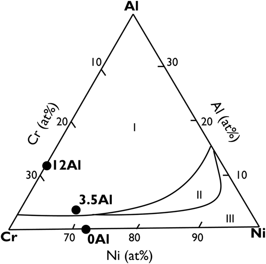
Film compositions were chosen based on the oxidation regimes predicted by Chen et al.Reference Chen and Lou7 with increasing amounts of Al at the expense of Ni in the base composition as shown in Fig. 1. The compositions were verified using Rutherford backscattering spectroscopy (RBS) with pure elemental film standards. Film thickness was controlled as a function of deposition time and was varied between 100 and 500 nm based on the characterization requirements. In addition to this, 1 at.% Y was added to two of the film compositions. The substrates used were 1 cm × 1 cm p-doped 〈100〉 orientation Si wafers with a 1 μm thermally grown SiO2 oxide.
Oxide maps overlaid on ternary composition diagrams for sputtered, nanograined NiCrAl films as adapted from Chen et al.Reference Chen and Lou7 Here, the oxidation regimes stand for (I) Al2O3, (II) Cr2O3 with internal oxidation, and (III) NiO with internal oxidation. Al2O3 is the preferred protective oxide followed by Cr2O3, and NiO is considered deleterious. Grain refinement leads to a larger compositional space for alumina formation.Reference Merz8 The circular black symbols represent sputtered film compositions, and are denoted by the aluminum concentration in the film.
To produce free-standing films for the oxidation heat treatments, poly(methyl methacrylate) (PMMA) was spun coat on the Si/SiO2 substrates at 500 rpm for 5 s followed by a 180 °C bake for 90 s. Films were then deposited on the PMMA, followed by the dissolution of PMMA using acetone to produce free-standing metallic films.
B. High-temperature oxidation and thermal stability
A thermogravimetric analyzer (TGA; Q50, TA Instruments, New Castle, Delaware) was used to determine the relative mass gain and oxide growth rate of the metallic films in nitrogen and air environments. Free-standing films were weighed out in roughly 3 mg batches and ramped from room temperature to 900 °C at a 10 °C/min ramp rate followed by a fast furnace quench.
A custom environmental control furnace equipped with an O2 gettering system was also used for shorter heat treatments on films that displayed the largest differences in their TGA behavior upon Y addition. The  ${{\rm{P}}_{{{\rm{O}}_{\rm{2}}}}}$ within the gettered argon measured at ambient temperature was between 10−12 and 10−14. The furnace was heated to 900 °C after which the samples were inserted into the hot zone in the low ${{\rm{P}}_{{{\rm{O}}_{\rm{2}}}}}$ environment using a push rod system for 5 or 15 min. This was followed by a rapid quench in an ice water cooled zone of the furnace in the same low ${{\rm{P}}_{{{\rm{O}}_{\rm{2}}}}}$ environment.
In situ transmission electron microscopy (TEM) heating of thin lamellae was conducted to deconvolute the effect of Y on the oxidation behavior and thermal stability of the NiCrAl films. Direct lift-out focused ion beam (FIB; Helios 600i, Thermo Fisher Scientific, Waltham, Massachusetts) samples of the films were prepared and mounted on Mo grids (Omni grids, Electron Microscopy Sciences, Hatfield, Pennsylvania). The thin lamellae were then heated in situ from room temperature to 900 °C at 10 °C/minute using a heat stage (Model 652, Gatan Inc., Pleasanton, California). Bright field TEM images and diffraction patterns were collected at every 50 °C interval, starting at room temperature and up to 900 °C.
C. Microstructural and chemical analyses
Cross-sectional TEM (JEM 2010 LaB6, JEOL, Ltd., Peabody, Massachusetts) samples of the as-deposited films were produced using FIB. Scanning (S) TEM and TEM samples of the oxidized films were lifted out for further analysis. Bright field TEM was used to determine the microstructure of the as-deposited films and oxidized films. STEM energy dispersive X-ray spectroscopy (EDS; JEM 2010F, JEOL, Ltd. and spherical aberration probe corrected Titan Themis Z with SuperX EDS detector, Thermo Fisher Scientific) was used to determine the chemical composition of the oxidized films.
Furthermore, photostimulated luminescence spectroscopy (PSLS; Horiba LabRam Aramis spectrometer, Horiba Ltd., Kyoto, Japan) was used to ascertain the polymorph of alumina formed on the aluminum containing oxidized films.Reference Tolpygo and Clarke32,Reference Stewart, Suzuki, Pollock and Levi33 A standard 10× lens and an incident laser of 633 nm with a spot size of 3 and a filter level of 0.6 was used to measure fluorescence peaks in the frequency range 13,992–14,843 cm−1.
III. RESULTS
A. Sputtered film compositions and starting microstructure
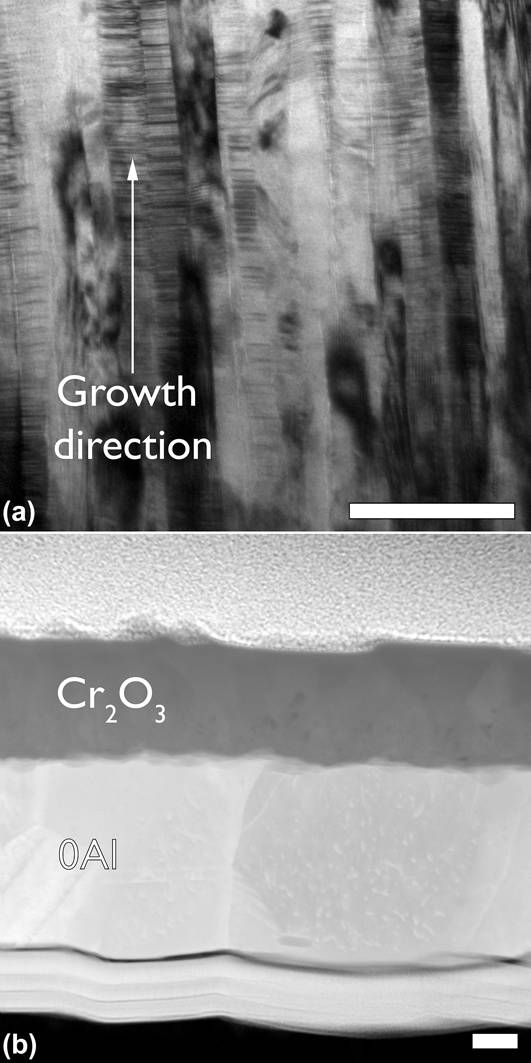
The sputtered film compositions that were verified using RBS are shown in Table I. The films have been identified based on their Al concentration and whether they contain Y. The 0Al and 0AlY films lie within the oxidation regime III, and the remaining films lie in oxidation regime I as shown in Fig. 1. Bright field TEM cross-sectional micrographs of the 0Al films revealed a characteristic columnar and nanograined microstructure with a grain width of 20 ± 1.7 nm and planar defects in the form of stacking faults as shown in Fig. 2(a). The film thickness was controlled as a function of deposition time and was roughly 500 nm for the oxidation tests. The films were determined to be chemically homogenous within the limits of the available characterization tools (TEM, EDS, and XRD).
Compositions of as-deposited NiCrAl–Y films determined by RBS.

(a) Bright field transmission electron micrograph of an as-deposited 0Al film, and (b) annular dark field scanning transmission electron micrograph of a N2 oxidized 0Al film. A low oxygen partial pressure allowed for the growth of a dense, and adherent Cr2O3. The films in all parts have been aligned with the growth direction from bottom to top. All scale bars are 100 nm.
B. Thermogravimetric oxidation in N2 and air
Results of the TGA oxidation test in N2 and air for the 0Al and 0AlY films are shown in Fig. 3(a). The temperature profile of the heat treatment is also overlaid on the plot. The origin of the time axis corresponds to the point at which any residual PMMA from the film lift-off step was burned off. This temperature was found to be roughly 350 °C. There was a clear difference in the slope, shape, and final normalized mass gain value for films that were oxidized in N2 versus in air. In both 0Al and 0AlY cases, the oxide growth rate and final mass gain was smaller in the N2 environment because of the lower  ${{\rm{P}}_{{{\rm{O}}_{\rm{2}}}}}$. Also, the films with the dilute Y addition show a slower oxide growth than their Y-free counterparts in both environments.
Thermogravimetric analysis data for (a) air and N2 oxidized 0Al and 0AlY films and, (b) air oxidized 0Al, 0AlY, 3.5Al, 12Al, and 12AlY films. N2 oxidation was less aggressive than air oxidation but made it difficult to discern the improvement from the Y addition. Air oxidation showed that Y addition improved the oxidation resistance of the films. The secondary vertical axis shows the temperature profile during the oxidation tests.
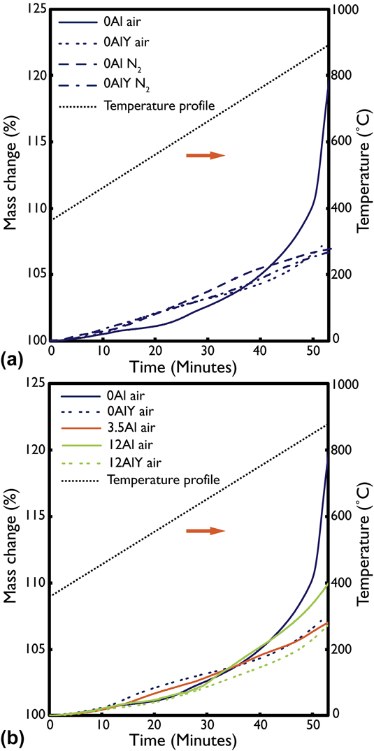
The lower  ${{\rm{P}}_{{{\rm{O}}_{\rm{2}}}}}$ N2 atmosphere formed slow-growing, dense oxides as shown in Fig. 2(b), while the air environment accelerated the oxidation and accentuated the differences in oxidation rates between the 0Al and 0AlY compositions. The TGA data for all five film compositions oxidized in air is plotted in Fig. 3(b). The final normalized mass gain was highest for the 0Al film and the lowest for the 12AlY film. By inspection of the shape and trajectory of the mass gain profiles, the final oxide growth rate appears the highest for the 0Al film and the lowest for the 3.5Al film.
Table II lists the measured values of final normalized mass gains and final oxide growth rates estimated from the TGA data. The final normalized mass gain is determined by the final value of the mass change after ramping to 900 °C in air. The final oxide growth rate was estimated by the slope of the TGA curve during the final 10 °C ramp from 890 to 900 °C. All oxidized films eventually either formed an external Al or Cr oxide. The oxide thickness for films oxidized in the TGA were measured via TEM analysis and are also reported in Table II. Comparing the data extracted from the TGA analysis to direct measurements of oxide thickness, it becomes apparent that the TGA cannot be used to rigorously predict oxide thickness. However, these data remain valuable to qualitatively compare the oxidation behavior of films with large differences in their normalized mass change and final oxide growth rate.
Mass change and oxide growth rate extracted from TGA analysis; oxide chemistry and oxide thickness measured from TEM analysis for films oxidized in air.

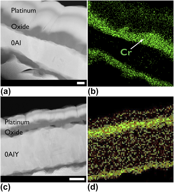
The STEM micrographs of representative group III and group I films with an EDS map chemical overlay are shown in Fig. 4 and Figs. 5(a)–5(d). Note that the 0Al and 0AlY films formed an external chromia as expected for a group III composition shown in Fig. 1. The results of the PSLS data collected on the three alumina forming films to confirm the polymorph are shown in Fig. 5(e). In all three cases, the α-Al2O3 doublet centered at 14,400 cm−1 was detected.
Annular dark field scanning transmission electron micrographs of air oxidized (a and b) 0Al, and (c and d) 0AlY films and the energy dispersive X-ray spectrometer chemical map of the metal present in the oxide. Scale bars for parts (a) and (b) are identical, and scale bars for parts (c) and (d) are identical. All scale bars are 100 nm. The 0AlY films displayed a slower oxide growth rate as evidenced by the thinner oxide, and Cr remaining in the film interior.
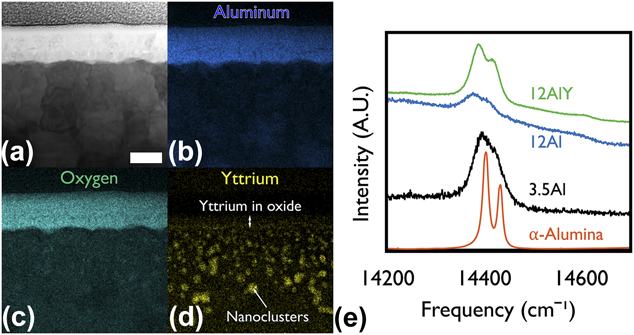
(a) Bright field scanning transmission electron micrograph of an air oxidized 12AlY film. High resolution energy dispersive X-ray spectrometer chemical maps of (b) Al, (c) O, and (d) Y. No internal oxidation of Y was observed. Yttrium was incorporated in the oxide, mostly at the oxide-film interface. Yttrium also formed nanoclusters in the film. The films in all parts have been aligned with the growth direction from bottom to top. All images have identical scale bars equal to 100 nm shown in part (a). (e) Photostimulated luminescence spectrum of air oxidized Al containing films against an α-alumina standard. All the air oxidized Al containing films were confirmed to have grown α-alumina based on the characteristic doublet measured.
C. Ex situ oxidation in low  ${{\bf{P}}_{{{\bf{O}}_{\bf{2}}}}}$ conditions

The substantial difference in oxide growth rate between the 0Al and 0AlY compositions as extracted from the TGA analysis motivated additional ex situ oxidation treatments. Bright field TEM micrographs of 0Al and 0AlY films after 5 and 15 min of oxidation at 900 °C in low  ${{\rm{P}}_{{{\rm{O}}_{\rm{2}}}}}$ conditions in an environmental furnace are shown in Figs. 6(a)–6(d). Remnants of the initial columnar microstructure are evident in the 0AlY films suggesting a slower microstructural evolution compared to the 0Al film. In addition to visual differences in the microstructure, electron diffraction patterns with the same selected area aperture shown in the insets of Figs. 6(a) and 6(c) provide further evidence of the finer grain structure for the 0AlY films. The diffraction pattern for 0AlY consisted of rings, suggesting the presence of several grains in contrast to a nearly single grain diffraction pattern for the 0Al films.
Bright field transmission electron micrographs of (a and b) 0Al, and (c and d) 0AlY films after (a and c) 5 min and (b and d) 15 min of oxidation under low oxygen partial pressure at 900 °C. The films containing Y displayed a higher tolerance to microstructural evolution and slower oxidation rate. The insets in (a), and (c) show selected area electron diffraction patterns for the corresponding samples indexed according to an FCC Ni-solid solution. Some original grains were observed in the 0AlY sample after 5 and 15 min of oxidation. (e and f) Annular dark field (ADF) scanning transmission electron micrographs of the 15 min oxidized 0AlY film. Oxide nuclei are seen as opposed to a discontinuous external scale in the case of the 0Al film. Y nanoclusters were also seen near free surfaces. The films in all parts have been aligned with the growth direction from bottom to top. All scale bars are 100 nm.
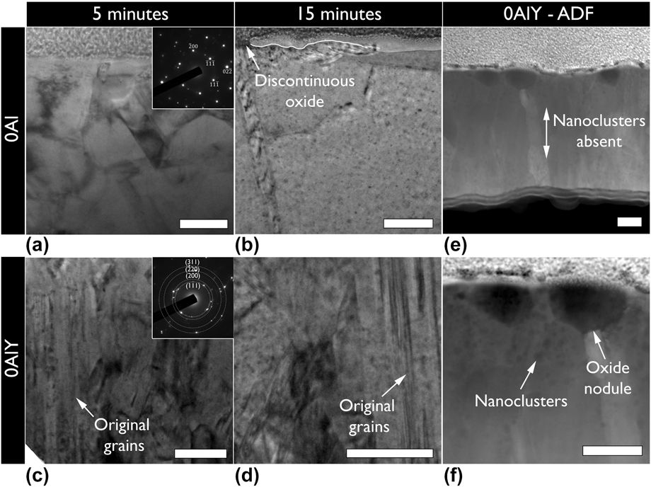
The oxidation behavior of the 0Al and 0AlY films were also different. Unlike, the 0Al films where a discontinuous oxide scale was observed as shown in Fig. 6(b) (the oxide/film interface has been partially delimited by a white line for clarity), the 0AlY films displayed individual oxide nuclei as shown in Figs. 6(e) and 6(f). The chemistry of the oxide nuclei (EDS point measurement: 3.6 ± 0.5 at.% Ni, 67.6 ± 1.9 at.% Cr, 9.4 ± 1.3 at.% Y, 19.4 ± 1.1 at.% OFootnote a) was found to be chromium-rich with incorporated Y. The 0AlY films displayed the formation of Y-rich nanoclusters near the oxidized surface as confirmed in Fig. 6(f) and using EDS point measurements (64.5 ± 1.5 at.% Ni, 24.8 ± 0.8 at.% Cr, 10.7 ± 1.0 at.% Y). Such Y clustering and surface segregation was also observed in TGA samples oxidized for longer times in air as shown in Fig. 5(d).
D. In situ heating
The 12Al and 12AlY compositions were selected for in situ TEM heating experiments based on the PSLS confirmation of α-Al2O3. The in situ TEM heating results comparing the thermal stability in 12Al and 12AlY lamellae under low  ${{\rm{P}}_{{{\rm{O}}_{\rm{2}}}}}$ conditions are shown in Fig. 7. The microstructural evolution in a 12Al lamella and 12AlY lamellae is shown in Figs. 7(a)–7(h). The 12AlY lamella showed a different initial texture compared to 12Al as can be seen in Figs. 7(e) and 7(a), respectively. The initial grain size in the 12AlY lamella also appeared finer than the 12Al lamella. Upon thermal activation, the 12Al lamella began to recrystallize around 650 °C as shown in Fig. 7(b). In comparison to this 12AlY lamella began to recrystallize around 750 °C as shown in Fig. 7(g).
In situ transmission electron microscope heat treated (a–d) 12Al, and (e–h) 12AlY lamellae. The heat treatment temperatures shown for both samples are (a and e) 100 °C, (b and f) 650 °C, (c and g) 750 °C, and (d and h) 900 °C. The inset of each part is the corresponding selected area electron diffraction pattern. The initial microstructure of the 12AlY lamella had a different texture and finer grain size compared to the 12Al lamella. Upon thermal activation, the 12AlY lamella showed a higher tolerance to recrystallization and grain growth because of grain boundary pinning by Y nanoclusters. The lamellae in all parts have been aligned with the growth direction from bottom to top. All scale bars are 100 nm.
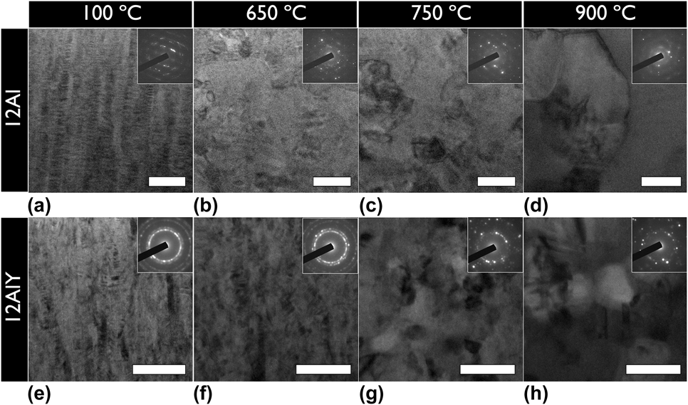
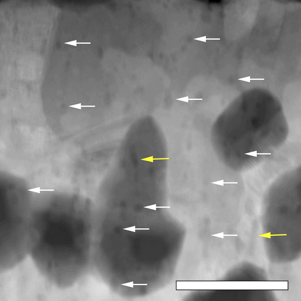
Yttrium clustering in the 12AlY lamella first became evident at 650 °C, shortly before the recrystallization event. Figure 8 shows the distribution of the Y nanoclusters in the 12AlY film after the in situ heat treatment. Most clusters appeared to be distributed homogeneously and were spherical in shape. However, in some cases, clusters were observed to be elongated along the same direction as the original grain boundaries. On comparing the final grain size in the 12Al as shown in Fig. 7(d) and 12AlY films shown in Fig. 7(h), it is evident that the 12AlY films displayed less grain growth.
Annular dark field scanning transmission electron micrograph of the in situ heat treated 12AlY lamella after exposure to 900 °C. Yttrium nanoclusters were found to be distributed homogeneously throughout the lamella. In most cases, the nanoclusters appeared spherical as shown by the white arrows. In some cases, elongated precipitates were seen, presumably along the original grain boundaries as shown by the yellow arrows. The grains with darker contrast were found to be rich in Cr, this artifact is attributed to the diffusion of Pt from the protective layer into the matrix which seems to reduce the solubility of Cr in Ni. The scale bar is 100 nm.
IV. DISCUSSION
The morphology and durability of an oxide may be determined within the first few minutes of exposure to an oxidizing environment. Development or suppression of fast-growing, lower density, and mechanically compromised oxides may mean the difference between a spallation-prone, consuming oxide scale and an adherent, protective oxide. Based on the insight provided by this study and the extensive body of the oxidation literature, three clear routes to controlling transient oxidation behavior emerge: (i) increasing the concentration of oxygen-active alloying elements such as Al or Cr, (ii) accelerating diffusion of Al or Cr toward the solid/gas interface, or (iii) allowing additional time for diffusion of Al or Cr to the solid/gas interface. All three of these avenues are observed in this study. The discussion below attempts to deconvolute the contributions of each, with specific emphasis on the latter two.
A. Effect of initial microstructure
The link between fine grain size and oxidation has been studied previously for the NiCrAl alloy system.Reference Liu, Gao, Dahm and Wang34 A higher grain boundary density has been reported to improve the selective oxidation of desirable species and improve oxide adherence because of the closely spaced surface features. The alumina forming compositional space (group I) shown in Fig. 1 for sputtered nanograined alloysReference Chen and Lou7 is larger than that for the microcrystalline counterpart reported in previous studies.Reference Wallwork12 This phenomenon is postulated to occur because of the high grain boundary density that favors faster grain boundary diffusion and the large number of oxide nucleation sites in the sputtered microstructure.Reference Gleiter35
On comparing the expected oxide chemistry in Fig. 1 to the results from this study in Table II, it is evident that the 0Al and 0AlY films are not consistent with expectations. In both cases, Cr2O3 formed externally in place of the expected NiO with internal oxidation. Since the film compositions were chosen based on empirically extrapolated data presented in Fig. 1, such deviations are not unreasonable.
However, this inconsistency in oxidation behavior is not the only deviation from expected behavior observed in this study. An Al to Cr ratio of at least 0.25 is required in bulk coarse grained alloys to form alumina.Reference Rupert27 And, in air, α-alumina usually forms at temperatures above 1000 °C.Reference Yang, Schumann, Levin and Rühle19,Reference Grabke20 Yet, in the 3.5Al films, an external α-alumina scale was formed (Al to Cr ratio ∼0.14) well below the micrograined ratio with a maximum temperature exposure of 900 °C. It is hypothesized that the sputtered microstructure provides rapid diffusion pathways along the columnar grain boundaries for oxygen-active solutes like Al and Cr that would otherwise be suppressed at such low temperatures. The enhanced surface concentration of Al and Cr allows for the development of protective, slow-growing alumina and chromia, which reduce the oxygen activity and inhibit the formation of deleterious fast-growing NiO and spinels.Reference Giggins and Pettit13
B. Effect of oxygen partial pressure
Instead of providing routes for accelerated diffusion of oxygen-active solutes, a low  ${{\rm{P}}_{{{\rm{O}}_{\rm{2}}}}}$ environment slows down the rate at which oxygen is delivered to the solid–gas interface. This in turn provides more time for oxygen-active solutes like Al and Cr to diffuse to the surface. Since desirable species like Al and Cr require a lower oxygen activity to form an oxide, such conditions favor their growth over deleterious NiO and spinels. Low ${{\rm{P}}_{{{\rm{O}}_{\rm{2}}}}}$ can also suppress the growth of metastable aluminas and improve high temperature stability of the oxide.Reference Chraska, Dubsky, Neufuss and Pisacka23,Reference Clark24
Consider the data presented in Figs. 2(b), 3(a), and 4(a) for the 0Al films. Not only is the normalized mass gain for the “0Al N2” an order of magnitude lower than “0Al air”, but the morphology of the resulting oxides is strikingly different. A continuous, dense chromia scale is observed in Fig. 2(b) relative to the spiky morphology found on the same films oxidized in air in Fig. 4(a). Moreover, several instances of oxide spallation were observed following oxidation of 0Al specimens in air.
Investigation of the transient oxidation behavior under low  ${{\rm{P}}_{{{\rm{O}}_{\rm{2}}}}}$ provided additional insight on the morphological differences observed in Figs. 2(b) and 4(a). The 0Al films rapidly (<15 min) grew an interrupted, otherwise uniform, external oxide [see Fig. 6(b)] under low ${{\rm{P}}_{{{\rm{O}}_{\rm{2}}}}}$ conditions. A parallel, short-term air oxidation experiment could not be performed. However, it is straightforward to conclude that the oxide morphology observed in Fig. 6(b) is the precursor to the continuous, protective oxide observed in Fig. 2(b) and is also consistent with the morphology of the Y-containing compositions oxidized in air in Figs. 4(c) and 4(d).
C. Effect of Y on oxidation behavior
The role of Y in the oxidation of sputtered, nanograined thin films is more complicated. REs like Y are commonly associated with the selective oxidation of desirable species like Al and Cr. In RE ion implanted alloysReference Hou and Stringer36 and RE oxide dispersion strengthened alloys,Reference Pint, Leibowitz and DeVan37 this effect was credited to the refinement of grain size which enhanced the diffusivity of desirable species. Many other studies have reported a RE effect involving slower growth of alumina,Reference Pint and Alexander38,Reference Pint, Martin and Hobbs39 and chromiaReference Hou and Stringer36,Reference Cotell, Yurek, Hussey, Mitchell and Graham40,Reference Chevalier41 via suppressed transport through the oxide itself. It is not clear from the existing literature which of these mechanisms are more effective or if they may be synergistic.
The addition of Y to the 0Al and 12Al films measurably decreases the oxide growth rate, as observed from the TGA data presented in Fig. 3. The observed decrease for the 12AlY samples may be within the error of the measurement; however, this effect is more pronounced in the 0Al films as the oxide growth rate in 0AlY was lower by an order of magnitude. The magnitude of this effect was similar to that observed for the 0Al film oxidized in air and in N2—albeit, due to different mechanisms. As already discussed in Sec. IV.B., oxidation under low  ${{\rm{P}}_{{{\rm{O}}_{\rm{2}}}}}$ conditions allows more time for diffusion of Al or Cr to the oxidation front. By contrast, based on evidence presented in Figs. 5 and 6, Y stabilizes accelerated diffusion pathways during the earliest stages of oxidation, thus facilitating rapid transport of Al or Cr to the solid/gas interface.
Observation of Y nanoclusters after oxidation in both low  ${{\rm{P}}_{{{\rm{O}}_{\rm{2}}}}}$ [see Figs. 6(e) and 6(f)] and air [see Fig. 5(d)] environments is consistent with calculations that suggest a highly positive segregation enthalpy of Y in nanocrystalline Ni.Reference Murdoch and Schuh42 Previous studies have attributed similar nanoclusters to improve microstructural stability through a Zener pinning mechanism by hindering grain boundary motion.Reference Darling, Rajagopalan, Komarasamy, Bhatia, Hornbuckle, Mishra and Solanki26 Minor amounts of Y, therefore, enable more efficient implementation of the mechanisms described in Sec. IV.A.
However, these observations cannot be fully decoupled from more subtle chemical effects. Yttrium is unambiguously incorporated in the transient chromia nuclei after 15 min of oxidation, verified using EDS point measurements as described in Sec. III.C. Such incorporation is also shown for a fully formed Al oxide in Figs. 5(b)–5(d). Careful inspection of the PSLS data [see Fig. 5(e)] reveals that the α-alumina doublet is best defined for the 12AlY film. The surprising observation of α-alumina at such low temperatures, and in the case of 3.5Al, such low Al concentration, has already been discussed. Yet, comparison of the spectra suggest that the nucleation and quality of the desired alumina phase may be further influenced by incorporation of Y.
D. Effect of Y on thermal stability
The available data are insufficient to rigorously deconvolute the two proposed roles of Y during the transient stages of oxidation. However, the thermal stability of the Y-containing microstructures may be probed independently by removing the driving force for oxidation, thereby providing some additional insight on the underlying mechanisms common to both experiments.
In situ TEM heating experiments revealed that dilute Y addition to the 12Al lamella changes the initial texture and reduces the grain size as shown in Figs. 7(a) and 7(e). Yttrium also seemingly improves the thermal stability of the 12AlY lamella by forming nanoclusters that pin the grain boundaries and delay the onset of recrystallization from around 650 °C to around 750 °C. After the recrystallization event in 12AlY, the nanoclusters limit the growth of the newly formed grains as evidenced from the difference in final grain size between the 12Al and 12AlY films [see Figs. 7(d) and 7(h)]. Delayed initialization of recrystallization and reduced grain growth rates due to strong, local pinning forces have been reported for other systems.Reference Kwon and DeArdo43
Comparing the oxidation and in situ heating observations suggests that even modest stabilization of the initial nanocrystalline microstructure, and the associated fast diffusion pathways, is sufficient to dramatically alter the oxidation behavior. It is also worth noting the differences in Y nanocluster distribution. The Y nanoclusters are evenly distributed across the lamella thickness during the in situ heat treatments (see Fig. 8), whereas a denuded zone is apparent in the middle of the film thickness when the nanoclusters form under oxidizing conditions [see Fig. 6(e)]. The Y nanoclusters do not appear to oxidize internally and have a similar size distribution relative to those in the unoxidized sample. One may postulate that the differences in nanocluster distribution may be associated with the observed uptake of Y in the oxide nodules, eventually being completely consumed by the oxide. However, the nanoclusters are absent in the center of the film very early on and remain seemingly stable as the oxide fully develops—see Fig. 6(f) versus Fig. 5(d).
Although a comprehensive description of the Y contribution remains elusive, the results and analysis presented here emphasize the importance of the transient stages of oxidation and several avenues for the manipulation thereof.
V. CONCLUSIONS
In this study, routes to control the early stages of oxidation to grow dense, protective oxides in the sputtered NiCrAl system have been discussed. The role of the columnar, nanograined microstructure is found to be crucial to the rapid diffusion of desirable oxygen-active species like aluminum and chromium. Such rapid diffusion allowed the development of slow-growing alumina and chromia, which establish a lower oxygen activity and inhibit the growth of deleterious, fast-growing oxides. Limiting the oxygen partial pressure during oxidation provided an alternate route to promote the oxidation of aluminum and chromium. In addition to a desirable oxide chemistry, the oxide morphology and adherence also improved by limiting the oxygen partial pressure.
Dilute yttrium additions to sputtered NiCrAl films showed beneficial effects on both the oxidation resistance and thermal stability of the films. Yttrium was shown to measurably slow down the oxidation rate, similar in magnitude to the improvement seen by reducing the oxygen partial pressure. However, the mechanism behind this improvement was more complicated. The nanoclustering of Y under thermal activation improved the microstructural stability of the sputtered films. By temporarily stabilizing the original grain boundary network, aluminum and chromium diffusion was accelerated toward the oxidation front, thus enabling the establishment of preferred slow growing oxide polymorphs even at lower temperatures. Understanding the transport of solutes through nonequilibrium microstructures and how this transport affects the transient stages of oxidation can pave the way for new oxidation mitigation strategies in structural alloys.
ACKNOWLEDGMENTS
The authors would like to thank the Frederick Seitz Materials Research Lab for providing the facilities to conduct most of the experiments. Many thanks to Dr. Pinshane Y. Huang at the University of Illinois for facilitating the high-resolution EDS maps at ThermoFisher Scientific. The authors would also like to thank Colin A. Stewart and Carlos G. Levi at University of California-Santa Barbara for performing the PSLS measurements. This project was supported by the Department of Materials Science and Engineering at the University of Illinois, Urbana-Champaign.


 Open access