

Introduction
Nowadays, GaN technology is highly adopted by the industry and its benefits and drawbacks are well known in comparison with the alternative of GaAs [Reference Komiak1, Reference Campbell, Balistreri, Kao, Dumka and Hitt2]. Among its advantages, we can highlight the wideband output power performance, high breakdown voltage, and high current density. These electrical characteristics combined with the thermal conductivity of SiC make this technology well positioned to substitute the existing TWTAs on broadband communications and electronic warfare.
The main design topologies for high-power amplifiers (HPA) are the distributed power amplifiers (DPA), or its variant non-uniform distributed power amplifiers (NDPA), and the corporate power amplifier. The latter one is subject to the classic Bode-Fano limitation for reactive matching [Reference Fano3] but it can obtain more gain and, generally, more power than (N)DPA [Reference Campbell, Balistreri, Kao, Dumka and Hitt2, Reference Ghavidel, Tamjid, Fathy and Kheirdoost4]. Its drawbacks are poor reflection coefficients, less bandwidth, and, generally, higher current consumption and more heat to dissipate.
Some semiconductor companies have GaN HPA solutions over the 6–18 GHz band and several articles about reactively matched HPAs have been published up to date [Reference Barisich, Gebara, Gu, Storey, Aflaki and Papapolymerou5–Reference Jeong, Jang, Shin, Yom, Kim, Lee and Lee12]. Nevertheless, most of them are manufactured outside Europe. This condition could lead to restrictions on their use and this dependency from third-party countries could impact on system designs and create export issues for European products. A possible strategy to mitigate these problems for a system design company is to create its own portfolio regarding critical components. Due to the previous considerations, this design was developed on GaN technology using a 0.25 µm gate length process from UMS, GH25.
Moreover, the design presented in this article outperforms the European designs referred in the previous paragraph. The MMIC presented on [Reference Dennler, Quay and Ambacher9] has less output power and power added efficiency (PAE) [Reference Gonzalez-Garrido, Grajal, Cubilla, Cetronio, Lanzieri and Uren7, Reference Gonzalez-Garrido, Grajal, Cetronio and Marescialli8], have similar characteristics but operating in a 2–6 GHz band, and, finally [Reference Mouginot, Ouarch, Lefebvre, Heckmann, Lhortolary, Baglieri, Floriot, Camiade, Blanck, Le Pipec, Mesnager and Le Helleye6, Reference Schmid, Sledzik, Schuh, Schroth, Oppermann, Brückner, van Raay, Quay and Seelmann-Eggebert10, Reference Dennler, Maroldt, Quay and Ambacher11], achieve similar characteristics using an additional amplification stage. Those assertions are detailed in Table 1.
Comparison among the different works referenced

Therefore, this paper presents the development and characterization of an ultra-wideband 6–18 GHz HPA on 0.25 µm GaN on SiC process from UMS. It is organized as follows. Section ‘Corporate amplifier design’ describes the design procedure, topology, biasing, matching networks design, and stability analysis. Section ‘Assembly’ presents thermal and assembly considerations. Section ‘Measurements’ lists the results obtained in measurements on wafer and on jig and the comparison with simulations carried out during the design stage. Finally, Section ‘Conclusions’ shows the conclusions of this article.
Corporate amplifier design
The design requirements proposed for this HPA are a full operating bandwidth from 6 to 18 GHz. The HPA should be capable to deliver an output power between 5 and 10 W with a PAE >15% with a target of 20%. Gain at saturation should be more than 7 dB.
Amplifier topology and biasing
The corporate topology was selected for the design of this amplifier. In this topology, the maximum output power is defined by the last amplifier stage. Two stages are enough to achieve the amplifier requirements. In this case, four different options were studied to define the output amplification stage: four transistors with eight fingers, four transistors with six fingers, and eight transistors with eight and six fingers. The power density of the GaN process used is 4.5 W/mm; therefore, an output power of 10 W, considering insertion losses of 1.5 dB for the output matching network, gives a minimum total gate periphery of 3.15 mm. This periphery was used to define the gate width for each transistor evaluated for the output stage, given 130 and 100 µm gate width using four transistors of six and eight fingers, respectively, and a half of these values if eight transistors were selected. As gate width increases, more output power is achievable, but transistor output capacitance increases as well. It is easier to generate more gain and power using one additional stage and doubling the number of transistors involved maintaining the gate periphery. In this design, a minimum number of matching networks was preferred because larger gate width implies more difficult impedance matching. On the other hand, fewer transistors per stage lead to easier combination or division networks. Considering the previous discussion, four transistors were selected for the output stage. The first stage is composed of two transistors with 8 × 70 µm gate fingers, while the second stage is composed of four transistors with 8 × 100 µm gate fingers. A schematic representation of the amplifier can be seen in Fig. 1.
Schematic representation of the amplifier designed.

For the input stage, transistors shall be capable to deliver enough power to saturate the output transistors in order to maximize the output power and PAE, and enough gain to compensate the losses of the first two impedance matching networks. The gate periphery necessary for these transistors was selected supposing a maximum loss of 5 dB at 18 GHz for the input and inter-stage matching networks. The maximum output power of each transistor of the first stage is 34 dBm.
The bias point of the transistors was selected for deep class AB trying to improve efficiency. The foundry gives its own recommendations regarding the drain current density. In this process, the recommended drain current density was around 100 mA/mm. DC simulations were carried out varying the drain and gate voltage to obtain the characteristic I–V curves of each transistor and calculate the corresponding current density. Drain voltage was fixed at 30 V, while the gate voltage was obtained by simulations and was fixed at −3.1 V with a total drain current of 580 mA.
Impedance matching networks design
There are three different matching networks in this amplifier. Each network has been treated as a filter design problem. Combination or division N-port networks were first converted into two-port networks and then, a Chebyshev impedance transformer filter design technique was applied [Reference de Hek13, Reference Matthaei14].
Input and output impedances of the transistors were evaluated by load pull simulations carried out with ADS from Keysight. Load impedance circles for constant output power and PAE were obtained. These circles describe the load impedances for a transistor in which it is capable to deliver a specific power or obtain an efficiency level at different frequencies. The transistors used in this power amplifier have load impedances for maximum output power and maximum PAE close together. This characteristic allows an easier design of the impedance matching networks due to one load impedance for one specific frequency can be good enough to achieve a good performance tradeoff.
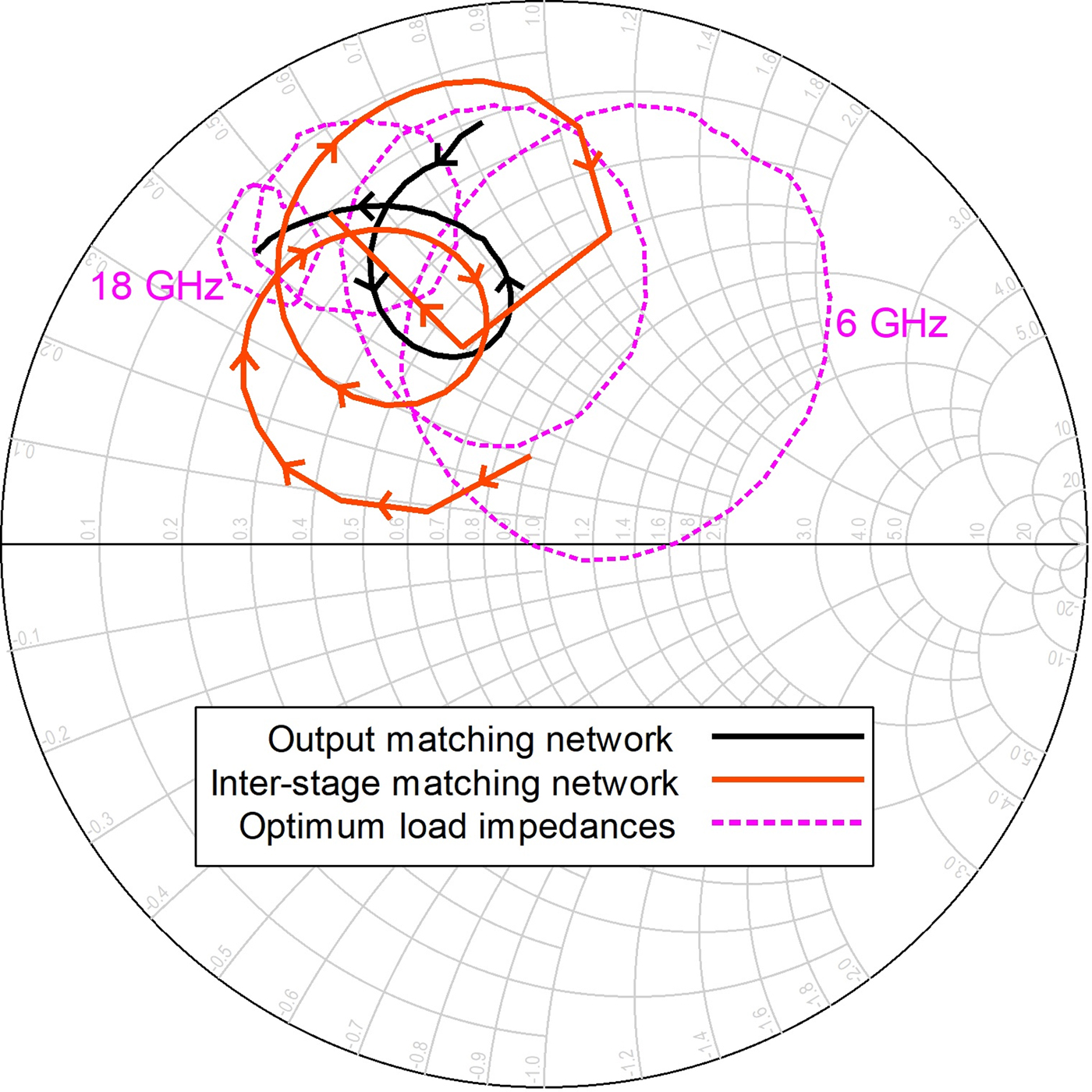
A group of constant output power circles was defined for frequencies between 6 and 18 GHz in 2 GHz steps. These circles were different regarding the output power that the transistor will be capable to deliver at one frequency. At 6 GHz, a circle was defined for an output power 1.5 dB less than the maximum achievable at this frequency, while at 18 GHz, the circle was defined for an output power 0.5 dB less than its maximum. The circles defined were tighter accordingly as the frequency increases. The reason for this selection is the own transistor capabilities, because as it is well known that a transistor delivers more power at low frequencies than at high frequencies. The use of these contours allows the designer to select properly the impedances of the matching networks given an additional degree of freedom and make possible the quick identification of the quality of the impedance synthesized for a certain frequency. In Fig. 2, such circles are depicted from 6 to 18 GHz.
Designed impedances for the output and inter-stage matching networks on 6–18 GHz (solid line). Transistor load impedance circles of constant output power at 6, 10, 14, and 18 GHz (dotted line).
In the corporate amplifier design, the design flow of the networks is backwards, starting with the output matching network. This network has four input ports, the transistor's drains, and one output port, the amplifier's output. It was converted into a two-port network with a source impedance Z S = R + jX and a load impedance Z L = 50 Ω, where Z S is the conjugated optimum load impedance of the output transistors for maximum output power, as defined in the previous paragraph. Following the procedure described in [Reference de Hek13], the output matching network was designed. The influence of the output drain capacitance, C ds, is compensated with a parallel inductance close to the outputs of the transistors. Depending on the impedance transformation ratio, the bandwidth and maximum loss of this network, an order for the filter shall be selected following the tables calculated on [Reference Matthaei14]. The theoretical lumped elements obtained in the Chebyshev filter design are synthesized using ideal microstrip transmission line elements and later, transformed into real transmission lines. Finally, these microstrip elements are slightly optimized to fulfill the insertion loss and characteristic impedance criteria over the whole bandwidth.
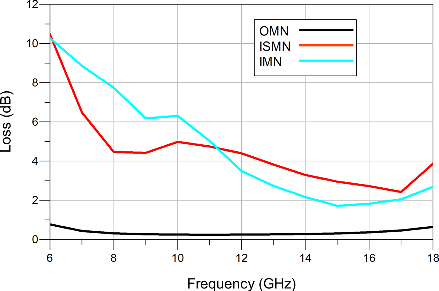
Input and inter-stage matching network design procedure was similar to the presented above. For the inter-stage network, the source impedance is the conjugated optimum load impedance for the first-stage transistors, while the load impedance is the conjugated input impedance of the second-stage transistors. The input matching network design is similar to the developed for the output network. Figure 2 shows the synthesized impedances for the output and inter-stage matching networks from 6 to 18 GHz. It can be seen that these networks were designed attending their performance at high frequency because their impedance at high frequency is closer to the appropriate described by the impedance contours obtained. In order to simplify the figure, only constant output power contours for the output stage are depicted but are similar to the input stage contours. The insertion loss of the three designed networks is depicted in Fig. 3. Note that the power division loss is not considered. Note also the necessary equalization at low frequencies in order to obtain a flat response compensating the gain slope of the transistors.
Simulated insertion loss of the three designed impedance matching networks.
Stability analysis
One of the major issues of corporate power amplifiers is stability. The own transistors could be unstable, the structure can form feedback loops and there may be odd mode oscillations. To ensure an unconditionally stable amplifier, small and large signal stability analysis was performed.
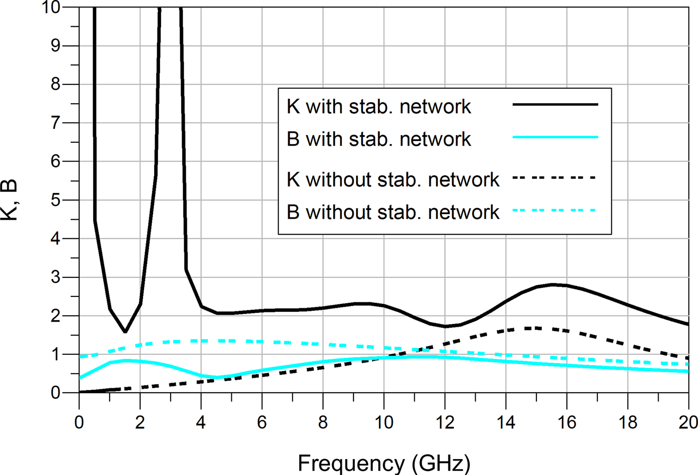
Small signal stability involves S-parameter analysis using the Rollet's factor criterion. Without a stabilization network, the transistors used in this design are unconditionally stable only between 10 and 20 GHz, where K > 1 and B > 0, as shown in Fig. 4. Series RC stabilization networks in combination with RLC gate bias network were designed. One of such networks is shown in Fig. 5(a). The resulted values of these components are indicated in Table 2.
Small signal stability factors for the output stage transistor with (solid line) and without (dotted line) the stabilization network.
(a) Stabilization network with series RC and parallel RLC bias network. (b) Odd mode stabilization resistors between adjacent transistors.
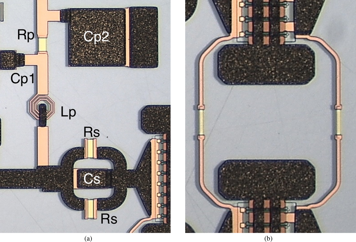
Component values for the stabilization networks

More detailed analysis was carried out to study the large signal stability, using a pole-zero technique detailed in [Reference Suarez, Jeon and Rutledge15, Reference Anakabe, Collantes, Portilla, Jugo, Mons, Mallet and Lapierre16].
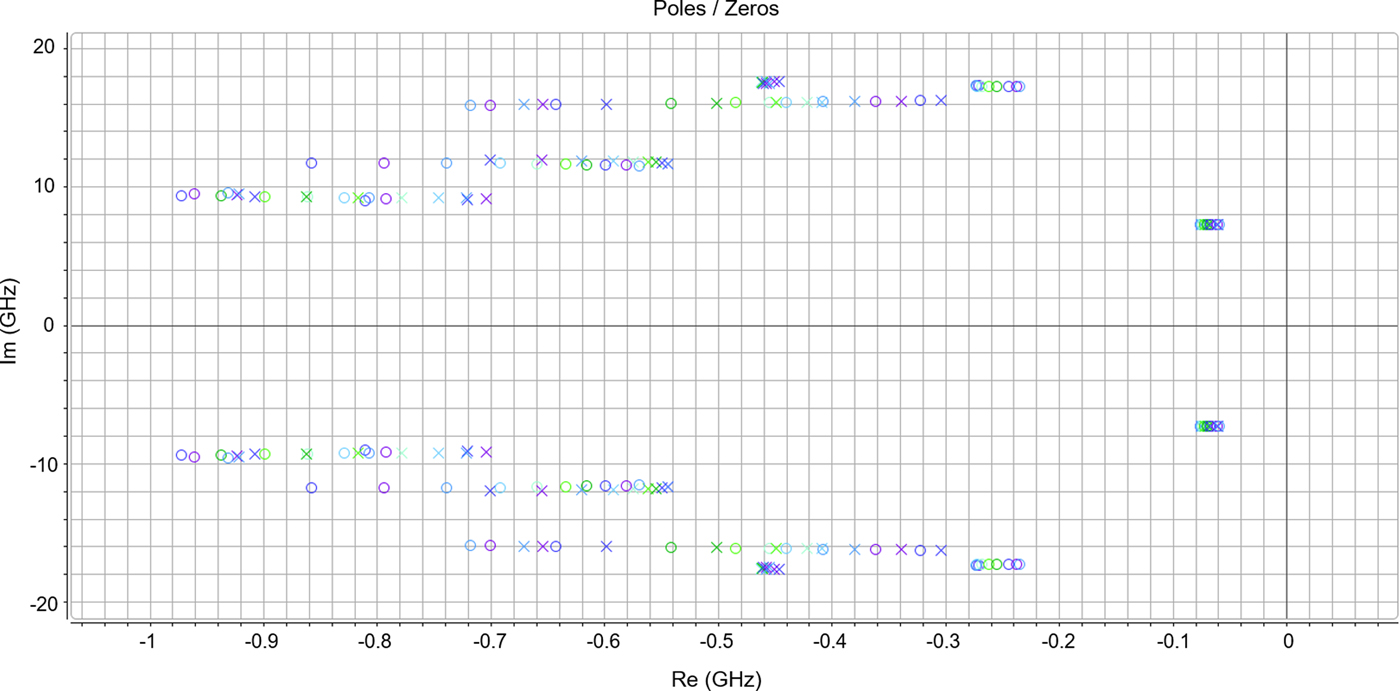
Simulations were carried out using the templates for Keysight ADS available with STAN software utility from IV-CAD [17, 18]. The whole amplifier is configured to work in a permanent large signal state, while a small signal perturbation is injected in a particular node of the amplifier. This simulation produces a transfer function that is exported and analyzed with STAN. The amplifier is unconditionally stable if there are no poles with a real positive part. If there are any poles with a positive real part, the amplifier may oscillate at the frequency indicated by this pole. Furthermore, to be sure of the amplifier stability, several simulations have to be carried out. It is mandatory to repeat the analysis dividing the whole frequency band into smaller sub-bands, changing the perturbation input node and varying some design variables such as gate voltage. In Fig. 6, the result of a stability analysis sweeping the gate voltage is depicted. In this figure, it is shown that the poles move toward the positive real axis, but never cross it. The sweeping was configured from −4.3 to −2.5 V to ensure that the amplifier goes from pinch off to beyond the quiescent point defined.
Pole-zero analysis result for a gate voltage sweeping. No unstable poles observed.
Neither loop nor odd mode oscillations were detected in the analyses performed. Nevertheless, 100 Ω resistors were placed connecting the pairs of gates or drains of adjacent transistors to avoid odd mode oscillation. A detail of these resistors can be seen in Fig. 5(b).
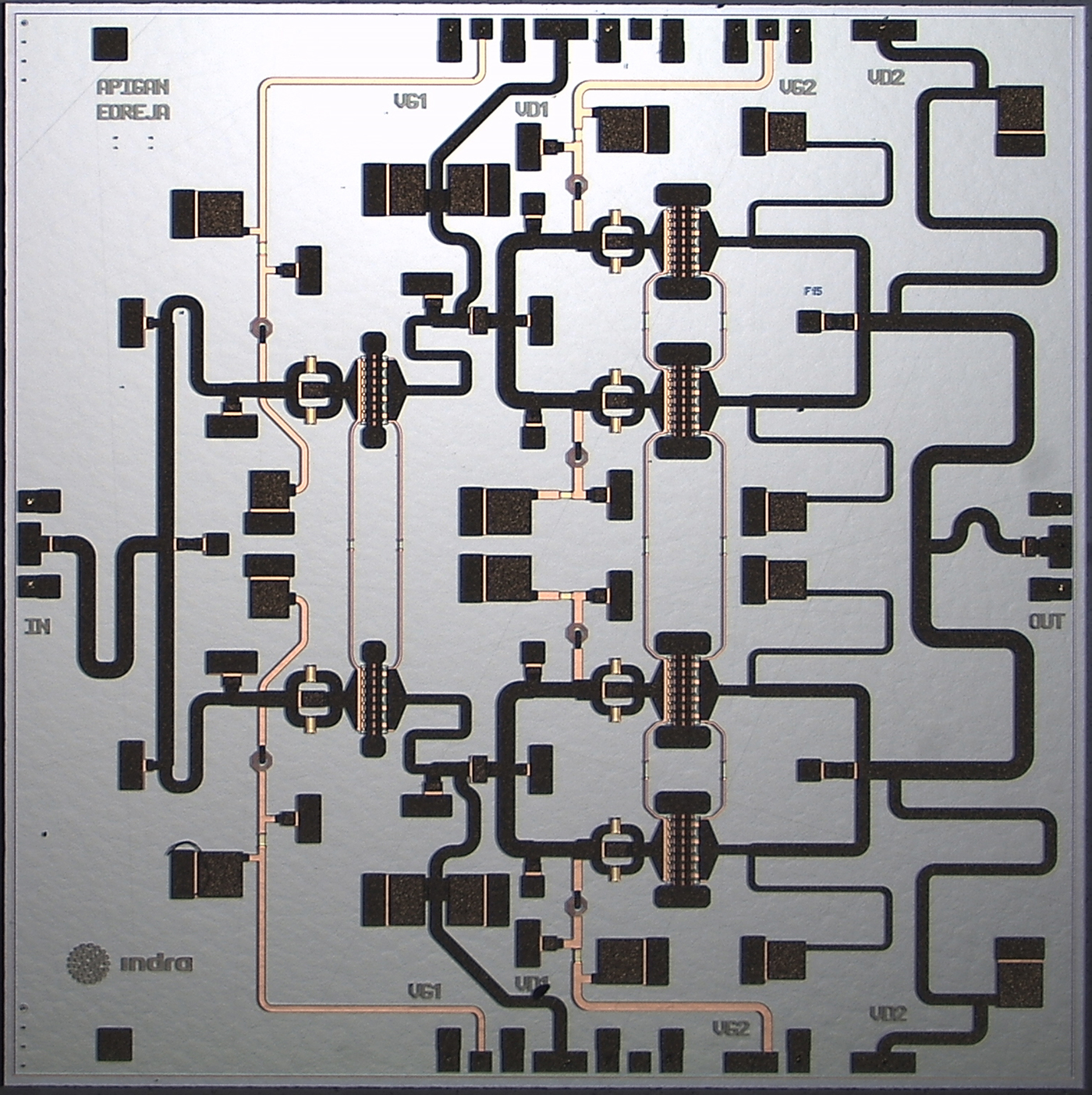
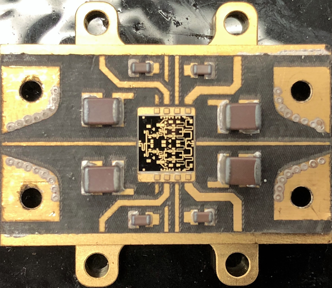
After the design steps described in the previous sections, a photograph of the final amplifier designed is shown in Fig. 7 with a size of 5 × 5 mm.
Die photograph of the GaN power amplifier designed.
Assembly
A CuW jig was fabricated for testing this HPA. This metal composite is W75/Cu25 and has a thermal conductivity of 190 W/(m·K) and better material matching to SiC than aluminum (CTE of 24 × 10−6/°C) due to its CTE of 9.7 × 10⁻⁶/°C, more similar to the SiC (4 × 10⁻⁶/°C). Three different attachment methods were discussed: a Gold Tin preform for eutectic soldering, a Gold Tin solder paste, and a high thermal conductivity epoxy. The first two options consist of an alloy with a composition of 80Au20Sn, which requires a high-temperature soldering process (around 280°C) while the epoxy needs a lower temperature to cure (near 200°C) [19]. The epoxy is a high thermal conductivity epoxy LOCTITE ABLESTIK SSP 2020 from Henkel (>100 W/(m·K)) [20]. The use of epoxy has the advantage of avoiding high-temperature mounting techniques and difficult process of eutectic soldering.
Because thermal management is a critical issue in HPAs, heat evacuation has to be very good. To achieve high heat evacuation capabilities, the die attachment must present no air voids under the transistors, which are the main heat focus. With no air voids, all the heat generated by the amplifier should be dissipated efficiently. To test the best method, three alumina resistors printed on PCBs were attached to a gold-plated aluminum carrier using the different methods cited. These alumina PCBs have two gold pads and a resistive sheet with a certain value on the top layer. Backside is gold-plated entirely. Aluminum was used in order to perform an X-ray inspection of such attachments. As can be seen in Fig. 8, the method with the best results was the high thermal conductivity epoxy, with only 1.4% of air voids. This is the way the amplifier was attached finally to the CuW jig. Additionally, it presents enough thermal conductivity and the attachment is easier than the eutectic-based alternatives.
Different attachment tests and X-ray views. (a) 80Au20Sn eutectic preform (14.8% voids). (b) 80Au20Sn solder paste (40.9% voids). (c) High thermal conductivity epoxy (1.4% voids).

Thermal simulations were carried out to ensure the feasibility of this process and the reliability of the structure assembled (see Fig. 9). The structure consists of the HPA on top, a 125 µm film of epoxy and a 1 mm-thick CuW carrier. The power dissipated in each transistor was considered supposing a continuous wave input signal at 30 dBm and decreasing by a factor of 10% the worst PAE obtained in the simulations. This results in a power dissipated of 5 W for the first transistor and 7 W for the output transistors, which means a total heat dissipation of 38 W. The maximum temperature reached under stress conditions was 85°C and the baseplate temperature was 221°C, less than the maximum specified by the foundry which is 225°C. This result ensures that the amplifier will not reach the maximum junction temperature before breakdown even at high baseplate temperature.
Simulation result for the thermal analysis of the structure HPA + epoxy + CuW (simplified).

Measurements
A multi-project GaN wafer was selected to fabricate the amplifier, resulting in a total number of 138 units. The fabricated MMICs have been tested in pulsed and continuous wave conditions. The pulsed RF input signal had a 25 µs pulse width in a duty cycle of 10%. The selected bias point was the same as simulated, V D = 30 V, V G = −3.1 V, and I D = 580 mA. A measurement campaign was carried out at the foundry in order to characterize all the amplifiers of the wafer. Additionally, measurements on jig were also carried out at Indra.
On wafer measurements
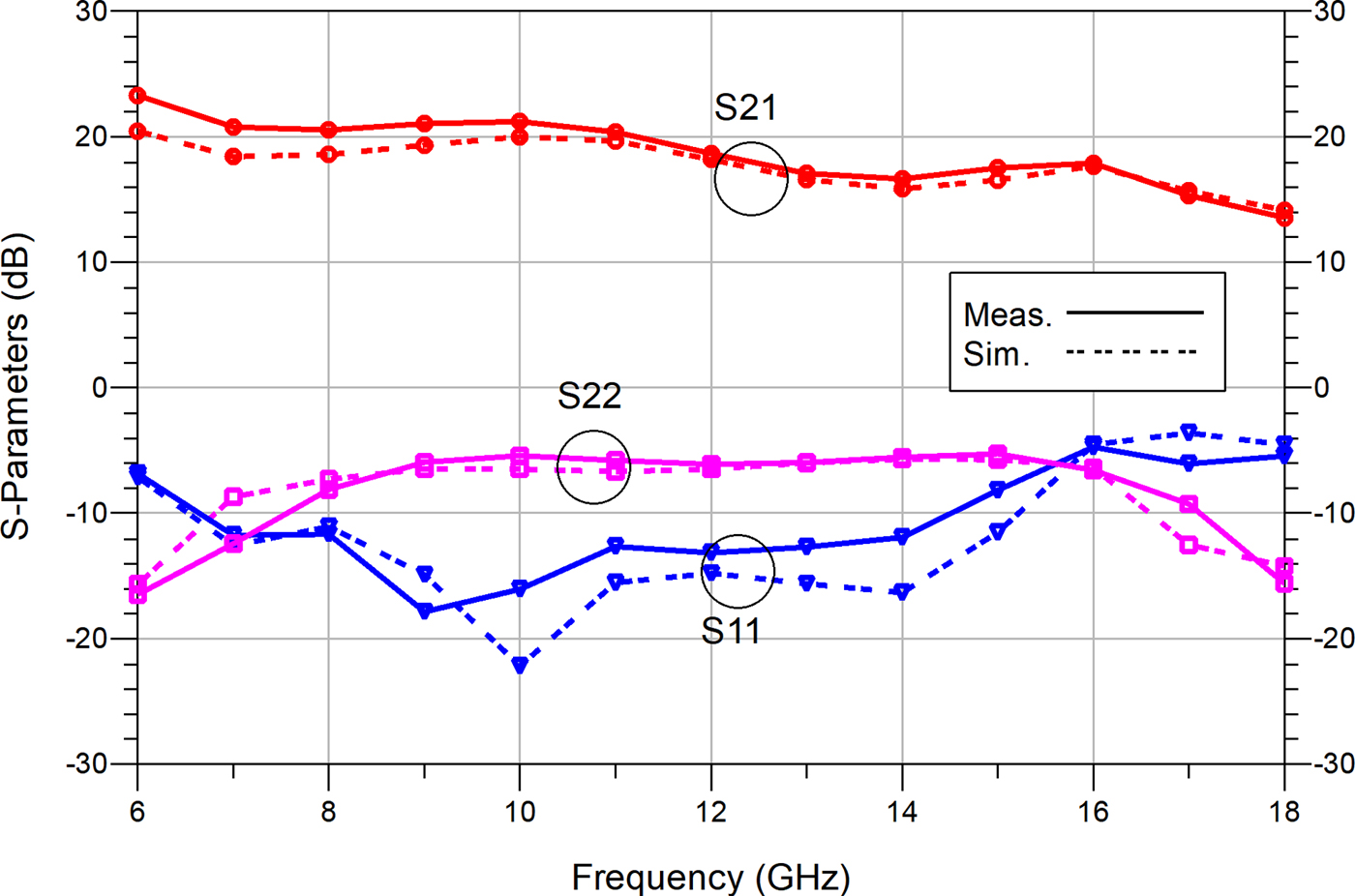
Both S-parameters and large signal measurements were performed and compared with simulations. These measurements were carried out using test probes in pulsed conditions for the large signal measurements and at ambient temperature without any heat sink. Fig. 10 shows the small signal response of the amplifier. Good agreement between simulations and measurements has been achieved, which suggests a good transistor model over the whole bandwidth. The amplifier exhibits a small signal gain of 23 dB at 6 GHz and 13 dB at 18 GHz. The result on S11 was good over the working bandwidth, except from 16 to 18 GHz, with a maximum value of −5 dB.
Small signal simulations and measurements on wafer.
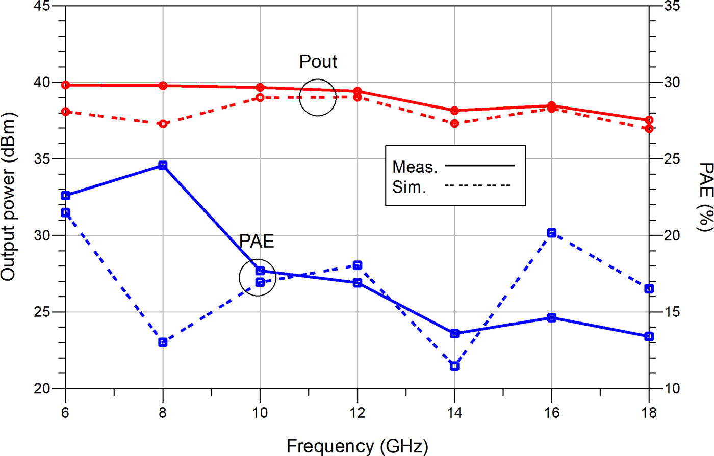
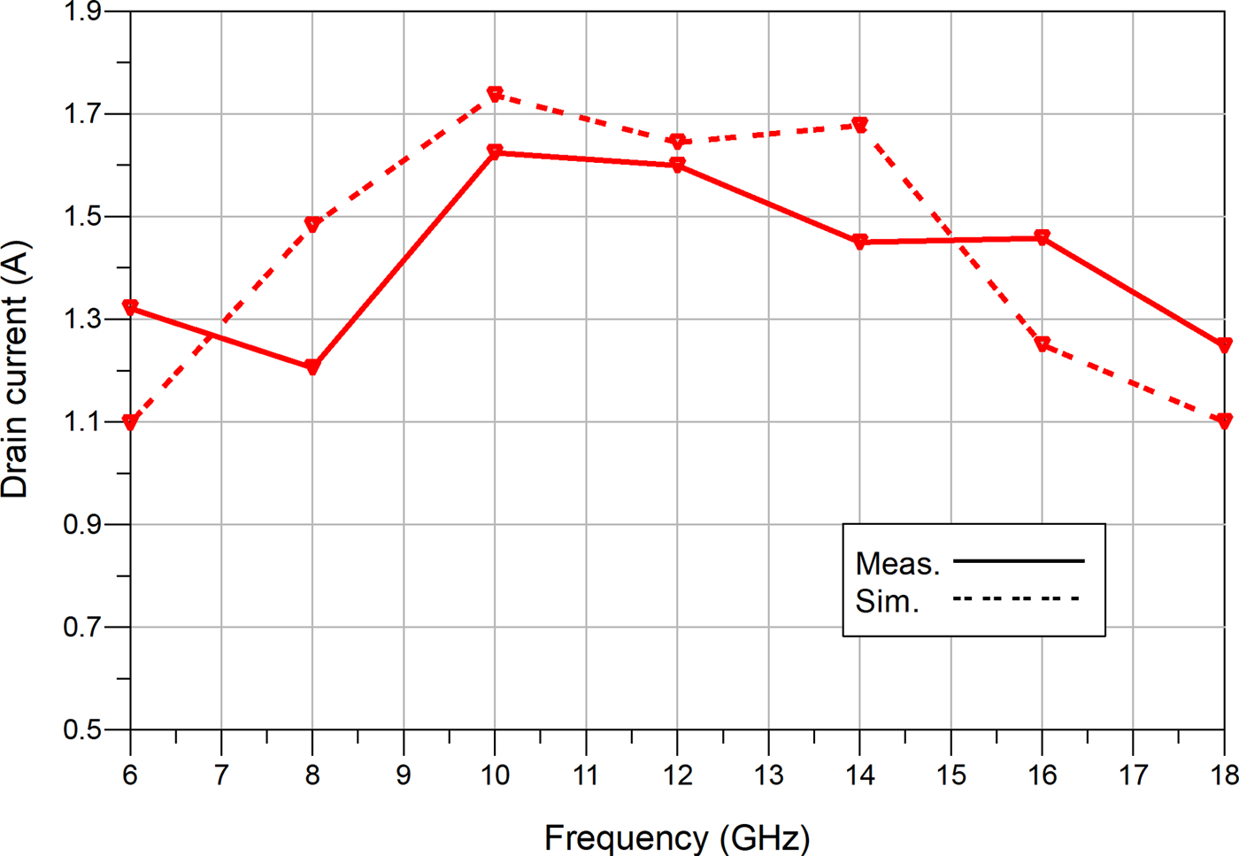
The output power and PAE for a fixed input power of 28 dBm are shown in Fig. 11. From 6 to 12 GHz, the measured output power was higher than 39 dBm, while from 12 to 18 GHz, the measured power was higher than 37 dBm. This can be explained because the last stage cannot reach the saturation point due to the power reflection caused by the S11 and the excess insertion loss in the inter-stage matching network at a high frequency as shown in Fig. 3. The current consumption was compared with the simulations as shown in Fig. 12. Some deviations were observed and they explain, in conjunction with the divergences in output power due to gain variations, the differences obtained in PAE results. Nonetheless, PAE is between 13.5 and 24.5% with a maximum current consumption of 1.6 A.
Large signal simulation and measurement on wafer for an input power of 28 dBm.
Drain current simulation and measurement on wafer.
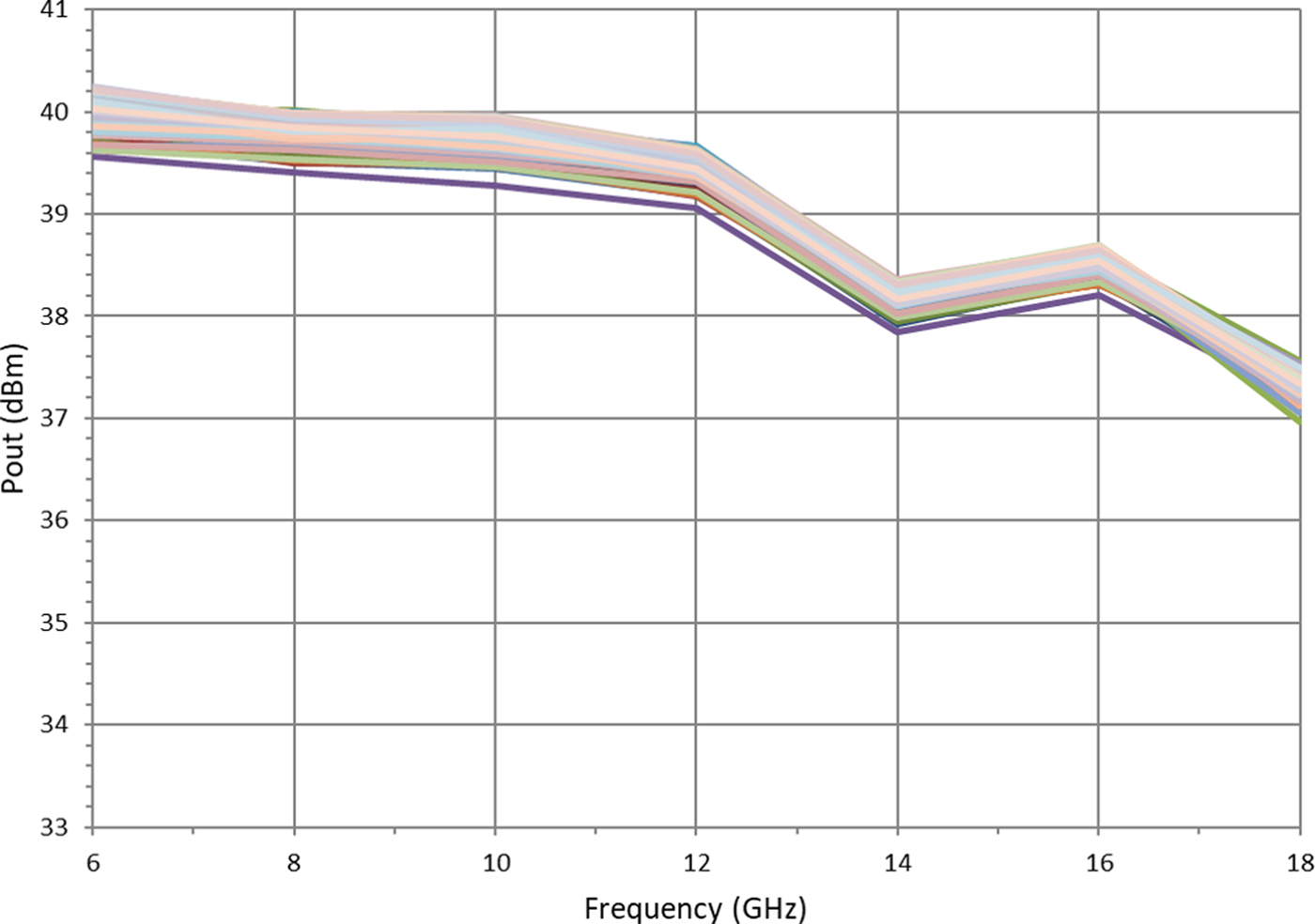
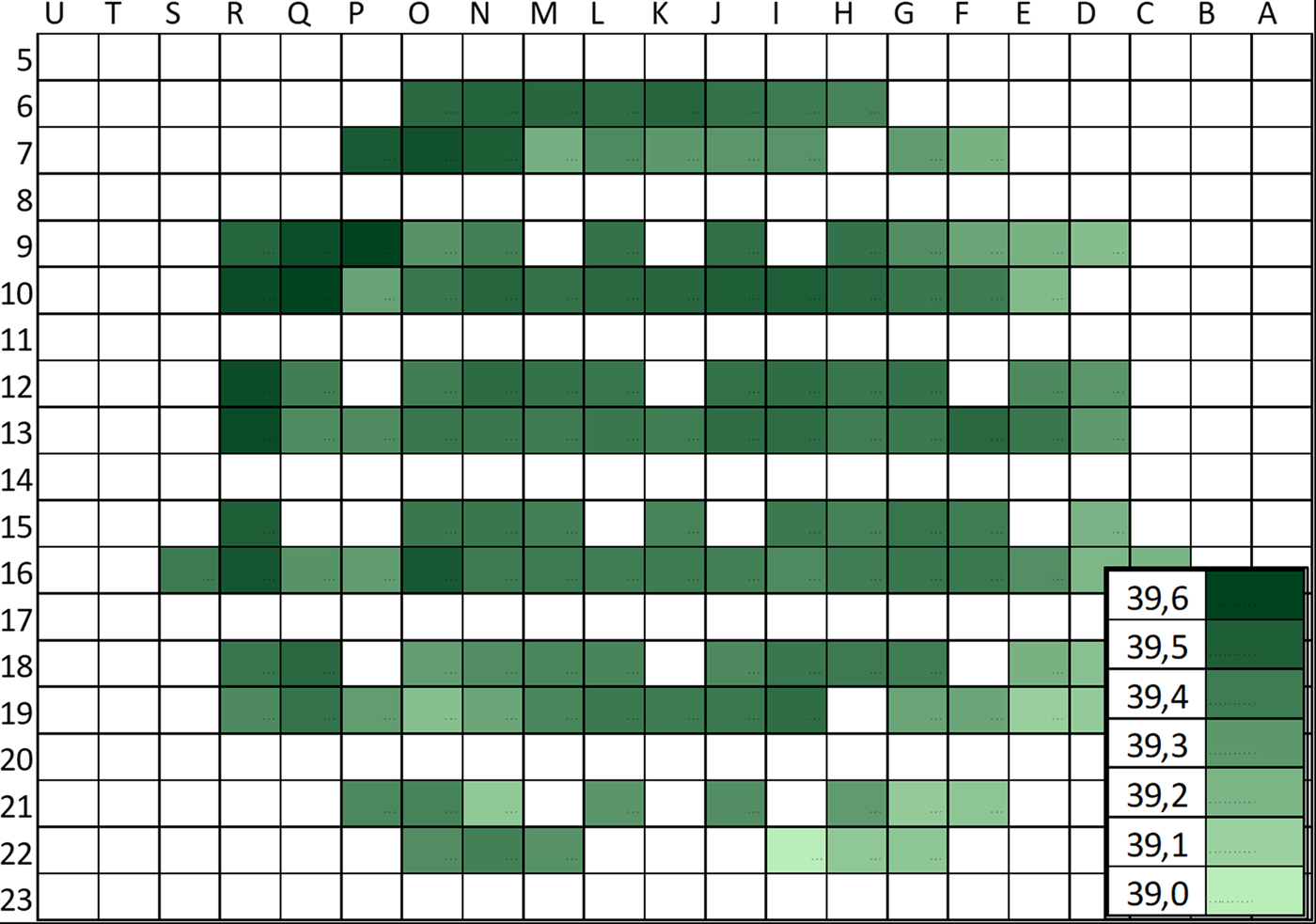
A statistical study using the data provided by the foundry was performed to characterize the complete wafer and foundry process in terms of repeatability and process variation. In Fig. 13, output power measured for all the amplifiers is depicted for an input power of 28 dBm. The maximum deviation among units is 0.68 dBm at 6 GHz. The mean output power for all the amplifiers was higher than 39 dBm. In Fig. 14, a schematic representation of the whole wafer is shown. The mean output power measured of each amplifier is represented using a color scale. It can be seen that, in this case, the amplifiers on the upper left corner achieve higher output power.
Output power spread measured for all power amplifiers on wafer for an input power of 28 dBm.
Distribution of mean output power measured per chip on wafer.
On jig measurements
Finally, the amplifier was mounted on the CuW jig as described in section ‘Assembly’. The jig was fixed to a test bench with a temperature-controlled baseplate. It comprised a 10 mil Duroid 5880 PCB, which includes the necessary RF and power supply lines and capacitors, single-layer decoupling capacitors for each supply voltage, and the HPA connected with gold bond wires as shown in Fig. 15. SMA end launch connectors were used to perform the measurements. The test bench is composed of the temperature-controlled plate, two DC power supplies with a current meter, one signal generator, a preamplifier, and a precision power meter. All the equipment used were calibrated to discount their effect on the measurement and were connected to a PC in order to control each equipment. The base plate temperature was configured at 25°C. This is because the amplifier will be integrated into a system that ensures this maximum base plate temperature by using a liquid cooling system.
HPA attached on the CuW jig.
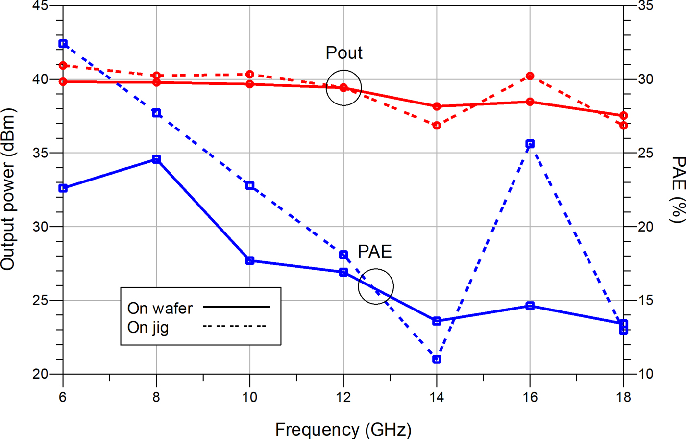
Pulsed and continuous wave measurements were carried out. The pulsed wave was configured as described at the beginning of this section. The results shown for the measurements on jig have no de-embedding of any element; therefore, the reference planes are at the end-launch connectors used to measure. In Fig. 16, a comparison between pulsed and continuous wave output power measurements is shown. It also shows the output power achieved for several input power levels. The maximum difference of output power between these two setups was 1.3 dB higher than the continuous wave for 28 dBm of input power at 18 GHz. This slight difference is due to the temperature-controlled plate, which evacuates properly the heat generated with high input power levels in a continuous wave configuration. Those results imply a mean gain at 28 dBm of input power of 11.3 dB for pulsed wave and 10.4 dB for continuous wave. In Fig. 17, the on wafer and on jig measurements for output power and PAE are depicted. The main differences come from the different measurement setup and the loss not de-embedded. The source and load impedances that the amplifier sees when it is mounted on the jig are different to 50 Ω because of the use of bond wires, the RF traces, and the end launch connectors. In addition, the use of a temperature-controlled base can affect the results.
Output power measured on jig over frequency depending on input power. Left: continuous wave. Right: pulsed wave.
Output power measured and PAE results on wafer and on jig comparison.
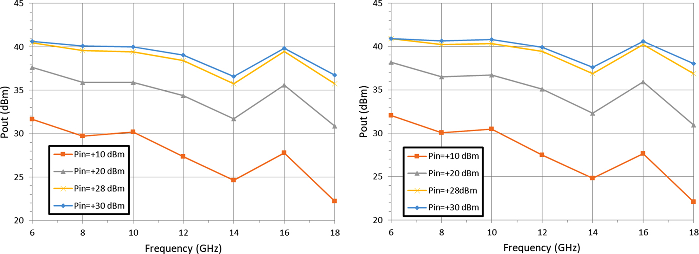
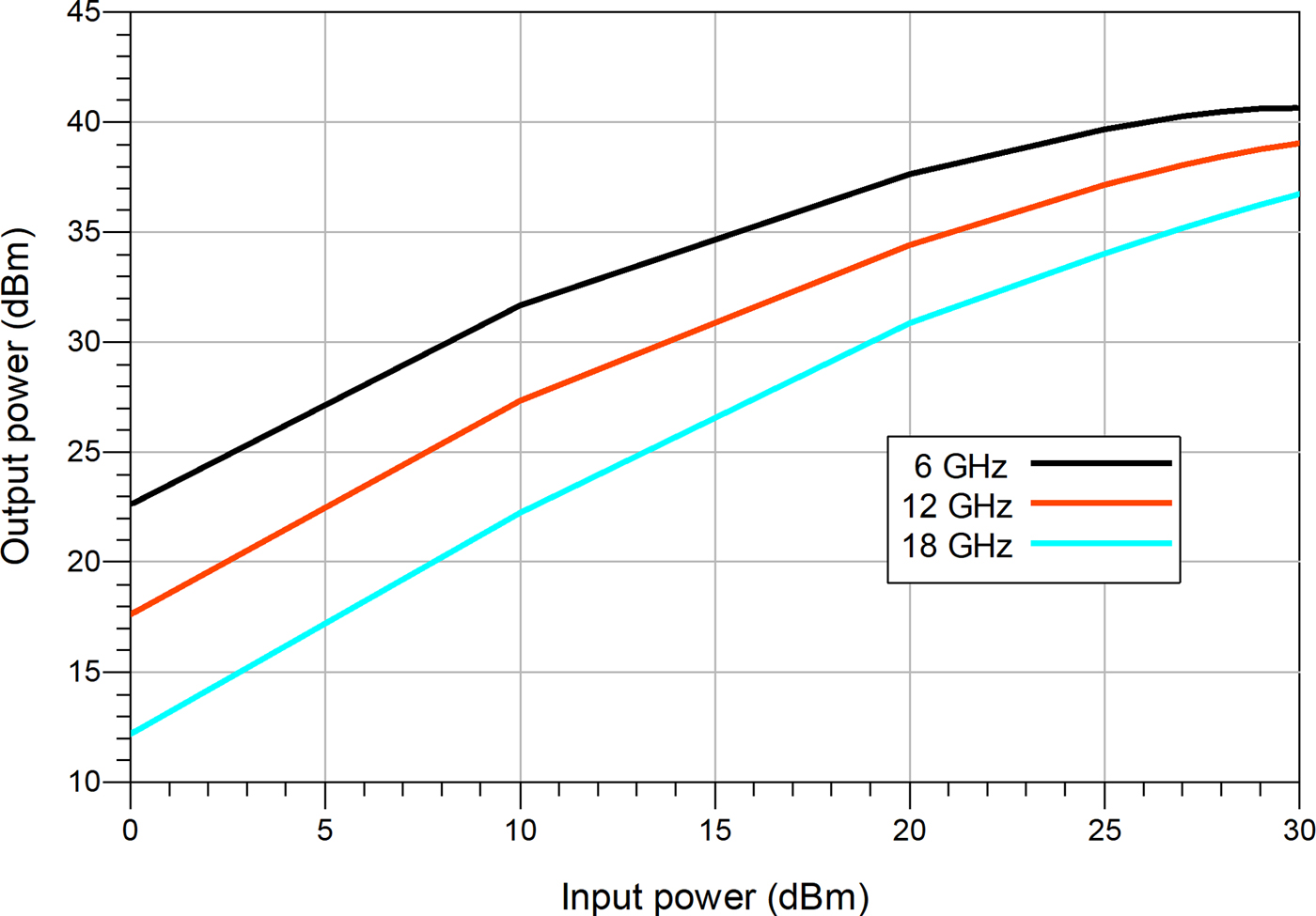
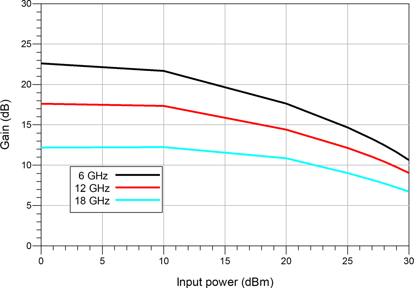
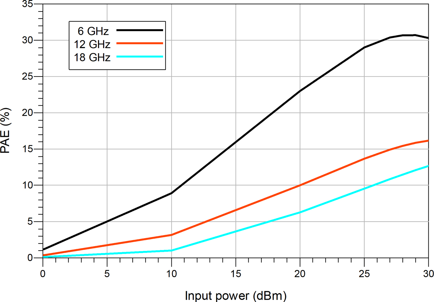
Output power and gain as a function of input power for 6, 12, and 18 GHz are depicted in Figs 18 and 19. In these figures, it can be seen that because the output transistors are not in saturation at high frequency, the output power achieved at high frequency is lower than the desired. PAE and drain current measurements as a function of input power are depicted in Figs 20 and 21. The results obtained in these measurements differ slightly from the on wafer measurements as said in the previous paragraph.
Output power measured on jig over an input power sweep for various frequencies.
Gain measured on jig over an input power sweep for various frequencies.
PAE measured on jig over an input power sweep for various frequencies.
Drain current measured on jig over an input power sweep for various frequencies.

Conclusions
A two-stage 6–18 GHz HPA on a 0.25 µm GaN on SiC process was designed and characterized. The design steps to select the transistor size, synthesize the impedance matching networks, and analyze the stability have been explained. The measurements on wafer and on jig show a saturated output power higher than 39 dBm up to 12 GHz and higher than 37.5 dBm up to 18 GHz. The mean gain in saturation over the whole bandwidth is 11 dB. PAE, which is in the range 13.5–24.5%, is affected by the differences in drain current and gain between simulations and measurements. Stability analyses for small and large signal have been done and the results ensure an unconditionally stable amplifier. Large signal stability analysis using the pole-zero technique was shown. Thermal analyses and different attachment method tests have allowed selecting the best way to simplify the MMIC assembly with epoxy of high thermal conductivity.
Acknowledgement
The authors wish to thank the partial support provided by the Ministerio de Industria, Energía y Turismo of the Spanish Government under project TSI-100103-201-32 APIGAN.
 Eduardo Oreja Gigorro received the B.S. degree in Telecommunication Engineering from the Universidad Carlos III de Madrid, Spain, in 2010. He joined Indra Sistemas in 2010 as an engineer in practices supporting the development of various units for Electronic Warfare systems. Since 2013 he is part of the microwave design group and has contributed and managed the design of passive and active microwave elements and devices, narrowband and broadband, assembled in maritime, terrestrial and aerial military vehicles. His main research interest is the design of broadband microwave devices and systems.
 Emilio Delgado Pascual received his M.Sc. degree in Telecommunication Engineering in 2014 and his M.Sc. degree in Data Science in 2018. He is developing his career as an RF/Microwave Engineer in Indra Sistemas since 2014, working in the fields of power amplifiers and high-frequency circuits. His current interests involve high-end microwave circuits, power amplifiers, autonomous CAD tools, and MMIC design.
 Juan José Sánchez Martínez received the B.S., M.S., and Ph.D. degrees in Telecommunication Engineering from the University of Málaga, Málaga, Spain, in 2003, 2006, and 2014, respectively. From 2006 to 2014, he was a Research Assistant with the Department of Communication Engineering, University of Málaga. He was involved with signal processing for digital communications and real-time implementation of signal processing algorithms on FPGA until 2010. From 2010 to 2014, he focused on the analysis of planar structures and the design of microwave passive devices. In 2014, he joined Indra Sistemas (Spain). The main tasks are focused on the analysis, design, and development of electronic measures (ESM) and electronic countermeasures (ECM) systems for air and naval applications. From May to August 2012, he was a Visiting Scholar with the Department of Electrical and Electronic Engineering, Imperial College London, London, UK. Dr. Sánchez-Martínez was the recipient of a Junta de Andalucía Scholarship (2010–2014).
 María Luz Gil Heras received a degree in Electronic Engineering from the University of Alcalá in 2000. PMP certified in 2014. She now works in Technology and Strategy in the Technology and Product Management Department in Indra Sistemas. She joined Indra in 2000 and is involved with them in the development of most important fulfilled EW projects in this company.
 Virginia Bueno Fernández received a degree in Telecommunication Engineer from the University of Alcalá. She has participated in radiofrequency design and development tasks in different projects at Indra. Currently, her main activities are coordination and management issues in the Microwave Area.
 Antonio Bódalo Márquez was born in 1963 at Madrid, developed Telecommunications Engineer studies, with Telecommunications Engineer Title obtained in 1989. Since then, he has worked at Indra Sistemas S.A. developing RF designs. Today he holds the role of RF&Mw Engineer Manager. His carrier is focused on design, development, and deployment of RF & Microwave designs such as Radar modules, IFF, Radar Warning, Wideband MCMs, and MMICs. For today and in the future, his compromise includes integration in MMIC designs as much as SoC for Wideband Receiver Components.
 Jesús Grajal was born in Toral de los Guzmanes (León), Spain, in 1967. He received his Ingeniero de Telecomunicación degree and the Ph.D. degree from the Universidad Politécnica de Madrid, Madrid, Spain, in 1992 and 1998, respectively. Since 2017 he has been a Full Professor at the Signals, Systems, and Radiocommunications, Department of the Universidad Politécnica de Madrid. His research activities are in the area of hardware design for radar systems, radar signal processing, and broadband digital receivers for radar and spectrum surveillance applications. Dr. Grajal was a co-recipient of the 2013 EuCAP best antenna design paper award.


