


Introduction
Tin monosulfide solar cells have attracted increasing attention as a potential low-cost and environmental friendly substitute for the commercial thin-film solar cells based on CdTe and CIGS [Reference Ramakrishna Reddy, Koteswara Reddy and Miles1, Reference Sinsermsuksakul, Hartman, Kim, Heo, Sun, Park, Chakraborty, Buonassisi and Gordon2, Reference Sinsermsuksakul, Sun, Lee, Park, Kim, Yang and Gordon3, Reference Jaramillo, Steinmann, Yang, Hartman, Chakraborty, Poindexter, Castillo, Gordon and Buonassisi4]. However, the thermodynamically stable phase of SnS (known as α-SnS) has two native properties that could limit its performance as a solar cell absorber. First, the orthorhombic double-layered crystal structure leads to highly anisotropic optical and electrical properties. The large effective mass reduces carrier mobility and, thus, impedes the collection of photoexcited carriers in the direction perpendicular to the planes of the layered SnS [Reference Albers, Haas, Vink and Wasscher5, Reference Abrikosov, Bankina, Poretskaya, Shelimova and Skudnova6, Reference Vidal, Lany, d’Avezac, Zunger, Zakutayev, Francis and Tate7]. Second, the α-SnS has an indirect band gap of 1.1 eV and a direct band gap exceeding 1.3 eV, which tends to reduce the achievable open-circuit voltage by up to 0.2 eV [Reference Vidal, Lany, d’Avezac, Zunger, Zakutayev, Francis and Tate7, Reference Tritsaris, Malone and Kaxiras8, Reference Sinsermsuksakul, Heo, Noh, Hock and Gordon9, Reference Miles, Ogah, Zoppi and Forbes10]. As a potential solution, the cubic phase of SnS has been investigated since the 1960s, although the phase assignment to rock salt or zinc blende has been debated [Reference Badachhape and Goswami11, Reference Mariano and Chopra12, Reference Avellaneda, Nair and Nair13, Reference Gao, Shen and Sun14, Reference Burton and Walsh15]. Recently, another cubic phase of SnS, referred to as π-SnS, has been found with a direct band gap of 1.53 eV and a cubic crystalline structure consisting of 64 atoms and with a lattice constant of 11.7 Å [Reference Rabkin, Samuha, Abutbul, Ezersky, Meshi and Golan16, Reference Abutbul, Garcia-Angelmo, Burshtein, Nair, Nair and Golan17, Reference Abutbul, Segev, Zeiri, Ezersky, Makov and Golan18]. The crystallographic structure and lattice parameters of the α-SnS, rs-SnS, and π-SnS are shown in Fig. S1, and their respective diffraction peak positions are shown in Table S1.
Rock-salt SnS has been mostly obtained by solution processing methods at low temperatures of less than 80 °C [Reference Garcia-Angelmo, Romano-Trujillo, Campos-Álvarez, Gomez-Daza, Nair and Nair19, Reference Chalapathi, Poornaprakash and Park20, Reference Breternitz, Gunder, Hempel, Binet, Ahmet and Schorr21]. However, those conditions limit both the crystalline quality and the temperature that can be used in subsequent solar cell fabrication steps. Alternatively, there are reports of π-SnS deposited by atomic layer deposition (ALD) at temperatures up to 200 °C, but the π phase only dominates in films less than 100 nm thick, which is not surprising given that π-SnS is thermodynamically less stable than α-SnS. However, the 50 nm-thick π-SnS films are too thin to be effective solar cell absorbers [Reference Baek, Pyeon, Song, Chung, Kim, Baek, Kim, Kang, Choi, Hwang, Han and Kim22, Reference Bilousov, Ren, Törndahl, Donzel-Gargand, Ericson, Platzer-Björkman, Edoff and Hägglund23].
Alloying is a powerful method to control material properties such as band gap, electrical properties, and crystal lattice constant [Reference Ning, Dou and Yang24, Reference Lou, Zhou, Kim, Alghamdi, Gong, Feng, Wang, Ye and Gordon25, Reference Bakke, Tanskanen, Hägglund, Pakkanen and Bent26]. Recently, a phase diagram was proposed for (Sn,Ca)S films, showing a transition from an orthorhombic phase to a cubic phase as calcium content increased [Reference Holder, Siol, Ndione, Peng, Deml, Matthews, Schelhas, Toney, Gordon, Tumas, Perkins, Ginley, Gorman, Tate, Zakutayev and Lany27, Reference Vidal, Lany, Francis, Kokenyesi and Tate28, Reference Matthews, Holder, Schelhas, Siol, May, Forkner, Vigil-Fowler, Toney, Perkins, Gorman, Zakutayev, Lany and Tate29]. Thus, the cubic phase can be obtained for films thick enough for solar cell absorbers. Vidal et al. showed that orthorhombic SnS can be converted into rock salt type by alloying with CaS [Reference Vidal, Lany, Francis, Kokenyesi and Tate28]. While orthorhombic SnS is energetically favorable, they demonstrated that the rock-salt phase (space group  $fm3\bar{m}$) has a formation enthalpy only 0.08 eV above that of the orthorhombic phase. This slight difference can be overcome by alloying SnS with CaS, at Ca fractions in excess of 0.18. In such case, (Sn,Ca)S thin films undergo a phase transition from orthorhombic (space group 62) to rock salt (space group 225). Because the mixing enthalpy is in the order of 100 meV, there should exist a miscibility gap under thermodynamic equilibrium conditions. This suggests the possibility of phase separation under certain conditions. However, the pulsed laser deposition and co-sputtering methods used to make the (Sn,Ca)S thin films in those papers require high vacuum and demand high processing temperatures, leading to high processing cost, significant loss of Sn, and difficulties in controlling the stoichiometry of the films. ALD allows precise control of film of stoichiometry, where one can easily engineer the film composition by controlling the dose ratio of different precursors [Reference Miikkulainen, Leskelä, Ritala and Puurunen30, Reference Johnson, Hultqvist and Bent31, Reference George32]. High-quality SnS and CaS thin films have been successfully deposited by ALD using various precursors [Reference Sinsermsuksakul, Heo, Noh, Hock and Gordon9, Reference Baek, Pyeon, Song, Chung, Kim, Baek, Kim, Kang, Choi, Hwang, Han and Kim22, Reference Bilousov, Ren, Törndahl, Donzel-Gargand, Ericson, Platzer-Björkman, Edoff and Hägglund23, Reference Rautanen, Leskela, Niinisto, Nykhen, Soininen and Utriainen33, Reference Hanninen, Mutikainen, Saanila, Ritala and Leskela34, Reference Kim, Yang, Powers, Davis, Lou and Gordon35, Reference Park, Heasley, Sun, Steinmann, Jaramillo, Hartman, Chakraborty, Sinsermsuksakul, Chua, Buonassisi and Gordon36, Reference Catherall, Harris, Hill, Johnson and Mahon37, Reference Yang38]. Our record SnS solar cell was deposited using in-house developed Sn(II) precursors at substrate temperatures lower than 200 °C [Reference Sinsermsuksakul, Sun, Lee, Park, Kim, Yang and Gordon3, Reference Yang38]. A newly developed Ca precursor has significantly lowered the CaS ALD temperature window to 150–275 °C, which allows an overlap of the CaS and SnS ALD windows and, thereby, enabling (Sn,Ca)S alloy formation using layer-by-layer deposition of SnS and CaS [Reference Kim, Yang, Powers, Davis, Lou and Gordon35].
In this study, we report ALD of rock-salt (Sn,Ca)S films with controllable composition at relatively low substrate temperatures. Crystal structure of the films is characterized before and after a high-temperature annealing process. Electrical and optical properties are also analyzed to demonstrate the possibility of using it as solar cell absorber materials.
Results and discussion
Film deposition using Sn and Ca precursors with different ligands
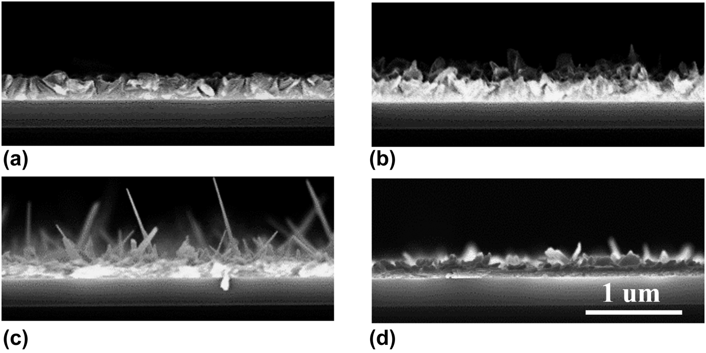
Alternating SnS and CaS cycles were deposited on thermal oxide substrates using Sn(A-amd)2 and Ca(F-amd)2, respectively, as the cation precursor and H2S as the sulfur precursor. Figure 1 shows the morphology of films deposited with a SnS:CaS cycle ratio of 20:1 at four different temperatures between 160 and 245 °C. Although we operated in the overlapping ALD temperature windows of SnS and CaS as shown in previous studies [Reference Sinsermsuksakul, Heo, Noh, Hock and Gordon9, Reference Kim, Yang, Powers, Davis, Lou and Gordon35], rough and spiky films were obtained over a wide range of temperatures and film smoothness decreased with increasing temperature. The flake and needle formation indicates high degree of anisotropic film growth, which could be a result of combining the orthorhombic SnS and rock-salt CaS growth, although this effect was not manifested in the individual binary film growth.
Cross-sectional SEM of (Sn,Ca)S deposited by Ca(F-amd)2 and Sn(A-amd)2 at different substrate temperatures: (a) 160 °C, (b) 190 °C, (c) 212 °C, and (d) 245 °C.

Figure 2 shows the composition and uniformity of the as-deposit ternary films estimated from X-ray photoelectron spectroscopy (XPS), as denoted by the atomic ratio of Ca/(Ca + Sn). The difference in Ca atomic ratio is high at the inlet of the reactor and increases from 0.21 to 0.67 as temperature increases, indicating more effective Ca incorporation at high growth temperatures. However, the calcium precursor shows a strong tendency to deplete near the furnace outlet as shown by the steep crease in Ca percentage among the cations as samples were placed further away from the precursor inlet at 245 °C. Oppositely, deposition at 160 °C saw a significant rise in Ca content toward the outlet.
Composition at different locations in the hot-wall tube ALD reactor of the (Sn,Ca)S film deposited at different temperatures. (a) Schematic diagram sample location across the 12 in substrate holder inside an approximately 18 in long hot-wall tube reactor - sample 1 is closest to the precursors inlet and sample 8 is closest to outlet to a roughing pump. (b) Atomic ratio of Ca/(Ca + Sn) estimated by XPS.

Figure 3 compares the calcium content measured by XPS with predictions from a simple additive model using the individual SnS and CaS ALD growth rate. Compositions of the inlet samples were used to avoid the complication of possible precursor depletion across the furnace. In the additive model, the growth rate of (Sn,Ca)S was assumed to be equal to the sum of the growth rates of binary SnS and CaS films when they are being deposited separately, which were measured to be 0.33 and 0.9 Å/cycle, respectively, within the present temperature window. Figure 3(a) shows that the alloy films deposited at all temperatures had higher Ca content than the additive model prediction, where the atomic ratio of Ca/(Ca + Sn) was calculated to be 0.12. Furthermore, the SnS:CaS cycle ratio was varied from 35:1 to 5:1 at a fixed temperature of 212 °C to study the effect on composition. Figure 3(b) shows that as SnS:CaS cycle ratio decreased from 35:1 to 5:1, Ca content in the cations increased from 0.33 to 0.95, which was again much higher than the additive model predictions of 0.07–0.35.
Composition of (Sn,Ca)S deposited by Ca(F-amd)2 and Sn(A-amd)2 (a) at different temperatures using SnS:CaS dosing ratio of 20:1 and (b) using SnS:CaS dosing ratio ranging from 5:1 to 35:1 at substrate temperature of 212 °C. The blue square represents experimentally observed value, and the black dot represents the calculated value under the ideal mixture assumption.

Both the spiky film morphology and the discrepancy between predicted and actual composition are difficult to explain by the conventional ALD model, where the layer-by layer-growth and self-saturated surface reaction should result in smooth and stoichiometric films. To examine the cause, we investigated the growth mechanism of the (Sn,Ca)S ternary film using a quartz crystal microbalance (QCM), which measured the in situ mass changes of the growing film. The quartz crystal was placed near the inlet of the precursors. Figure 4(a) shows the mass changes of fifteen SnS cycles followed by one CaS cycle at a temperature of 212 °C. Figure 4(b) compares the mass change of one CaS cycle inserted into a (Sn,Ca)S deposition and that in bulk CaS deposition. After Ca(F-amd)2 dose and purge of excess precursor, mass gain in the ternary film was 40% less than that in bulk CaS. One may attribute this to less effective adsorption of Ca(F-amd)2 onto a surface finished with –Sn–S–H groups from previous SnS growth cycles. However, we were more surprised to see that after H2S dose and purge, there was also approximately twice the amount of mass loss, leading to a net mass loss during the CaS deposition cycle. Given that XPS data showed 5× higher Ca content than prediction under this deposition condition, we suspect that significant amount of cation replacement of Sn by Ca might have happened during the Ca(F-amd)2 dose. Similar ion exchange processes have been observed in the atomic layer deposition of other metal sulfide systems [Reference Thimsen, Peng, Martinson, Pellin and Elam39]. The cation exchange reaction between Ca(F-amd)2 precursors and underlaying SnS can be described as:
 $${\rm{SnS}}\left( {\rm{s}} \right) + {\rm{Ca}}{\left( {{\rm{F ‐ amd}}} \right)_{\rm{2}}}\left( {\rm{g}} \right) \to {\rm{CaS}}\left( {\rm{s}} \right) + {\rm{Sn}}{\left( {{\rm{F ‐ amd}}} \right)_{\rm{2}}}\left( {\rm{g}} \right)\quad .$$
(a) Mass changes as measured by QCM during (Sn,Ca)S deposition using SnS:CaS dose ratio of 15:1. (b) Comparison of mass change in one CaS ALD cycle in a bulk CaS film (blue) and in the alloy deposition (red).

During this cation exchange reaction, Ca (atomic mass 40) replaces Sn (atomic mass 119), leading to a mass loss of −79 g/mol; whereas during the Ca precursor adsorption step, there would be a mass gain of 166 g/mol, which could balance the mass decrease due to the cation replacement of Sn by Ca. This is consistent with the QCM data, where the Ca dose/purge step led to a net mass gain that is lower than what the mass gain would be without the cation exchange. Similar replacement could also occur during the Sn(A-amd)2 pulse following the CaS ALD cycle. As shown in Fig. S2, QCM measurement of multiple super cycles of SnS and CaS deposition shows that the first SnS cycle following the CaS cycle has moderately higher growth rate than the subsequent SnS cycles, which indicates that cation exchange of the lighter Ca by the heavier Sn likely has occurred, although to lesser degree, and the film is, thus, still Ca rich. Further quantification would require more sophisticated experiment setup, possibly with in situ surface composition or gas phase species characterization capabilities.
To attain the actual Ca/(Ca + Sn) value of 0.62 with 1 CaS cycle among every 15 SnS cycles, it is estimated that approximately 9 out of 15 cycles of previously deposited SnS would need to be replaced by CaS. Given the SnS growth rate of 0.33 Å/cycle, it takes at least 12 cycles to grow one monolayer of SnS. Thus, despite the apparently high content of Ca, the cation replacement needs to only happen for less than 3/4 of topmost monolayer of SnS during the Ca(F-amd)2 dose to reach a Ca/(Ca + Sn) value of 0.62, which is not unreasonable. This cation replacement hypothesis could also qualitatively explain the increasing Ca content with temperature as the replacement is likely to be driven thermally and higher temperature could facilitate faster and more complete reaction. Ca(F-amd)2 would be consumed much faster when the Ca cations replace the Sn cations than growing only one layer of CaS alone as in bulk CaS growth, which is consistent with the faster depletion of Ca precursor across the furnace at high temperature. Furthermore, if a significant portion of the Sn in the previously deposited SnS was replaced by Ca, the crystal lattice would be disturbed and roughing of the film would not be unexpected. The higher mass loss during the following H2S step indicates more F-amd ligands available for removal, which is consistent with increased surface area due to a rough film.
Another hypothesis of the low Sn composition in (Sn,Ca)S ternary film is that after CaS ALD cycle, the resulting surface may not be favorable for the chemisorption of Sn precursors, especially at high substrate temperatures. However, the delay itself is insufficient to explain the 5× higher Ca content, and more QCM data in fact showed no noticeable delay in SnS growth immediately after the CaS cycle. Yet, one should still note that the QCM experiment has its own limitations in simulating actual film growth inside an ALD reactor. The growth substrate in QCM experiment is coated with gold, resulting to a different crystallographic orientation as compared with bulk SnS deposition on Mo or SiO2 substrates that were used for all our other depositions. Meanwhile, the substrate holder used to support quartz crystal has different geometry than that for bulk film deposition, which could lead to different gas transport kinetics that affect the QCM results.
Film deposition using Sn and Ca precursors with the same ligands
The rough and spiky morphology renders the films formed by Ca(F-amd)2 and Sn(A-amd)2 unsuitable for solar cell applications. As a new Sn precursor was being developed using the same F-amd ligand as the Ca precursor, we deposited the (Sn,Ca)S film again with Sn(F-amd)2 and Ca(F-amd)2 as the cation precursors, in an attempt to improve the film quality. Alternate cycles of SnS and CaS were deposited using Ca(F-amd)2 and Sn(F-amd)2, respectively, at different temperatures within the overlapping ALD temperature window from 135 to 190 °C and at different SnS:CaS cycle ratios. Figure 5 shows that relatively smooth and compact films formed for all temperatures, and film composition was examined. Grain morphology varied with deposition temperature: at a low temperature, grains were small and had columnar shapes that were perpendicular to the growth substrate; as temperature increased, oval-shaped grains were obtained; and at high temperature plate-shaped grains grew parallel to the substrate, which could impede the vertical carrier transportation in a solar cell. An SEM image of a 500-nm thick alloy film deposited at 190 °C shows the layered film with plate-shaped grains more clearly [Fig. 5(d)]. Figure 6 shows that the Ca contents are again higher than the values calculated from the separate growth rates of SnS and CaS using Ca(F-amd)2 and Sn(F-amd)2, indicating the presence of cation replacement as discussed in section “Film deposition using Sn and Ca precursors with different ligands”.
(a)–(c) Cross-section (top) and top-view (bottom) SEM of 100–200 nm of (Sn,Ca)S ternary films deposited by Sn(F-amd)2 and Ca(F-amd)2 at different temperatures using an SnS:CaS ALD cycle ratio of 15:1. The growth rates are estimated to be 6.3, 5.7, and 4.7A per super cycle. Cycle numbers are chosen so that the film thickness is 100–200 nm. (d) Cross-section SEM of an attempted solar cell with a 500-nm (Sn,Ca)S film deposited at 190 °C. In this structure, (Sn,Ca)S film was sandwiched between Mo growth substrate and sputtered ITO. (e)–(h) Cross-section (top) and top-view (bottom) SEM of 100–200 nm of (Sn,Ca)S films deposited at 160 °C using different ALD cycle ratios of SnS:CaS. Growth rates are in the rage of 4.6 to 6.8 A per super cycle.

Composition of (Sn,Ca)S deposited by Ca(F-amd)2 and Sn(F-amd)2 (a) at different temperatures using SnS:CaS dosing ratio of 20:1 and (b) using SnS:CaS dosing ratio ranging from 10:1 to 30:1 at substrate temperature of 212 °C. The blue square represents experimentally observed value, and the black dot represents the calculated value under the ideal mixture assumption.

Compared to films deposited by Ca(F-amd)2 and Sn(A-amd)2, films deposited by Ca(F-amd)2 and Sn(F-amd)2 showed smoother and more compact film morphology at the same deposition temperature of 160 and 190 °C. Thus, we postulate that ternary film deposition in ALD benefits from selecting precursors of the same ligands. This observation is difficult to explain in the conventional ALD context nor by our proposed cation replacement hypothesis. One possible hypothesis of such a morphology difference is that the roughness could result from an uneven competition for the surface –SH groups between F-amd and A-amd ligands. Further work needs to be carried out to fully understand the impact of precursor choice on film properties.
Structural properties
High-resolution X-ray diffraction (XRD) was performed on the alloy films, and the peak positions were compared with simulated diffraction peak positions of α-SnS, rs-SnS, π-SnS, and CaS to determine the crystal structure of the alloy films. As-deposited films were then annealed at 400 °C in 99.5% H2S at 10 torr for 1 h in the same furnace to study their stability. Figure 7(a) shows the in-house high-resolution X-ray diffraction (HRXRD) spectra of approximately 120 nm of (Sn,Ca)S films deposited at 160 °C with five different compositions. The pure SnS film demonstrates two sets of characteristic doublet peaks at around 27° and 31°, respectively. As calcium content increases in the as-deposited films, each set of doublet peaks starts to merge into a broader and weaker peak, respectively. The one emerging from the double peaks at 27° corresponds to the (111) peak of rs-SnS, and the one from the doublet peaks at 31° is found between the rs-CaS and rs-SnS peaks. We noted that the orthorhombic SnS film starts to convert to the cubic phase at approximately 17% Ca in the cation mix and reaches full conversion at approximately 33% Ca. However, the cubic phase is partially converted back into orthorhombic after annealing, and the α-SnS doublet peaks are recovered. This could be caused by phase separation into SnS and CaS at high temperature, which agrees with the thermodynamic argument by Vidal et al. [Reference Vidal, Lany, Francis, Kokenyesi and Tate28].
XRD spectra of (a) as-deposit and (b) annealed thin films (∼100 nm) with different Ca contents. The y-axis represents the percentage of Ca in the cation mix of Sn + Ca, and the bottom spectrum represents pure SnS. (c) Synchrotron-based 2DXRD integrated spectra of thicker film (∼600 nm) with Ca/(Ca + Sn) = 0.33. The peaks corresponding to different crystal structures are labeled by different markers. The light-colored dashed lines mean to serve as a guide to the eye.

A thicker film (600 nm) with composition near the phase transition (33% Ca) was deposited at 135 °C and examined by the synchrotron-based 2DXRD, which has higher resolution and beam intensity and can, thus, reveal more details in its crystal structure. These data were converted to 2-theta angles using Cu Kα radiation (λ = 1.542 Å) for easier comparison. Figure 7(b) shows the 2DXRD spectrum of an as-deposited and annealed film. All peaks in the as-deposited film are from π-SnS, with the strongest peaks being (400), (222), (440), and (622). This is consistent with the powder XRD patterns of π-SnS nanoparticles as presented by Abutbul et al. [Reference Abutbul, Garcia-Angelmo, Burshtein, Nair, Nair and Golan17, Reference Abutbul, Segev, Zeiri, Ezersky, Makov and Golan18]. However, it is worth noting that the (200) and (111) rock-salt peaks coincide with the (222) and (400) π-phase peaks, so we cannot exclude the possibility that the rock-salt phase also exists. Zooming into a smaller region, we can see that the three peaks between 31° and 33° have slight positive shifts compared to the reference peaks for pure SnS. These shifts indicate a slight lattice contraction caused by smaller calcium atoms occupying some of the tin sites. The direction of these shifts is surprising because standard tables of ionic radii suggest that calcium ions are larger than divalent tin ions. After annealing, all major peaks can be aligned with α-SnS, and the characteristic doublet peaks at 27° clearly reemerge. The assignment of peaks around 31° is less definitive because several peaks from different phases crowd into that region. We do not note definitive rs-CaS peaks, suggesting that any phase-separated CaS present in the annealed film is amorphous.
Electrical properties
Resistivities of films deposited at 135 and 160 °C were measured using the van der Pauw method. We can see in Fig. 8(a) that the resistivity increases with increasing amount of Ca in the film. One probable explanation is that as Ca atoms are incorporated into the SnS film, they occupy the Sn vacancies (V Sn), which is the major source of p-type conductivity [Reference Albers, Haas, Vink and Wasscher5, Reference Abrikosov, Bankina, Poretskaya, Shelimova and Skudnova6, Reference Vidal, Lany, d’Avezac, Zunger, Zakutayev, Francis and Tate7]. Films deposited at 160 °C have resistivities in the range of 102–104 Ω cm, but films deposited at 135 °C demonstrate much higher resistivities, possibly because of their smaller grain size and columnar-shaped grains which are aligned perpendicular to growth substrates. After annealing, the resistivities of all films decrease significantly, which may be caused by phase separation and grain growth. Figure 8(b) shows Hall measurement results both pre and postannealing. As expected, this sample has both very low carrier density (6.3 × 1014 cm−3) and low hole mobility (0.18 cm2/V s). Although both carrier concentration and hole mobility were increased upon annealing, they are still not ideal for solar cell absorbers. On the other hand, annealed films deposited at 160 °C have resistivity of 100–300 Ω cm, which could be suitable as absorbers.
(a) Resistivity of (Sn,Ca)S samples with different Ca content deposited at 160 and 135 °C, as-deposit (solid) and after annealing (unfilled). (b) Van der Pauw and Hall measurements of 600 nm of Sn0.67Ca0.33S deposited at 135 °C and after annealing at 400 °C in H2S environment for 1 and 2 h.

Optical properties
The absorption coefficient (α) and the optical band gap (E g) of the alloy film were determined from the transmittance (T) and reflectance (R) measurements using a Hitachi UV–Vis–NIR spectrophotometer. All of these films used for optimal measurement had a thickness between 120 and 160 nm as measured in SEM. E g is determined using the equation (αhν)n = A(hν − E g ± E ph), where A is a constant, n is the transition probability (n = 2 for direct-allowed transition and n = 1/2 for indirect-allowed transition), and E ph is the phonon energy [Reference Ritter and Weiser40]. Figure S3 shows the plots of (αhν)n versus photon energy for the (Sn,Ca)S films of different compositions. In the direct transition model, SnS has a direct band gap of 1.35 eV, which is close to previous experimental results [Reference Sinsermsuksakul41], and the band gap of alloy films is around 1.38 eV, with only a weak dependence of band gap on Ca content. It is worthwhile to note that there is stronger absorption in the subbandgap region in films with higher Ca, indicating more defect states close to the band edge. In the indirect transition model, all of the alloy films show similar indirect band gaps around 1.20–1.23 eV, which are 0.15 eV lower than direct band gaps.
Conclusions
In summary, (Sn,Ca)S alloy films with controllable composition were deposited by ALD using alternating cycles of H2S alternating with Ca(F-amd)2, Sn(A-amd)2, or Sn(F-amd)2. Using Sn and Ca precursors based on the same ligand enables deposition of dense and conformal films. Detailed time dependence of the deposition process shows that the previously deposited SnS is partially removed by calcium precursor vapor, which partially explains why the Ca contents in the alloy films are higher than those predicted from the separately measured growth rates of pure SnS and pure CaS. We found that (Sn,Ca)S transforms from an orthorhombic phase to a cubic phase as the Ca content increases. The presence of the cubic π-phase is verified using the synchrotron-based 2DXRD. XRD spectra of annealed films indicate that the cubic (Sn,Ca)S alloy films are converted to orthorhombic, likely due to phase separation into the thermodynamically stable phase of SnS. Resistivities of the as-deposited films are decreased by 1–2 orders of magnitude by annealing, further verifying our hypothesis that (Sn,Ca)S is a metastable material that undergoes phase separation during heating.
Experimental
The (Sn,Ca)S alloy films were deposited in a custom-built hot-wall ALD reactor by alternating SnS and CaS cycles using the recipe [(SnS)m–(CaS)]n, where m and n were integers used to adjust the composition and thickness of the film, respectively. Bis(N,N′-diisopropylformamidinato)calcium(II), referred to as Ca(F-amd)2, was used as the calcium source. Two kinds of tin sources were used: bis(N,N′-diisopropylacetamidinato)tin(II) and bis(N,N′-diisopropylformamidinato)tin(II), referred to as Sn(A-amd)2 and Sn(F-amd)2, respectively. These precursor compounds were heated to temperatures sufficient to provide enough vapor for growing films: Sn(A-amd)2 was maintained at 95 °C, Sn(F-amd)2 at 65 °C, and Ca(F-amd)2 at 135–140 °C. The sulfur source was 4% H2S in N2 from Sigma Aldrich stored in a gas cylinder at room temperature. The exposure time for all the amidinate precursors are set to be 1 s, and H2S was exposed 3 s in the reactor. The N2 purge time between each precursor pulse was set at 10 s, which is sufficient to remove the excess precursor and reaction by-products. The individual ALD processes for SnS [Reference Sinsermsuksakul, Sun, Lee, Park, Kim, Yang and Gordon3, Reference Sinsermsuksakul, Heo, Noh, Hock and Gordon9] and CaS [Reference Kim, Yang, Powers, Davis, Lou and Gordon35, Reference Yang38] have been published elsewhere. As-deposited thin films are annealed at 400 C for 1 h in H2S/N2 environment at a pressure of 4 torr.
Field emission scanning electron microscopy (FESEM; Zeiss Supra55VP) was used to examine film morphology and estimate thickness. Composition was obtained by X-ray photoelectron spectroscopy (XPS; Thermo Scientific K-Alpha). Crystal structure of the films is performed using both high-resolution X-ray diffraction (HRXRD; Bruker D8) (Cu Kα radiation, λ = 1.542 Å) θ–2θ scans and synchrotron-based 2DXRD (λ = 0.9744 Å) at beamline 11–3. The latter one is performed at the Stanford Synchrotron Radiation Lightsource (SSRL). Absorption spectra of the films were measured using a Hitachi U-4100 UV–Vis–NIR spectrophotometer.
Supplementary material
To view supplementary material for this article, please visit https://doi.org/10.1557/jmr.2019.337.
Acknowledgments
This research was supported in part by the Center for the Next Generation of Materials by Design, an Energy Frontier Research Center funded by the U.S. DOE, Office of Science. Part of the work was performed at the Center for Nanoscale Systems (CNS) at Harvard University, a member of the National Nanotechnology Infrastructure Network (NNIN), which is supported by the National Science Foundation under NSF award no. ECS-0335765. Use of the SSRL, SLAC National Accelerator Laboratory, was supported by the U.S. Department of Energy, Office of Basic Energy Sciences under Contract No. DE-AC02-76SF00515.


