





Introduction
Modern wireless communication standards rely on spectrally efficient linear modulation techniques sensitive to amplitude and phase errors. Such standards require high linear power amplifiers (PA) in the RF front-end modules to avoid interference with the adjacent channels [Reference Asbeck, Rostomyan, Ozen, Rabet and Jayamon1]. The well-known trade-off between efficiency and linearity, where the linearity declines at peak power efficiency, results in PA operation at backoff power levels below the maximum saturated output power (PSAT) to meet the linearity specifications. Amplitude-to-amplitude (AM/AM) distortion and amplitude-dependent phase distortion (AM/PM) are known contributors to spectral regrowth, with the latter additionally causing difficulties in the received signal detection. Their combined contribution results in out-of-band interference of the transmitted signal and bit errors of the received signal [Reference Sen, Devarakond and Chatterjee2].
Downscaled GaN HEMTs are capable of meeting the challenging output power and efficiency requirements set by modern RF and high-power applications [Reference Fletcher and Nirmal3]. Nevertheless, these devices are renowned for their non-linear behavior chiefly stemming from the transconductance derivatives and bias-dependent capacitances [Reference Sarbishaei, Wu and Boumaiza4]. Furthermore, short-channel GaN HEMTs employ T-shape gates for a larger cross-sectional area to reduce the gate-line resistance, thereby improving the cut-off frequency of the unilateral gain (fMAX). The field plates, which are connected to the gate electrically and kept at a distance above the semiconductor surface, offer a conducting plane which reduces the high electric field peaks that result in an electronic breakdown [Reference Trew, Bilbro, Kuang, Liu and Yin5]. This electric field reduction at the gate edge allows the application of high voltages and subsequently higher output powers. However, their presence involves trade-offs between device parasitics, including the gate-to-drain capacitance, which influences fMAX and the device linearity.
Extending our work presented in [Reference ElKashlan, Khaled, Rodriguez, Putcha, Peralagu, Alian, Collaert, Wambacq and Parvais6], we aim to provide in this paper an understanding of the trade-offs associated with T-gate geometry optimization through additional small-signal modeling and large-signal characterization. The results of the non-linear characterization of several geometrical configurations show the necessity of optimizing the gate-to-drain field plate (lgfp) for an appropriate trade-off of the phase and harmonic distortion, where phase distortion is mitigated with lgfp downscaling at the expense of the harmonic distortion and gain linearity.
The GaN HEMT devices
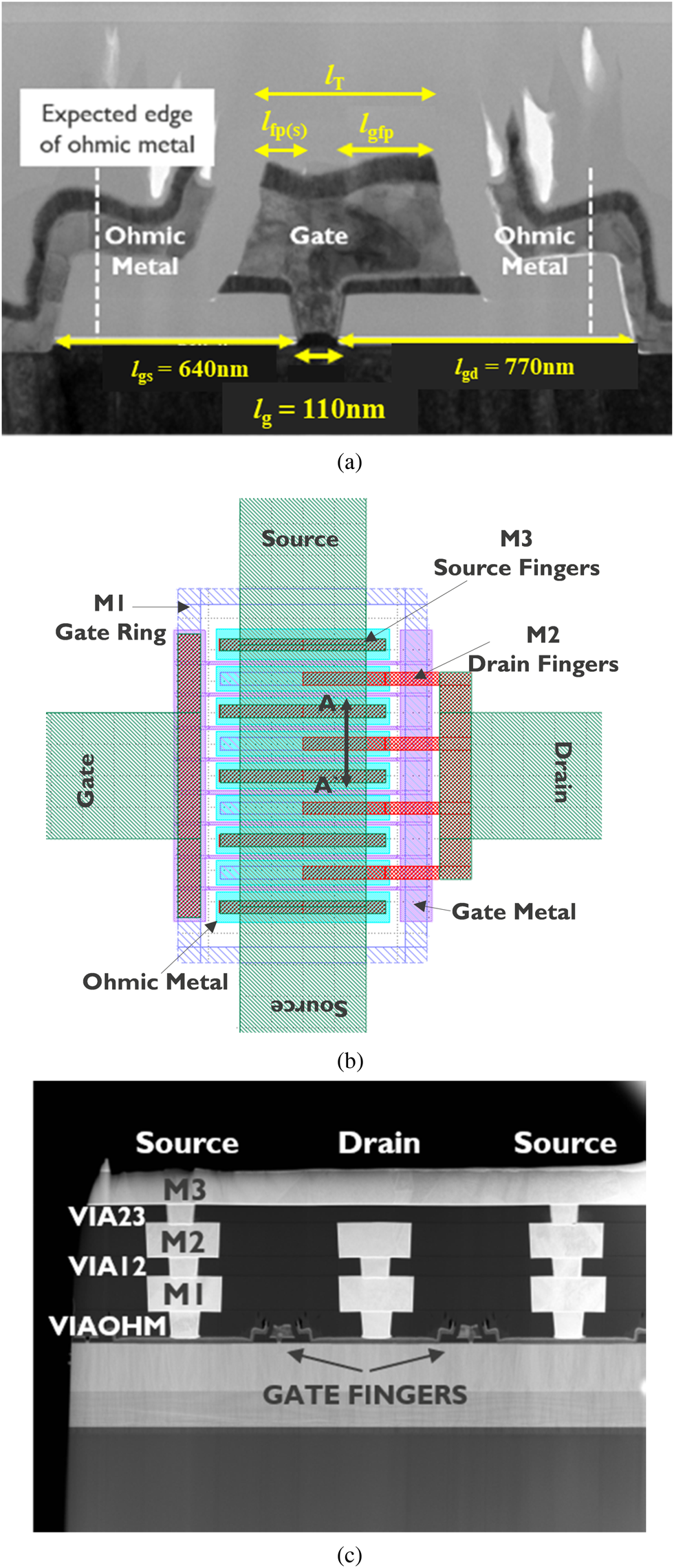
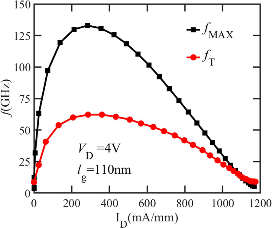
The devices under test (DUTs) are eight-finger AlGaN/GaN HEMTs fabricated in a three-level Cu damascene back end of line (BEOL) process on 200 mm Si wafers (Fig. 1) [Reference Parvais, Alian, Peralagu, Rodriguez, Yadav, Khaled, ElKashlan, Putcha, Sibaja-Hernandez, Zhao, Wambacq, Collaert and Waldron7, Reference Peralagu, Alian, Putcha, Khaled, Rodriguez, Sibaja-Hernandez, Chang, Simoen, Zhao, De Jaeger, Fleetwood, Wambacq, Zhao, Parvais, Waldron and Collaert8]. The ohmic contact resistance (RC) is ~0.15 Ω.mm, and the sheet resistance (RSH) is ~370 Ω/sq. There is an increase in the parasitic capacitance of these DUTs because the ohmic metal moved closer to the gate head than anticipated, on both the source and drain sides, during the device processing. For an 110 nm device, the maximum ID is ~1.2 A/mm, and the peak fMAX is 135 GHz, whereas this processing issue limits the peak fT to 60 GHz (Fig. 2).
(a) TEM cross-section of a 110 nm device with the definition of the dimensions. (b) Eight-finger GaN HEMT device layout with three BEOL metal layers. (c) TEM cross-section across the A-A″ cutline shown in (b) highlighting the three Cu layers.
fT/fMAX versus bias for the shortest device at VD = 4 V. Device geometry: lg = 110 nm, lgfp = 250 nm, lfp (s) = 120 nm, lgs = 540 nm, lgd = 670 nm, NF × WF = 8 × 25 μm.
To study the impact of varying the T-gate geometries, we consider lgfp ranging from 50 to 450 nm and gate-to-source field plates (lfp (s)) of 50 and 120 nm. The downscaled gate-drain (lgd) and gate-source (lgs) spacings are adjusted according to the lgfp, lfp (s) lengths to maintain a constant effective gate-to-drain and gate-to-source distances. The devices have an off-state lateral breakdown voltage (VBD) of ~105 V at a breakdown criterion of 1 mA/mm.
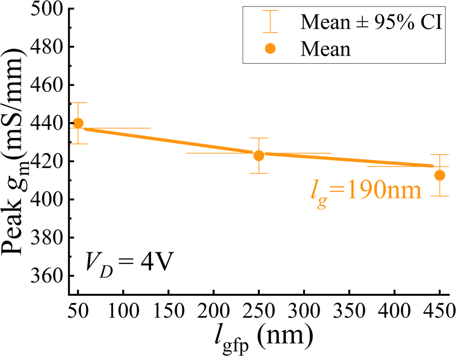
The extrinsic transconductance (gme), obtained from DC characterization, decreases with increasing the lgfp (Fig. 3). This decline is due to the larger effective gate length which results in a decline in the drain saturation current in addition to the longer lgd for larger lgfp devices [Reference Chiang, Hsu and Chang9].
Peak extrinsic transconductance for varying gate field plate lengths with error bars marking the variation across 10 measured dies at VG set to the bias corresponding to the maximum gm, and VD = 4 V. Device geometry: lg = 190 nm, lgs = 220 nm, lgd = 170 nm + lgfp, lfp (s) = 50 nm, NF × WF = 8 × 25 μm.
T-gate geometry: RF small-signal trade-offs
Measured S-parameters, using a two-port vector network analyzer (VNA), determine the small-signal device behavior. The small-signal behavior of these devices is describable by an 11-element small-signal equivalent circuit (SSEC) (Fig. 4). This modeling approach is useful for identifying possible device improvements and performance limiters; particularly since the cut-off frequencies (fT, fMAX) can be approximated from the values of the equivalent circuit [Reference Jarndal and Kompa10, Reference Alt, Marti and Bolognesi11]. fMAX can be expressed in terms of the charging time constant $\tau _{R_GC_{GD}}$ as follows:


Small-signal equivalent circuit used in the extraction of the intrinsic parameters and the extrinsic resistances after open-short de-embedding.
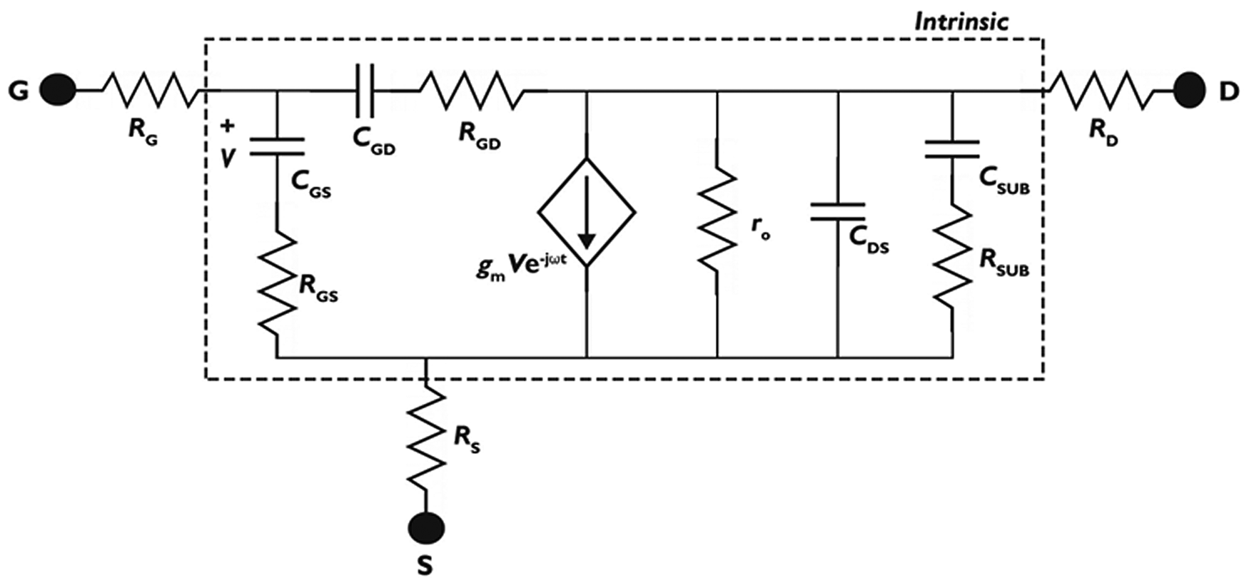
Initial estimation of the values of particular parameters in the SSEC allows for validating the extraction of the small-signal parameters from the de-embedded RF measurement data. The source and drain access resistances (RS, RD) can be calculated from the RSH and RC, where RS ,D = RSH lgs ,gd + RC. The gate resistance (RG) estimation relies on the T-gate dimensions, the gate-line sheet resistance and via resistances as detailed in [Reference ElKashlan, Rodriguez, Yadav, Khaled, Peralagu, Alian, Waldron, Zhao, Wambacq, Parvais and Collaert12]. A first-order prediction of the gate-to-source capacitance (CGS), neglecting the fringing effect, can be deduced from the gate length and barrier thickness (TBAR) using CGS = ɛlg/TBAR. Whereas the gate-to-drain capacitance (CGD) should be kept at a value below 0.3 of CGS in PA to limit the influence of the input Miller reflected capacitance in GaN HEMTs with scaled source-to-drain distances below 1 μm. The extraction of the parameter values for the SSEC follows the procedures in [Reference Jarndal and Kompa10, Reference Alt, Marti and Bolognesi11]. The final stage of extraction validation depends on comparing the SSEC S-parameters and the RF measurement data (Fig. 5). The visible kink in S 22 (Fig. 5) is an indicator of the parasitic conduction through the Si substrate, and the SSEC accounts for this effect through the RSUBCSUB branch (Fig. 4) [Reference Jarndal13, Reference Chandrasekar14]. The work in [Reference Yadav, Cardinael, Zhao, Vondkar, Khaled, Rodriguez, Vermeersch, Makovejev, Ekoga, Pottrain, Waldron, Raskin, Parvais and Collaert15, Reference Yadav, Cardinael, Zhao, Vondkar, Peralagu, Alian, Khaled, Makovejev, Ekoga, Lederer, Raskin, Parvais and Collaert16] provides further insight into the substrate-related RF losses and non-linearities for these GaN HEMTs on Si.
Measured (symbols) versus modeled (lines) S-parameters with a frequency ranging from 100 MHz to 50 GHz at VD = 4 V and VG set to maximum gm. Device geometry: lg = 190 nm, NF × WF = 8 × 25 μm, lgs = 220 nm, lgd = 170 nm + lgfp, lfp (s) = 50 nm, and lgfp = (a) 50 nm, (b) 250 nm.

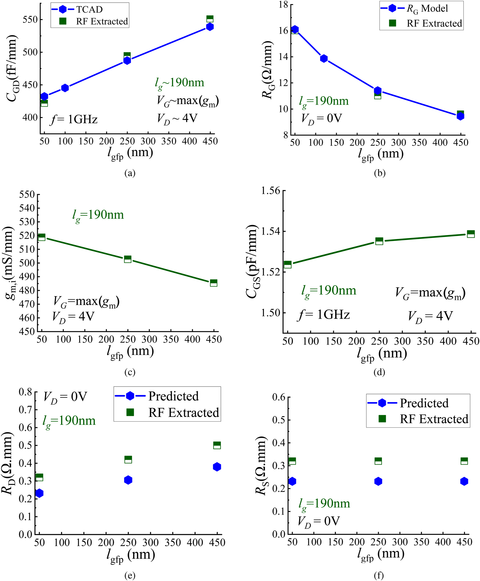
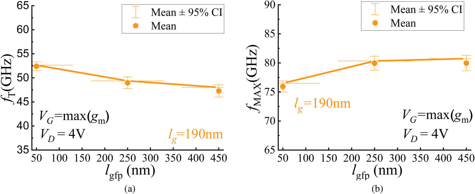
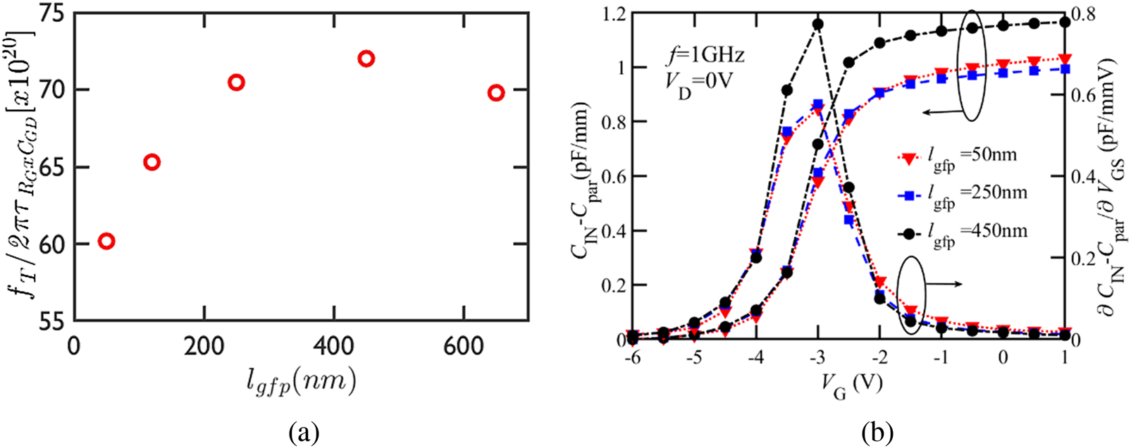
The sharp increase in RG (Fig. 6(b)) as the lgfp reduces to 50 nm causes a consequent decline in fMAX (Fig. 7(b)) even though fT (2) (Fig. 7(a)) continues to improve with smaller lgfp due to the consistent increase in the intrinsic transconductance (gmi) (Fig. 6(c)) and capacitance reduction (Figs 6(b) and 6(d)). Variation in the lgfp dimensions results in a trade-off between RG and CGD [Reference ElKashlan, Rodriguez, Yadav, Khaled, Peralagu, Alian, Waldron, Zhao, Wambacq, Parvais and Collaert12]. Assuming negligible lgfp influence on the ratio between the output and input device impedanceFootnote 1 in the formulation for fMAX, the time constant $\tau _{R_GC_{GD}}$ (Fig. 8(a)) can be used as an initial design guideline for lgfp optimization.
Extracted and predicted small-signal parameters for three different lgfp. Device geometry: lg = 190 nm, lgs = 220 nm, lgd = 170 nm + lgfp, and NF × WF = 8 × 25 μm. The remaining SSEC parameters with marginal lgfp dependence: CDS = 495 fF/mm, ro = 900 Ω/mm, and CSUB = 50 fF, RSUB = 250 Ω.
(a) fT and (b) fMAX for varying gate field plate lengths with error bars marking the variation across 10 measured dies at VG set to the bias corresponding to the maximum gm, and VD = 4 V. Device geometry: lgs = 220 nm, lgd = 170 nm + lgfp, lfp (s) = 50 nm, and NF × WF = 8 × 25 μm.
(a) The ratio between fT and the product of RG and CGD extracted from RG modeling and TCAD simulations. (b) CIN–Cparasitic, and ∂CIN/∂VGS versus VG for varying lgfp. lg = 190 nm, lgs = 220 nm, lgd = 170 nm + lgfp, and NF × WF = 8 × 25 μm.
Technology Computer-Aided Design (TCAD) device simulations performed using the Sentaurus Device software enable additional validation of the extracted CGD, where the TCAD GaN HEMT structure is generated using the Sentaurus Structure Editor software [17, 18]. The TCAD simulations include the drift-diffusion model for carrier transport and Fermi statistics. Additionally, the mobility model incorporates the doping-dependent and high-field saturation dependency. The built-in strain piezoelectric polarization model automatically computes the polarization charges at interfaces [17, Reference Ambacher, Smart, Shealy, Weimann, Chu, Murphy, Schaff, Eastman, Dimitrov, Wittmer, Stutzmann, Rieger and Hilsenbeck19]. The model coefficients have been carefully calibrated based on measurements of different GaN devices. The simulations also include the bulk and interface traps.
Using the RG model in [Reference ElKashlan, Rodriguez, Yadav, Khaled, Peralagu, Alian, Waldron, Zhao, Wambacq, Parvais and Collaert12] and the TCAD simulations to explore more lgfp geometries, it is observable that the parabolic ratio between fT and $\tau _{R_GC_{GD}}$ has an optimum beyond which its value declines. In the case of small lgfp, the decline is a result of a rise in RG, and for larger lgfp, it is a consequence of an increase in CGD coupled with a lower gm. There is no impact of lgfp variation on the RS (Fig. 6(f)). However, the direct proportionality between RD and the lgfp captures the influence of the gate-to-drain field plate (Fig. 6(e)).
As discussed in the next section, the lgfp can be optimized further for linearity; since the voltage-dependent CIN results in an amplitude-dependent phase shift which affects AM/PM. Longer lgfp exhibit a higher capacitance variation for a given VG range (∂CIN/∂VGS) (Fig. 8(b)), thereby negatively affecting the phase distortion.
Non-linear characterization
Measurement setups
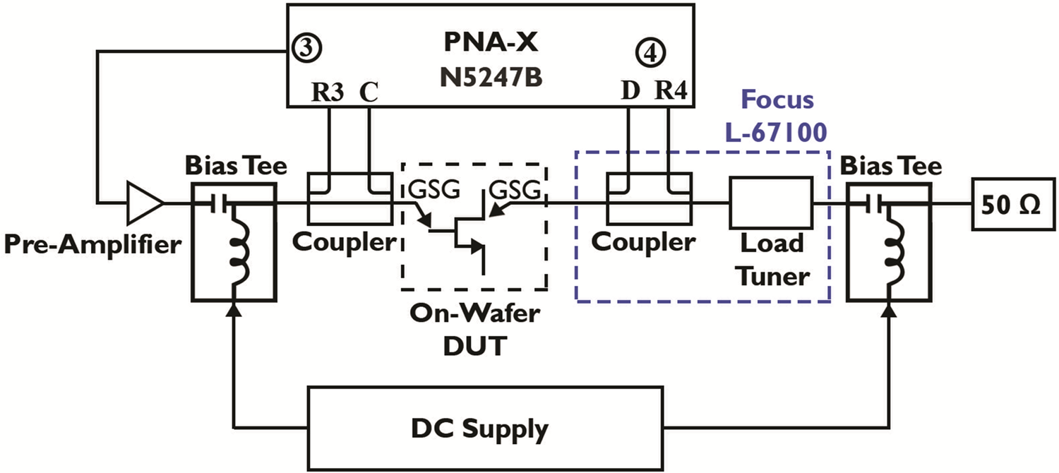
This study relies on three different setups which enable the non-linear and large-signal device characterization to examine various metrics at different fundamental frequencies. The non-linear vector network analyzer (NVNA), previously described in [Reference ElKashlan, Khaled, Rodriguez, Putcha, Peralagu, Alian, Collaert, Wambacq and Parvais6], provides non-linear device behavior insight at a fundamental frequency (f0) of 6 GHz under unmatched conditions (50 Ω) with the harmonics acquired up to 18 GHz (3f0) [Reference Betts20]. The frequency specifications of some setup components, such as the pre-amplifier and the coupler, limit the acquisition of higher-order harmonics. The matched large-signal performance of the devices is measured using passive continuous-wave load-pull setups calibrated at 6 and 28 GHz (Fig. 9). Load-pull measurements rely on controlling the reflection factor (ℾ) presented to the device, which is the ratio of the reflected power to the injected power wave into the load [Reference Tsironis21]. In passive load-pull measurements, the transmission losses and the tuner reflection capacity limit the achievable loads; hence the ℾ is always less than 1, rendering all the achievable impedances inside the smith chart. The losses of the coupler, connected between the tuner and the DUT, limit the ℾ to 0.69 (voltage standing wave ratio (VSWR) ~ 5.6) in the 6 GHz setup. In the 28 GHz load-pull measurement setup, the tuner is connected directly to the probe, thereby enabling a high ℾ of 0.891 (VSWR ~ 17.4). Rigorous calibration moves the reference plane to the tip of the 100 μm-pitch ground-signal-ground (GSG) probes. The devices are biased in the frequently preferred class AB since this class offers advantages in terms of linearity and efficiency when compared to classes B and A, respectively [Reference Cripps22]. This study considers two bias conditions; a mid-class AB bias point, consistent with the NVNA results presented in [Reference ElKashlan, Khaled, Rodriguez, Putcha, Peralagu, Alian, Collaert, Wambacq and Parvais6], at a current density of 320 mA/mm, and a deep class-AB bias at 60 mA/mm.
Passive load-pull characterization setup with the Focus L-67100 Delta Tuner. Achieved VSWR: 17.4 (ℾ: 0.891), characterization frequency f = 28 GHz.
Amplitude and phase distortion
Since GaN HEMTs show soft-compression behavior, the input power level that results in the peak power-added efficiency (PAE) and PSAT is at approximately 3 dB of compression [Reference Pedro, Nunes and Cabral23]. Hence, the maximum phase distortion reported, computed from the difference between the phase of the measured B2 and A1 waves, is at PSAT.

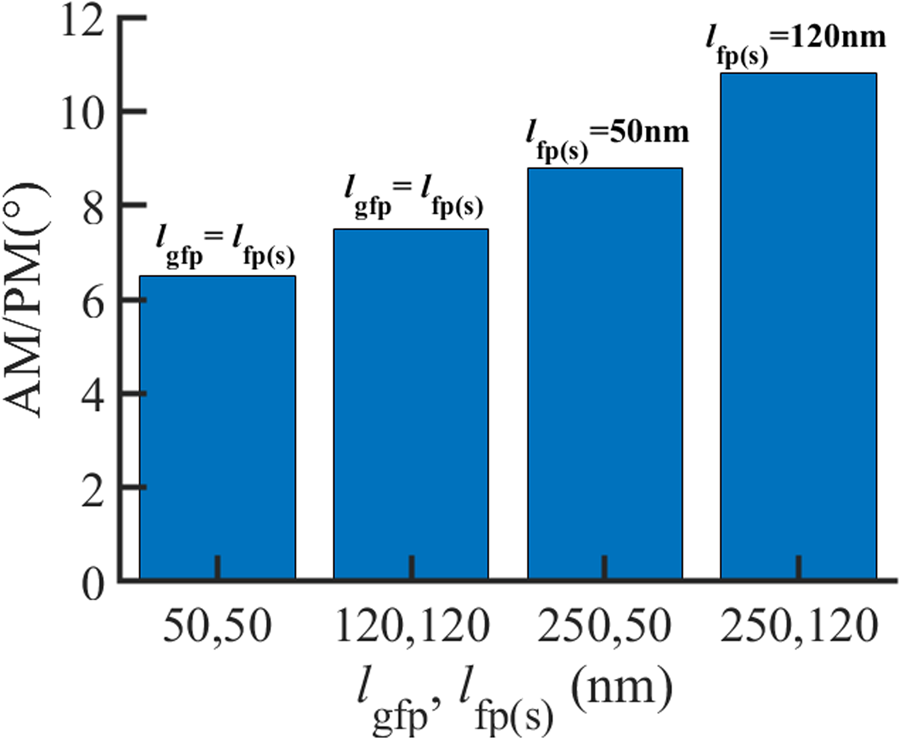
The reduction of the lgfp results in mitigation of the AM/PM (Figs 10 and 11) owing to the lower ∂CIN/∂VGS for the smallest lgfp (Fig. 8(b)) [Reference ElKashlan, Khaled, Rodriguez, Putcha, Peralagu, Alian, Collaert, Wambacq and Parvais6]. The larger the rate of change of the capacitance fluctuates for a given VG range (∂CIN/∂VGS), the higher the phase distortion [Reference Pedro, Nunes and Cabral23–Reference Khandelwal, Ghosh, Ahsan and Chauhan25]. The discussion of the impact of the matching conditions and operating frequency on the distortion will follow.
Phase distortion characteristics at 6 GHz for differing lgfp, at unmatched (NVNA) and matched (load-pull) load conditions with IDQ = 320 mA/mm and VD = 8 V. lg = 190 nm, lgs = 220 nm, lgd = 170 nm + lgfp, lfp (s) = 50 nm, and NF × WF = 8 × 25 μm.

AM/PM characteristics obtained from the 28 GHz passive load-pull characterization for varying lgfp, lfp (s) at IDQ = 60 mA/mm and VD = 4 V. lg = 190 nm, lgs = 170 nm + lfp (s), lgd = 170 nm + lgfp, and NF × WF = 8 × 12.5 μm. ZL is matched for PAE.
Although the impact of gate-to-drain capacitance (CGD) variation with the excitation amplitude on AM/PM is negligible, there is an influence of the input Miller reflected CGD on AM/PM. Such Miller capacitances are dependent on the non-linear voltage gain (Av) of the device, their loop gain (1 − Av) accordingly varies at the onset of gain compression [Reference Golara, Moloudi and Abidi26, Reference Nunes, Cabral and Pedro27].
The linearity of the transconductance profile in the region where ID is in saturation is critical at high input power levels. The gm roll-off of GaN HEMTs results in the gain compression and worsens the linearity in the PSAT regime. The non-linear access resistance is a known contributor to this gm roll-off, and its impact increases with direct proportionality to the drain current because of the rise of the electric field in the access region. Since the area below the field plate acts as a transition between the non-linear access region and the intrinsic device, it similarly influences the gm roll-off.
There is consistent direct proportionality of lgfp and AM/PM at different matching conditions (Fig. 10), operating frequencies, and bias points (Fig. 11). A 120 nm gate-to-source field plate, lfp (s), results in a 22% increase in AM/PM compared to a 50 nm lfp (s) (Fig. 11), implying that the lfp (s) has a similar impact on AM/PM as the lgfp. These findings infer that the optimal gate field plate extension lengths for linearity within the optimal range, defined in section “T-gate geometry: RF small-signal trade-offs,” are dependent on the target application. Shorter lengths are the recommended topology for phase distortion-sensitive applications at low voltage operation to maintain a sweet-spot balance of gain, AM/AM and AM/PM.
Presenting the device with a matched load raises the value of the distortion (Fig. 10). In single-stage PAs, this impact of a matched reactive load on AM/PM is linked to implicit non-linear feedback through the reverse current of the device from the drain voltage phase to the drain current phase [Reference Golara, Moloudi and Abidi26]. The need for inductive tuning for device matching is due to the capacitive nature of the device, which results in an elliptical dynamic load-line (Fig. 12(a)) [Reference Trew, Bilbro, Kuang, Liu and Yin5]. The dynamic load-line shifts and extends outside the DC IV characteristics as the device is pushed further into compression. The average RF current value also increases, which results in the commonly observed rise in ID at higher input power levels. The network capacitance rises further as the device is pushed into saturation, necessitating inductive tuning (Fig. 12(b)) for matched conditions where the device delivers peak RF performance. The change in the optimal load impedance with the operating frequency explicates the difference in AM/PM values at 6 and 28 GHz (Fig. 12(b)).
(a) Dynamic load lines, obtained from 6 GHz NVNA characterization at different compression levels, superimposed upon the DC characteristics, NF × WF = 8 × 25 μm, lgfp = lfp (s) = 50 nm, VG ranges from −6 to 0.8 V with a 0.4 V step and IDQ = 200 mA/mm, VDQ = 4 V. (b) PAE optimal load points obtained from load-pull characterization at 6 and 28 GHz for varying lgfp. lg = 190 nm.

Large-signal metrics
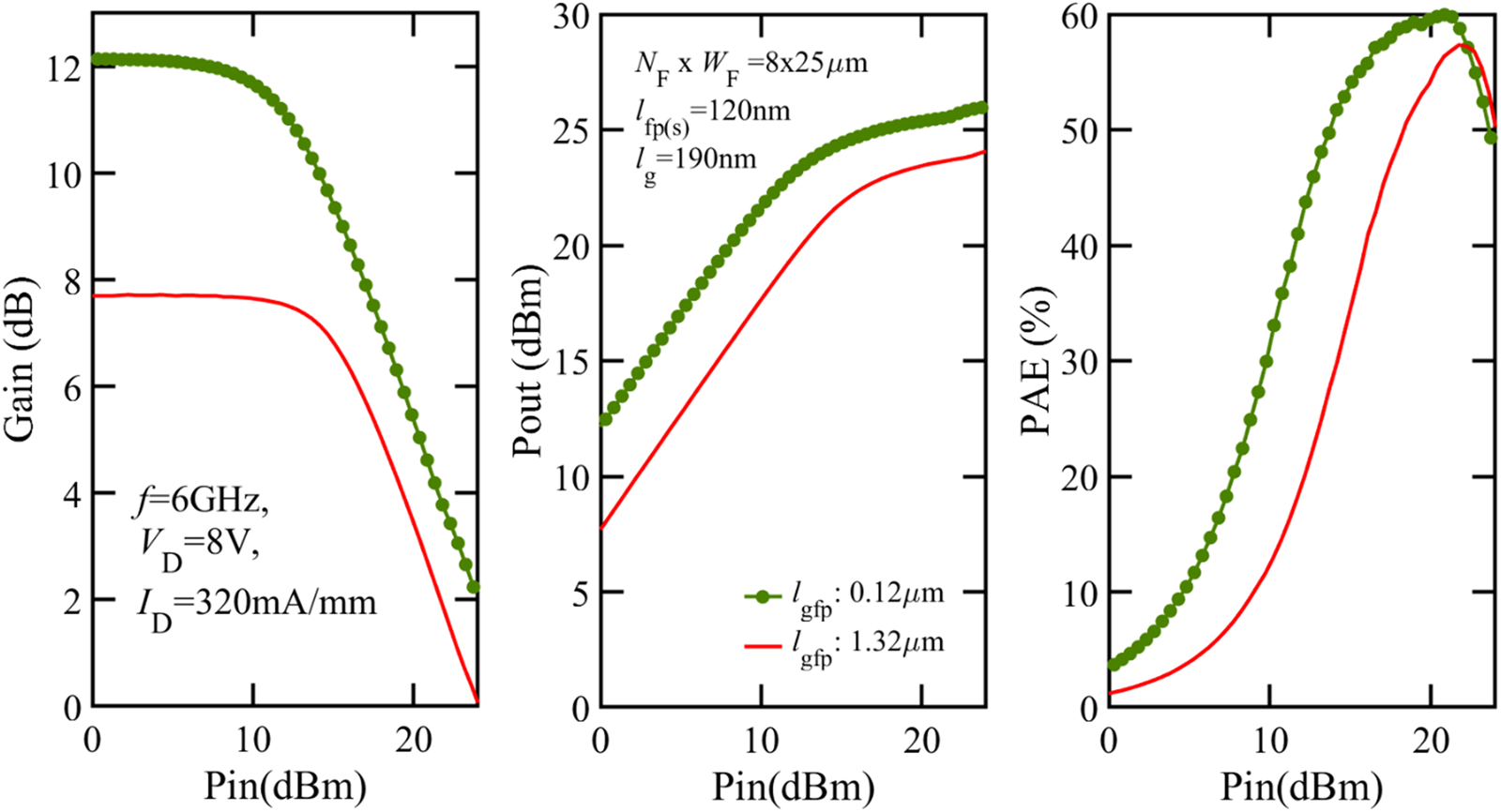
Following the gm and fT trends, the 6 GHz load-pull characterization under matched conditions for lgfp of 120 nm and 1.32 μm shows a reduction in the device power gain for the longer lgfp leading to a lower PSAT and PAE (Fig. 13). The PAE continues to improve with decreasing the lgfp until it saturates for lengths between 250 and 50 nm. The PSAT follows the same direction until it declines for a 50 nm lgfp (Fig. 14). Performing load-pull at 28 GHz leads to similar observations (Fig. 15). Varying the lfp (s) shows a decline in PAE for the longer 120 nm length. To optimize the T-gate geometry for low-voltage (VD < 10 V) mm-wave operation and considering the previous findings with regards to the device gain, AM/AM, AM/PM, and large-signal performance, the smallest feasible lgfp is the recommended choice in the range where the ratio between fT and $\tau _{R_GC_{GD}}$ does not sharply decline.
Large-signal metrics versus PIN obtained from the 6 GHz passive load-pull characterization for varying lgfp at IDQ = 320 mA/mm and VD = 8 V. lg = 190 nm, lgs = 540 nm + lfp (s), lgd = 540 nm + lgfp, lfp (s) = 120 nm, and NF × WF = 8 × 25 μm.
Median PAE, PSAT obtained from the 6 GHz passive load-pull characterization of three dies for varying lgfp at IDQ = 320 mA/mm and VD = 8 V. lg = 190 nm, lgs = 170 nm + lfp (s), lgd = 170 nm + lgfp, lgfp = 50 nm, and NF × WF = 8 × 25 μm.

Peak PAE, PSAT obtained from the 28 GHz passive load-pull characterization varying lgfp, lfp (s) at IDQ = 60 mA/mm and VD = 4 V. lg = 190 nm, lgs = 170 nm + lfp (s ), lgd = 170 nm + lgfp, and NF × WF = 8 × 12.5 μm.

Conclusion
This optimization study of T-gate geometries for linearity and improved large-signal performance indicates an optimum range for the gate field plate extension lengths for downscaled devices targeting mm-wave operation. The ratio of fT and the product of gate resistance and gate-to-drain capacitance defines this optimum, thus accounting for the sharp increase in gate resistance with aggressively downscaled gate field plates. Within that optimal range, a symmetric T-gate with a smaller gate field plate is ideal for phase distortion-sensitive applications since we find that AM/PM is inversely proportional to the gate field plate length in consequence of the direct proportionality between phase distortion and capacitance. This T-gate configuration provides the best trade-off for gain and phase linearity, thus improving the large-signal performance metrics, PAE, and PSAT.
Conflict of interest
None.
 Rana ElKashlan obtained M.Sc. in electronics and communications engineering from the American University in Cairo in 2018. She joined the Interuniversity Microelectronics Centre (imec), Leuven, Belgium, as a Ph.D. candidate in late 2019 in collaboration with the Vrije Universiteit Brussel (VUB), Brussels, Belgium. Her research focuses on the optimization of RF GaN devices for high-performance communication systems through non-linear RF characterization and modeling. She is particularly interested in a device-technology co-optimization approach for translating circuit-level requirements to device-level figures of merit.
 Ahmad Khaled obtained B.Sc. in electronics and communication from Assiut University, Egypt, in 2009. He conducted his M.Sc. research at KU Leuven/imec and graduated in 2013. He then pursued his Ph.D. in materials science engineering at the KU Leuven in the field of 3D failure analysis and graduated in 2019. Since 2018, he has been involved at imec as an R&D engineer and is currently responsible for RF device characterization in the advanced RF program at imec.
 Raul Rodriguez obtained M.Sc. in telecommunication engineering and his Ph.D. from the Universidad de Las Palmas de Gran Canaria, Las Palmas, Spain, in 2013 and 2017, respectively. He has been an R&D engineer at imec since 2018. His current research interests include electrical and thermal characterization, TCAD and modeling of Si and GaN-based devices, and the implementation of device models for circuit simulation using Verilog-A.
 Arturo Sibaja-Hernandez obtained Ph.D. in electrical engineering from the Katholieke Universiteit Leuven (KUL), Leuven, Belgium, in 2007. In 2006, he joined imec, Leuven, Belgium, where he has been focusing in the development of high speed SiGe:C HBTs, power Silicon VDMOS devices, InGaAs devices, power GaN devices, and GaN RF devices. His current research interests include supporting the development of high-frequency GaN RF devices and SACM APD devices.
 Uthayasankaran Peralagu obtained M.Eng. in electronics and electrical engineering and Ph.D. in electronics and nanoscale engineering from the University of Glasgow, Glasgow, UK, in 2008 and 2016. His M.Eng. final year thesis was on the fabrication and characterization of superconducting junctions with tailored barriers and his Ph.D. research was on the development of high-k/III-V p-channel MOSFETs for post-silicon CMOS. In 2008, he was an intern at Forschungszentrum Jülich, Jülich, Germany, where he worked on Josephson junctions. From 2013 to 2018, he was a postdoctoral associate with the University of Glasgow, where he worked on technology development for non-planar III-V CMOS for logic. In 2018, he joined Interuniversity Microelectronics Centre, Leuven, Belgium, as an R&D engineer, where he is currently working on III-N device technology and integration for advanced RF applications.
 AliReza Alian obtained his bachelor's degree in electrical engineering at the University of Tehran in 2002 and his master's degree at the Sharif University of Technology, Iran, in 2004. He received his Ph.D. in 2012 (imec/KULeuven, Belgium) on the design, fabrication, and characterization of III-V MOSFET devices. He has developed III-V logic devices as well as III-V tunnel FET devices based on GaSb and InGaAs. Since 2017 he has been working on GaN-based device design and development for RF applications at imec.
 Nadine Collaert obtained Ph.D. in electrical engineering from Katholieke Universiteit Leuven (KUL) in Belgium. She is currently the program director at imec, where she is responsible for the advanced RF program looking at heterogeneous integration of III-V/III-N devices with advanced CMOS to tackle the challenges of next-generation mobile communication. She was previously the program director of the LOGIC Beyond Si program focused on the research on novel CMOS devices and new material-enabled device and system approaches to increase functionality. She has been involved in the theory, design, and technology of FinFET devices, emerging memories, transducers for biomedical applications, and the integration and characterization of biocompatible materials. Dr. Collaert holds more than 400 publications and more than 10 patents in the field of device design and process technology.
 Piet Wambacq obtained Ph.D. in electrical engineering from the Katholieke Universiteit Leuven (KUL), Leuven, Belgium, in 1996. Since 1996, he has been with imec, Leuven, where he is currently a fellow. He is also a part-time professor with the University of Brussels (VUB), Brussels, Belgium. He authored or co-authored six books and more than 350 scientific papers. His main interests are in analog, RF, and mm-wave IC design for wireless communication and sensing applications. Dr. Wambacq has been on the Program Committee of solid-state circuit design conferences, such as European Solid-State Circuits Conference (ESSCIRC) and International Solid-State Circuits Conference (ISSCC). He was the vice-program chair of ISSCC 2022, and he is the program chair for ISSCC 2023.
 Bertrand Parvais is a principal member of the technical staff at imec, Belgium, leading the development of advanced transistors for mm-wave applications. He obtained his electrical engineering and Ph.D. degrees from the Universite Catholique de Louvain (UCL), Belgium, in 2000 and 2004, respectively. He joined imec in 2005, working in the field of transistors modeling and CMOS mm-wave/mixed-mode circuit design. He has also been a guest professor since 2017 at the Vrije Universiteit Brussel (VUB), Brussels, Belgium.


 Open access

