





Introduction
The groove gap waveguide (GGW), first introduced by Per-Simon Kildal and co-workers as a particular implementation of gap-waveguide technology, has established itself as an effective RF platform for guiding electromagnetic (EM) waves at millimeter-wave and sub-terahertz regions [Reference Kildal, Alfonso, Valero-Nogueira and Rajo-Iglesias1]. By combining low propagation loss with a mechanically robust, contactless architecture, GGW structures provide a compelling alternative to both planar transmission lines and conventional air-filled metallic waveguides, particularly in frequency regimes where fabrication tolerances and assembly complexity strongly influence RF-device performance. These advantages have recently driven significant research activity on GGW RF components, motivated by emerging RF-wireless scenarios targeting very-high regions of the radio spectrum – e.g., Beyond-5G communications supporting virtual-reality and augmented-reality applications [Reference Tataria, Shafi, Molisch, Dohler, Sjöland and Tufvesson2], and sub-terahertz imaging and sensing [Reference Mostajeran, Naghavi, Emadi, Samala, Ginsburg, Aseeri and Afshari3].
GGW operation relies on periodic metallic surfaces or lattices – typically realized using pin or ridge arrays – that emulate artificial-magnetic-conductor (AMC) EM behavior over a prescribed frequency band. When a longitudinal groove is formed between two such AMC regions and enclosed by a parallel metallic plate, the EM energy is efficiently confined within the groove. This confinement mechanism originates from the EM bandgap (EBG) produced by the surrounding periodic structures, which inhibits EM-wave propagation outside the groove without requiring electrical contact between the parallel plates. Consequently, GGW implementations can partially relax mechanical-tolerance requirements and the need for tuning features commonly used in conventional metallic waveguides, while retaining their inherent benefits of low-loss propagation and high RF-power-handling capability. These properties have enabled the successful application of GGW technology to a wide range of RF passive components operating from  $Ku$- to $W$-band frequencies, including power dividers and combiners [Reference Farahbakhsh, Zarifi and Zaman4], couplers [Reference Nasri, Zarifi and Zaman5], phase shifters [Reference Razavi and Zaman6], crossovers [Reference Farahbakhsh, Zarifi and Mrozowski7], transitions to coaxial and planar transmission lines [Reference Pérez-Guimerá, Ferrando-Rocher, Herranz-Herruzo and Valero-Nogueira8, Reference Nandi, Zaman, Vosoogh and Yang9], mode converters [Reference Wang, Wang, Cheng and Qi10], twists [Reference Zhang, Zhang, Zhou, Luo and Liu11], sensing devices [Reference Horestani, Shaterian and Mrozowski12, Reference Hosseinzadeh, Ghalibafan, Rezaee and Kheirdoost13], Butler matrices [Reference Tamayo-Domínguez, Fernández-González and Sierra-Castañer14], and antenna and antenna-array configurations including those with co-designed filtering capability [Reference Vukomanovic, Vázquez-Roy, Quevedo-Teruel, Rajo-Iglesias and Sipus15–Reference Zhang, Gu, Ni, Yu, Liu, Zhou, Yang and Hong19].
In comparison, the development of frequency-selective RF circuits based on GGW technology has progressed more slowly. Nevertheless, particularly over the last few years, notable research efforts have been dedicated to the realization of GGW RF filtering components. Representative examples are reported in [Reference Vague, Asensio, Coves, San Blas, Reglero, Vidal-Pantaleoni, Raboso, Baquero-Escudero and Boria20–Reference Reuter, Boe, Miek, Höft, Studnitzky, Zhong, Weißgärber and Olaya-Leon38]. These GGW RF devices consist of bandpass filters (BPFs) using different operational principles and schemes for designs covering various spectral regions in the millimeter-to-sub-millimeter-wave ranges, including the  $Ku$,
$Ku$,  $Ka$,
$Ka$,  $V$,
$V$,  $W$,
$W$,  $E$, and $D$ bands. Some early GGW BPF developments employ simple in-line configurations with limited selectivity, primarily serving as technology demonstrators to explore additional RF performance aspects, such as high-power effects – including passive inter-modulation, multi-pactor, and corona-discharge breakdown – to examine their use in satellite communications [Reference Vague, Asensio, Coves, San Blas, Reglero, Vidal-Pantaleoni, Raboso, Baquero-Escudero and Boria20, Reference Morales-Hernández, Sánchez-Soriano, Ferrando-Rocher, Marini and Boria21]. More-advanced realizations, however, feature sharp-rejection filtering responses with out-of-band transmission zeros (TZs) at both passband sides. These high-selectivity RF BPFs with stopband TZs are designed either through cross-coupled GGW-cavity-resonator networks implemented in single- and multi-layer architectures – e.g., [Reference Al-Juboori, Huang, Klugmann, Hussein and Zhou25, Reference Xiu, Yao, Jiang, Cheng, Wang, Wang, Yu and Chen28] – or by means of in-line BPF topologies incorporating dedicated multi-TZ-generation mechanisms, such as frequency-dependent $/$variant couplings contributing with TZs and even in-band poles in some particular realizations, GGW cavities with loaded stubs, or oversized GGW cavities acting as reactive loads connected at the input of low-selectivity GGW BPF units – e.g., [Reference Miek, Boe, Kamrath and Höft26, Reference Malki, Yang and Gómez-García27]. To a lesser extent, congregations of two RF BPFs to form diplexers in GGW have also been demonstrated, ranging from designs with widely spaced channels and reduced near-passband selectivity as in [Reference Rezaee, Zaman and Kildal39, Reference Marini, Ferrando-Rocher, Morales-Hernández, Gimeno-Nieves, López and Boria40] to more-challenging contiguous-channel RF diplexers exhibiting ultra-abrupt cut-off slopes as in [Reference Malki and Gómez-García41]. In addition, only a limited number of studies have addressed alternative filtering responses in GGW realizations, such as quasi-lowpass filters [Reference Santiago, Laso, Lopetegi and Arregui42], further confirming the suitability of emerging selective-laser-melting- (SLM) 3-D printing techniques for this RF technology.
The case of highly selective GGW RF multi-band BPFs remains comparatively underexplored, with only a very few dual-passband solutions reported to date [Reference Malki, Yang and Gómez-García29, Reference Huang, Zhang, Zhou, Lu, Tam, Zhang and Tang43–Reference Malki, Yang and Gómez-García45]. However, these designs suffer from one or more shortcomings, as follows: absence of adjacent-to-passband TZs at both sides of the two transmission bands, increased structural complexity and sensitivity due to the need for multi-mode resonators and $/$or cross-coupling mechanisms for out-of-band TZ generation, or large physical size $/$volume.
In this paper, an original class of GGW sharp-rejection multi-band BPFs is proposed. This type of filter incorporates stopband TZs on both sides of all passbands, enabling steep out-of-band attenuation without requiring cross-coupling mechanisms in fully inductive-coupling filter architectures. This RF behavior is achieved by employing dedicated input and output feeding sections, each loaded with a pair of dangling tails formed by  $M$ GGW rectangular cavities for an $M$-passband design, in combination with an in-line split-type $M$-band BPF block. The resulting multi-extracted-cavity GGW multi-band BPF is obtained from an initial single-band prototype featuring two close-to-passband TZs through the application of a split-type single-to-multi-band frequency transformation.
An earlier version of this paper was presented at the 55th European Microwave Conference (EuMC 2025) and was published in its Proceedings [Reference Malki and Gómez-García46]. The present paper significantly extends the referred initial article with the following additional contents: (i) generalization of the theoretical framework from dual- to  $M$-band designs with their corresponding theoretical synthesis examples at the coupling-routing-diagram level – namely, fourth-order dual-band and sixth-order triple-band examples, (ii) sensitivity analyses of the developed GGW dual-band BPF to assess fabrication robustness, and (iii) quantitative evaluation of RF performance merits with respect to the state-of-the-art through a comprehensive comparison table.
The remainder of the manuscript is organized as follows: in the Theoretical foundations section, the RF operational foundations of the engineered approach of multi-band BPF using the coupling-routing-diagram formalism are detailed, including theoretical design examples of multi-band bandpass filtering responses with spectrally symmetrical and asymmetrical profiles. The design of the core GGW to be employed in the subsequent practical development of dual-band BPF is also presented. In the Experimental results section, a proof-of-concept prototype of 14 $/$14.4-GHz fourth-order dual-band BPF implemented in a two-layer-vertically stacked GGW structure is manufactured and tested for experimental-validation purposes. Sensitivity analyses of this GGW dual-band BPF circuit and a detailed comparison with prior-art GGW filtering devices are also reported in this section. Finally, the main concluding remarks of this work are set out in the Conclusion section.
Theoretical foundations
Coupling-routing diagram and design examples
The generalized normalized coupling-routing diagrams of the proposed dual- and triple-band BPF networks together with their single-band prototype counterpart for  $N$th-order architectures are depicted in Figure 1. As shown, the baseline single-band prototype is formed by $N-2$ resonating nodes in an in-line topology with its respective input and output feeding sections. Each feeding section comprises a zero-susceptance non-resonating node with two dangling resonating nodes directly coupled to it. These input and output feeding sections contribute two out-of-band TZs at the natural frequencies of their dangling resonating nodes to the overall filtering response – i.e., at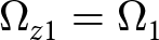 $\Omega_{z1}=\Omega_1$ and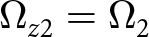 $\Omega_{z2}=\Omega_2$ and at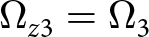 $\Omega_{z3}=\Omega_3$ and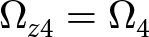 $\Omega_{z4}=\Omega_4$ for the input and output feeding sections, respectively – by creating a short circuit in the in-line path at these frequencies, as well as one pole located between the two TZs. The formulas for the normalized frequencies of these poles corresponding to the input and output feeding sections, $\Omega_{pS}$ and $\Omega_{pL}$, respectively, which are obtained by imposing the mutual cancellation of the equivalent normalized admittances of their two constituent dangling branches, are as follows:
 \begin{equation}
\Omega_{pS}=\frac{M_{S,N-1}\Omega_2+M_{S,N}\Omega_1}{M_{S,N-1}^2+M_{S,N}^2}
\end{equation}
\begin{equation}
\Omega_{pS}=\frac{M_{S,N-1}\Omega_2+M_{S,N}\Omega_1}{M_{S,N-1}^2+M_{S,N}^2}
\end{equation} \begin{equation}
\Omega_{pL}=\frac{M_{N+1,L}\Omega_4+M_{N+2,L}\Omega_3}{M_{N+1,L}^2+M_{N+2,L}^2}.
\end{equation}
\begin{equation}
\Omega_{pL}=\frac{M_{N+1,L}\Omega_4+M_{N+2,L}\Omega_3}{M_{N+1,L}^2+M_{N+2,L}^2}.
\end{equation}Normalized coupling-routing diagrams for  $N$th-order realizations of the dual- and triple-band BPF networks and its initial single-band prototype counterpart to which the frequency transformations $\Omega \rightarrow \mathcal{F}_{M=2}\left(\Omega \right)$ in (3) and $\Omega \rightarrow \mathcal{F}_{M=3}\left(\Omega \right)$ and (4), respectively, are applied (black circles: resonating nodes with normalized natural frequencies $\Omega_0,\Omega_1,\Omega_2,\Omega_3,\Omega_4,\Omega_0+\Omega_A,\Omega_1+\Omega_A,\Omega_2+\Omega_A,\Omega_3+\Omega_A,\Omega_4+\Omega_A,$ $\Omega_B,$ and $\Omega_C$; white circles: unitary source [S] and load [L]; continuous lines: couplings; $M$,
$M$,  $\alpha_{1},$ and $\alpha_{2}$ variables: normalized coupling coefficients or inversion constants of the normalized admittance inverters;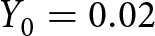 $Y_0 = 0.02$ $\mho$: reference $/$port admittance).

Figure 1 Long description
The diagram consists of three sections representing different bandpass filter (BPF) configurations. The top section illustrates a triple-band BPF with resonating nodes and coupling lines. Black circles represent resonating nodes with normalized natural frequencies, while white circles denote unitary source (S) and load (L). Continuous lines indicate couplings. The nodes are labeled with variables such as Omega subscript zero, Omega subscript one and so on, indicating normalized frequencies. The middle section shows a single-band BPF, with a similar arrangement of nodes and couplings, but fewer in number. The bottom section depicts a dual-band BPF, again with resonating nodes and couplings, but with a different configuration from the triple-band BPF. Each section is connected by transformations indicated by arrows labeled with Omega to F subscript M equals two left parenthesis Omega right parenthesis and Omega to F subscript M equals three left parenthesis Omega right parenthesis. The diagram includes labels for coupling coefficients and inversion constants, such as alpha subscript one and alpha subscript two and reference port admittance Y subscript zero equals zero point zero two. The layout shows the progression from a single-band prototype to dual- and triple-band configurations through frequency transformations.
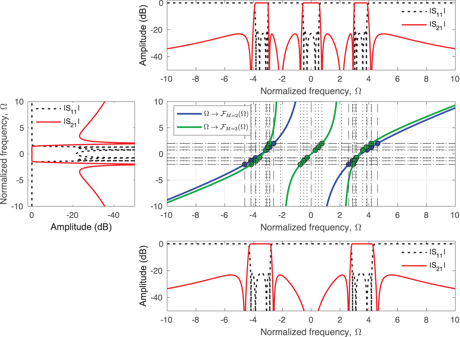
Effect of the normalized-frequency transformations  $\Omega \rightarrow \mathcal{F}_{M=2}\left(\Omega \right)$ in (3) and $\Omega \rightarrow \mathcal{F}_{M=3}\left(\Omega \right)$ in (4) in terms of power transmission $(|S_{21}|)$ and input-reflection $(|S_{11}|)$ responses – i.e., from single-band prototype to dual- and triple-band BPFs, respectively – using the normalized coupling-routing diagrams in Figure 1 for fourth-order realizations – i.e., $N=4$; dual-band BPF: $\alpha_{1}=3.464$; triple-band BPF: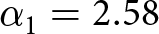 $\alpha_{1}=2.58$ and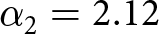 $\alpha_{2}=2.12$; $M_{S,1} = M_{S,3} = M_{S,4} = M_{2,L} = M_{5,L} = M_{6,L} = 1$,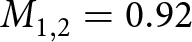 $M_{1,2} = 0.92$, $\Omega_0 =$ $\Omega_A =$ $\Omega_B =$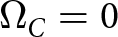 $\Omega_C = 0$, and $\Omega_1=-\Omega_2 = \Omega_3=-\Omega_4 = -2$ in both cases.
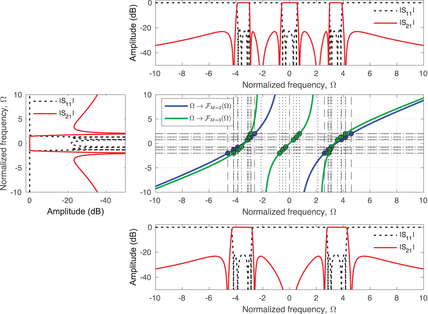
Figure 2 Long description
A composite figure with four sub-images. The image A showing a line graph with y-axis label “Amplitude (dB)” and x-axis label “Normalized frequency, Omega”. The x-axis ranges from minus 10 to 10 with ticks at minus 10, minus 8, minus 6, minus 4, minus 2, 0, 2, 4, 6, 8, 10. The y-axis shows ticks at 0, minus 20, minus 40. A legend at upper right shows a dashed black curve labeled “vertical bar S subscript 11 vertical bar” and a solid curve labeled “vertical bar S subscript 21 vertical bar”. The dashed curve is near 0 across the plot, with multiple narrow downward dips clustered between about minus 4 and plus 4. The solid curve forms three flat-topped regions near 0 centered around approximately minus 3, 0 and plus 3, separated by deep narrow notches; outside these regions it slopes downward toward about minus 40 near the ends. The image B showing a line graph with y-axis label “Normalized frequency, Omega” and x-axis label “Amplitude (dB)”. The y-axis ranges from minus 10 to 10 with ticks at minus 10, minus 5, 0, 5, 10. The x-axis shows ticks at 0, minus 20, minus 40. A legend at upper left shows a dashed black curve labeled “vertical bar S subscript 11 vertical bar” and a solid curve labeled “vertical bar S subscript 21 vertical bar”. The dashed curve is near 0 with a band of oscillating dips between about minus 20 and minus 40 over a vertical span around Omega near 0. The solid curve forms a wide shape around Omega near 0 with a near-vertical segment close to amplitude 0 and two outward bulges reaching toward about minus 40 at Omega near plus 10 and Omega near minus 10. The image C showing a line graph with y-axis unlabeled and x-axis label “Normalized frequency, Omega”. The x-axis ranges from minus 10 to 10 with ticks at minus 10, minus 8, minus 6, minus 4, minus 2, 0, 2, 4, 6, 8, 10. The y-axis ranges from minus 10 to 10 with ticks at minus 10, minus 5, 0, 5, 10. A legend at upper left shows two curves: “Omega arrow F subscript M equals 2 left parenthesis Omega right parenthesis” and “Omega arrow F subscript M equals 3 left parenthesis Omega right parenthesis”. Two smooth increasing curves run from lower left to upper right, one above the other in parts, with several circular markers placed along the curves. Multiple vertical dashed guide lines appear in three clusters centered near Omega about minus 3, 0 and plus 3 and several horizontal dashed guide lines appear around y values near 0. The image D showing a line graph with y-axis label “Amplitude (dB)” and x-axis label “Normalized frequency, Omega”. The x-axis ranges from minus 10 to 10 with ticks at minus 10, minus 8, minus 6, minus 4, minus 2, 0, 2, 4, 6, 8, 10. The y-axis shows ticks at 0, minus 20, minus 40. A legend at upper right shows a dashed black curve labeled “vertical bar S subscript 11 vertical bar” and a solid curve labeled “vertical bar S subscript 21 vertical bar”. The dashed curve is near 0 with multiple narrow dips concentrated between about minus 4 and plus 4. The solid curve has two flat-topped regions near 0 centered around approximately minus 3 and plus 3, with deep narrow notches near the edges of these regions and a broad low region around Omega near 0 reaching below minus 40.
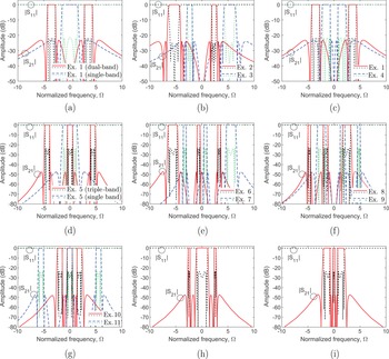
Power transmission ( $|S_{21}|$) and input-reflection ( $|S_{11}|$) responses of frequency-symmetrical and asymmetrical theoretical design examples of the normalized coupling-routing diagrams of the dual- and triple-band BPFs in Figure 1 for fourth- and sixth-order realizations – i.e., $N=4$ and $6$, respectively – together with the $|S_{21}|$ and $|S_{11}|$ responses of its initial single-band prototype counterpart in the frequency-symmetrical cases. (a) Example 1: $M_{S,1} = M_{S,3} = M_{S,4} = M_{2,L} = M_{5,L} = M_{6,L} = 1$,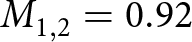 $M_{1,2} = 0.92$,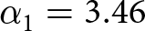 $\alpha_{1}=3.46$, $\Omega_0 = \Omega_A = \Omega_B = 0$, and $\Omega_1=-\Omega_2 = \Omega_3=-\Omega_4 = -2$. (b) Examples 2 (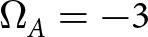 $\Omega_A = -3$) and 3 (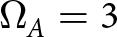 $\Omega_A = 3$): $M_{S,1} = M_{S,3} = M_{S,4} = M_{1,2}= M_{2,L} = M_{5,L} = M_{6,L} = 1$,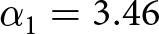 $\alpha_{1}=3.46$, $\Omega_0 = \Omega_B = 0$, $\Omega_1=-\Omega_2 = -2$, and $\Omega_3=-\Omega_4 = -2.75$. (c) Examples 4: $M_{S,1} = M_{S,3} = M_{S,4} = M_{2,L} = M_{5,L} = M_{6,L} = 1$,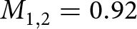 $M_{1,2} = 0.92$, $\alpha_{1}=1.304$, $\Omega_0 = \Omega_A = \Omega_B = 0$, and $\Omega_1=-\Omega_2 = \Omega_3=-\Omega_4 = -2$. (d) Example 5: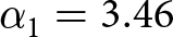 $\alpha_{1}=3.46$, $\alpha_2=2.574$, $\Omega_0=$ $\Omega_A=$ $\Omega_B=$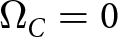 $\Omega_C=0$, and $\Omega_1=$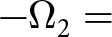 $-\Omega_2=$ $\Omega_3=$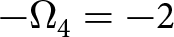 $-\Omega_4=-2$. (e) Examples 6 (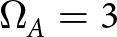 $\Omega_A=3$) and 7 (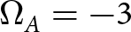 $\Omega_A=-3$): $\alpha_{1}=3.464$, $\alpha_2=2.034$, $\Omega_0=$ $\Omega_B=$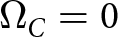 $\Omega_C=0$, and $\Omega_1=$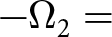 $-\Omega_2=$ $\Omega_3=$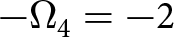 $-\Omega_4=-2$. (f) Examples 8 (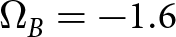 $\Omega_B=-1.6$ and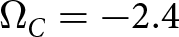 $\Omega_C=-2.4$) and 9 (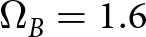 $\Omega_B=1.6$ and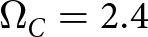 $\Omega_C=2.4$): $\alpha_{1}=2.664$, $\alpha_2=1.914$, $\Omega_0=$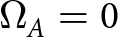 $\Omega_A=0$, and $\Omega_1=$ $-\Omega_2$ = $\Omega_3=$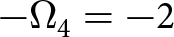 $-\Omega_4=-2$. (g) Examples 10 ( $\alpha_{1}=1.304$ and $\alpha_{2}=1.074$) and 11 ( $\alpha_{1}=4.424$ and $\alpha_2=3.174$): $\Omega_0=$ $\Omega_A$ = $\Omega_B$ =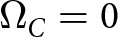 $\Omega_C=0$, $\Omega_1=-\Omega_2 = \Omega_3=-\Omega_4 = -2$. Examples (h) ( $\alpha_{2}=2.154$) and (i) ( $\alpha_{2}=0.414$): $\alpha_{1}=1.064$, $\Omega_0$ = $\Omega_A$ = $\Omega_B$ =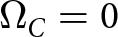 $\Omega_C=0$, $\Omega_1=-\Omega_2 = \Omega_3=-\Omega_4 = -2$; $M_{S,1} = M_{4,L}=0.94$, $M_{S,5} = M_{S,6} = M_{7,L} = M_{8,L} = 1$, $M_{1,2}=M_{3,4}=0.81$, and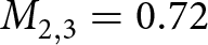 $M_{2,3}=0.72$ for all triple-band BPF examples in (d)–(i).

Figure 3 Long description
The plots illustrate magnitude responses of multi-band filters versus normalized frequency, omega, in various design examples. The vertical axis is labeled amplitude in decibels, ranging from 0 to minus 80. The horizontal axis is normalized frequency, omega, ranging from minus 10 to 10. The variables vertical bar S subscript 11 vertical bar and vertical bar S subscript 21 vertical bar represent reflection and transmission responses, respectively. In (a), dual-band and single-band examples show passbands near omega equals minus 3 and 3, with stopbands reaching minus 50 decibels. In (b), examples 2 and 3 display multiple passbands with deep notches, indicating strong attenuation. In (c), example 1 and 4 show similar passband locations with variations in stopband depth. In (d), triple-band and single-band examples exhibit passbands around omega equals minus 3, 0 and 3, with stopbands reaching minus 80 decibels. In (e), examples 6 and 7 demonstrate similar passband structures with differing notch placements. In (f), examples 8 and 9 highlight variations in passband bandwidths and stopband depths. In (g), examples 10 and 11 show distinct passband separations and notch depths. In (h) and (i), the plots illustrate consistent passband locations with variations in stopband attenuation. Overall, the plots compare the performance of different filter designs, highlighting differences in passband locations, bandwidths and stopband attenuation.
Consequently, the resulting single-band filtering response exhibits up to  $N$ in-band reflection zeros (RZs) and up to four finite-frequency stopband TZs at distinct spectral locations – which may be grouped in pairs to yield double-multiplicity TZs, i.e.,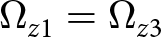 $\Omega_{z1}=\Omega_{z3}$ and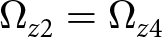 $\Omega_{z2}=\Omega_{z4}$ – without the need for cross-coupling mechanisms in the single-band prototype.
The dual- and triple-band BPFs are derived by applying split-type single-to-dual-band and single-to-triple-band frequency transformations,  $\Omega \rightarrow \mathcal{F}_{M=2}(\Omega)$ and $\Omega \rightarrow \mathcal{F}_{M=3}(\Omega)$, respectively, to the initial single-band prototype in the normalized domain. The analytical expressions of these frequency transformations are as follows:
 \begin{equation}
\mathcal{F}_{M=2}(\Omega)
=
\Omega - \Omega_A
-
\dfrac{\alpha_1^2}{
\Omega - \Omega_B
}
\end{equation}
\begin{equation}
\mathcal{F}_{M=2}(\Omega)
=
\Omega - \Omega_A
-
\dfrac{\alpha_1^2}{
\Omega - \Omega_B
}
\end{equation} \begin{equation}
\mathcal{F}_{M=3}(\Omega) =
\Omega - \Omega_A
-
\dfrac{\alpha_1^2}{
\Omega - \Omega_B
-
\dfrac{\alpha_2^2}{
\Omega - \Omega_C
}}
\end{equation}
\begin{equation}
\mathcal{F}_{M=3}(\Omega) =
\Omega - \Omega_A
-
\dfrac{\alpha_1^2}{
\Omega - \Omega_B
-
\dfrac{\alpha_2^2}{
\Omega - \Omega_C
}}
\end{equation} where  $\Omega_A,\Omega_B, \Omega_C,\alpha_{1}$, and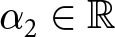 $\alpha_{2}\in \mathbb{R}$. Due to these frequency transformations, additional resonating nodes appear coupled to each resonating node of the single-band prototype – namely, one and two extra resonating nodes for the dual- and triple-band cases, respectively. This equivalently results in the frequency mapping of the single-band prototype response into dual- and triple-band responses with up to five and eight distinct finite-frequency stopband TZs, respectively. The middle TZ(s) between passbands have multiplicity $N-2$ and come from the TZ at $\pm\infty$ of the core single-band prototype after frequency transformation. The TZs closer to the passbands come from their counterparts in the baseline single-band prototype after frequency mapping. Furthermore, the in-band characteristics of the single-band prototype are preserved and transferred to the passbands of the dual- and triple-band BPF responses in terms of filter order and input-power-matching profile. Note that the frequency transformations in (3) and (4) correspond to the particular cases of the generalized split-type single-to- $M$-band frequency transformation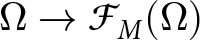 $\Omega \rightarrow \mathcal{F}_{M}(\Omega)$ in (5) for $M=2$ – dual-band response – and $M=3$ – triple-band response – with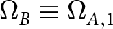 $\Omega_B\equiv\Omega_{A,1}$ and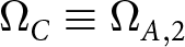 $\Omega_C\equiv\Omega_{A,2}$ for notation simplicity.
 \begin{align}
& \Omega \;\longrightarrow\; \mathcal{F}_M(\Omega)\nonumber\\
& \quad= \Omega - \Omega_A - \dfrac{\alpha_1^2}{ \Omega - \Omega_{A,1} - \dfrac{\alpha_2^2}{\Omega - \Omega_{A,2} - \dfrac{\alpha_3^2}{\ddots - \dfrac{\alpha_{M-1}^2}{\Omega - \Omega_{A,M-1}}}}}
\end{align}
\begin{align}
& \Omega \;\longrightarrow\; \mathcal{F}_M(\Omega)\nonumber\\
& \quad= \Omega - \Omega_A - \dfrac{\alpha_1^2}{ \Omega - \Omega_{A,1} - \dfrac{\alpha_2^2}{\Omega - \Omega_{A,2} - \dfrac{\alpha_3^2}{\ddots - \dfrac{\alpha_{M-1}^2}{\Omega - \Omega_{A,M-1}}}}}
\end{align} For illustrative purposes, Figure 2 presents examples of the theoretical power transmission and input-reflection responses for the dual- and triple-band BPF cases to show the effect of the normalized-frequency transformations in (3) and (4), respectively. As observed, the sharp-rejection transmission band of the initial single-band prototype employing input $/$output extracted cavities in Figure 1 is split into two and three narrower passbands for the dual- and triple-band cases, respectively. All resonating nodes contribute equally to shaping these transmission bands. Simultaneously, five and eight stopband TZs are obtained in the dual- and triple-band responses, with trios of TZs located between passbands and additional TZs appearing below the lowest and above the highest passbands. In particular, the spectral locations of these TZs closest to the passbands are determined by their homologous counterparts in the initial single-band prototype in Figure 1, and by the parameters $\alpha_{1}$ and $\alpha_{2}$ of the frequency transformations. Consequently, the steep-selectivity characteristics of the original single-band response are retained in the resulting dual- and triple-band BPF networks, along with the pre-designed minimum in-band power-matching level of 21.5 dB for all transmission bands, each exhibiting equirriple-type in-band behavior.
For 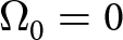 $\Omega_0=0$ – i.e., normalized single-band prototype in Figure 1 centered at $\Omega=0$ – the normalized center frequencies of the passbands of the $M$-band BPF derived from the frequency transformation in (5) can be obtained as follows:
 \begin{equation}
\left.\mathcal{F}_{M}(\Omega)\right|_{\Omega_{01},\Omega_{02},\ldots,\Omega_{0M}}=0
\end{equation}
\begin{equation}
\left.\mathcal{F}_{M}(\Omega)\right|_{\Omega_{01},\Omega_{02},\ldots,\Omega_{0M}}=0
\end{equation}where  $\Omega_{01} \lt \Omega_{02} \lt \cdots \lt \Omega_{0M}$ denote the normalized center frequencies from the lowest to the highest passband. Their formulas for the resulting dual-, triple-, and quadruple-band responses – i.e.,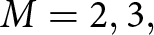 $M=2,3,$ and $4$ – assuming that $\Omega_{A,1}=\Omega_{A,2}=\Omega_{A,3}=0$ for simplicity, which are frequency symmetrical with regard to $\Omega=0$, are given below.
• Dual-band BPF – i.e., $M=2$:

 \begin{equation}
\Omega_{01},\Omega_{02}= \pm |\alpha_1|.
\end{equation}
\begin{equation}
\Omega_{01},\Omega_{02}= \pm |\alpha_1|.
\end{equation}• Triple-band BPF – i.e.,
$M=3$:

 \begin{equation}
\Omega_{01},\Omega_{03}= \pm \sqrt{\alpha_1^2+\alpha_2^2} \qquad \Omega_{02} = 0.
\end{equation}
\begin{equation}
\Omega_{01},\Omega_{03}= \pm \sqrt{\alpha_1^2+\alpha_2^2} \qquad \Omega_{02} = 0.
\end{equation}• Quadruple-band BPF – i.e.,
$M=4$:

 \begin{gather}\Omega_{01},\Omega_{02},\Omega_{03},\Omega_{04}= \cr \pm\sqrt{\frac{\alpha_1^2+\alpha_2^2+\alpha_3^2\pm\sqrt{\left(\alpha_1^2+\alpha_2^2+\alpha_3^2\right)^2-4\alpha_1^2\alpha_3^2}}{2}}.\end{gather}
 As demonstration, various theoretical design examples are presented in Figure 3, illustrating the power-transmission and input-reflection responses associated with the normalized coupling-routing diagrams of the dual- and triple-band BPF networks in Figure 1 for fourth- and sixth-order – i.e.,  $N = 4$ and $6$ – schemes, respectively. All examples have in-band input-power-matching levels above 21.5 dB. Specifically, Figure 3(a) shows a frequency-symmetrical dual-band BPF with four in-band RZs and five distinct out-of-band TZs, along with its baseline single-band prototype. Two examples of spectrally asymmetrical dual-band BPFs exhibiting three in-band RZs and nine out-of-band TZs at nonuniform finite frequencies are depicted in Figure 3(b). On the other hand, Figure 3(c) shows the flexibility to control the frequency spacing between the two passbands by simply adjusting $\alpha_{1}$, which defines the coupling between the extra resonators owing the single-to-dual-band frequency transformation and the resonating nodes of the initial single-band prototype; particularly, a stronger coupling $\alpha_{1}$ leads to a wider inter-passband separation, and vice versa. Additionally, Figure 3(d)–(i) illustrates the sixth-order triple-band BPF case. As in the fourth-order dual-band BPFs, the obtained responses reveal high degree of design versatility. Specifically, asymmetric-passband configurations can be synthesized, in which two transmission bands exhibit identical bandwidths while the third one differs (Figure 3(e)). Moreover, fully independent control of the three passband bandwidths is also achievable (Figure 3(f)). In both cases – Figure 3(e) and (f) – the locations of the center frequencies of the passbands and out-of-band TZs remain adjustable. In addition, the spacing between adjacent passbands can be reduced or increased by just tuning the coupling between the extra resonators and the resonating nodes of the initial single-band prototype – i.e., $\alpha_{2}$ – (Figure 3(g)). Finally, further flexibility is obtained by enabling either independent or simultaneous control of the bandwidths of all three passbands without modifying their center frequencies or stopband TZ positions, as illustrated in Figure 3(h) and (i).
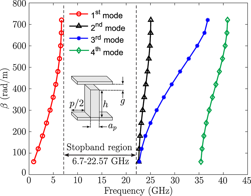
Dispersion diagram of the GGW and dimensions of the constituent pin ( $h=6.475$ mm,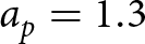 $a_{p}=1.3$ mm,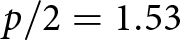 $p/2=1.53$ mm, and $g=0.125$ mm).

Figure 4 Long description
Beta (rad/m) A line graph with four plotted mode curves and an inset schematic. The x-axis is labeled Frequency (GHz), ranging from 0 to 45 with tick marks at 0, 5, 10, 15, 20, 25, 30, 35, 40 and 45. The y-axis is labeled beta (rad/m), ranging from 0 to 800 with tick marks at 0, 100, 200, 300, 400, 500, 600, 700 and 800. A legend in the upper right lists: 1st mode, 2nd mode, 3rd mode, 4th mode. 1st mode (red circles): a rising curve from about (5, 0) to about (10, 700). 2nd mode (black triangles): a rising curve from about (22.5, 0) to about (25, 700). 3rd mode (blue diamonds): a rising curve from about (25, 0) to about (35, 700). 4th mode (green diamonds): a rising curve from about (35, 0) to about (40, 700). Text near the lower middle reads: Stopband region 6.7-22.57 GHz. Inset schematic: a small diagram shows a vertical pin-like shape above a base. Dimension arrows are labeled p over 2, h, g and a subscript p.
Core GGW
Since the GGW multi-extracted-cavity dual-band BPF prototype later introduced in the Experimental results section is developed for Ku-band operation, the careful selection of the periodic pin surface that forms the GGW core is essential. The geometrical parameters of the metallic pins to be employed in the referred filter design are detailed in the caption of Figure 4. This figure presents the dispersion characteristics of the periodic structure, which were computed using the full-wave EM solver CST Studio Suite. The analyzed pin array exhibits the properties of an AMC, preventing EM-field propagation over a defined frequency interval due to the presence of an EBG. As can be observed from the dispersion diagram in Figure 4, the forbidden EM-propagation band spans from 6.7 to 22.57 GHz, thereby fully encompassing the Ku band. Consequently, this periodic-pin-lattice configuration effectively suppresses unwanted parallel-plate modes within the operational frequency range, ensuring a proper GGW behavior and making the proposed pin geometry well suited for the intended Ku-band dual-band filter realization – whose lower and upper passbands are specified to be centered at 14 and 14.4 GHz, respectively.
Experimental results
Fabrication and measurement
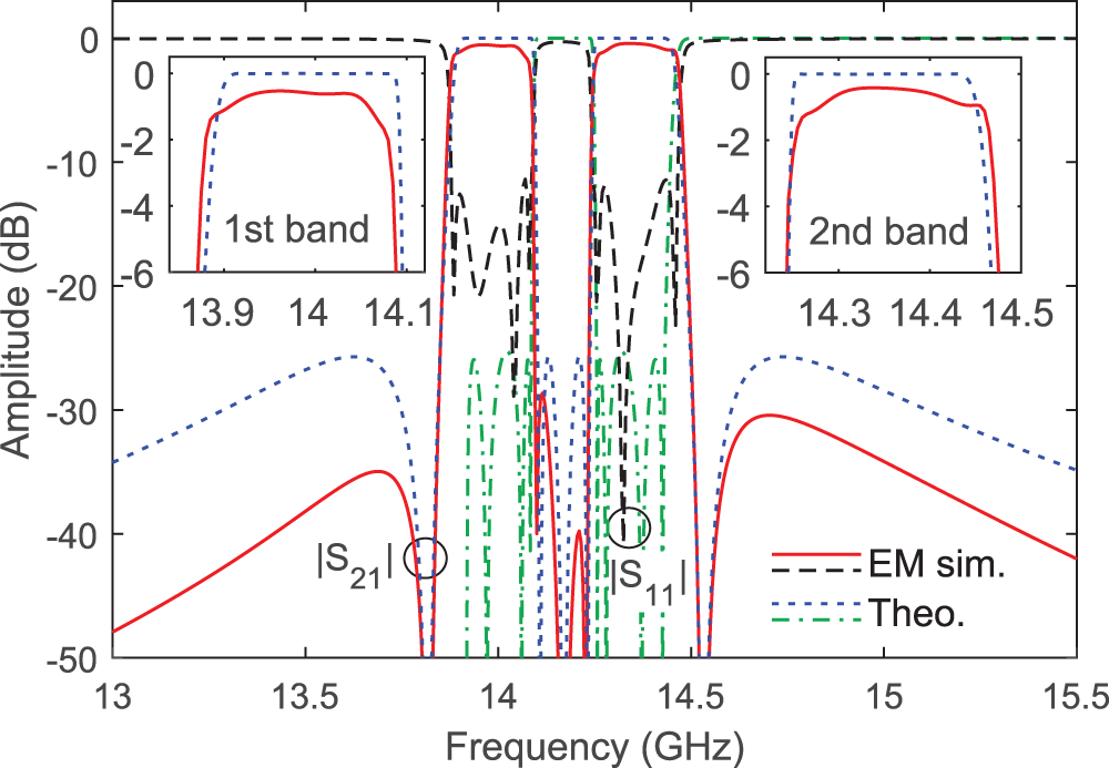
To demonstrate the experimental viability of the proposed approach of GGW sharp-rejection multi-band BPF based on input $/$output multi-extracted cavities and the split-type single-to-multi-band frequency transformation, a proof-of-concept prototype of Ku-band fourth-order dual-band BPF has been EM simulated, manufactured, and characterized. Its theoretical design starts from the normalized coupling-routing diagram introduced in the Coupling-routing diagram and design examples section – see the bottom part of Figure 1 – for the conceived high-selectivity dual-passband filter, while its physical realization relies on the GGW structure designed in the Core GGW section – see Figure 4 – serving as the core transmission medium. The prefixed specifications for the lower and upper passbands are as follows: center frequencies approximately equal to 14 and 14.4 GHz, respectively, and identical 3-dB absolute bandwidths of 200 MHz for both transmission bands – which correspond to 3-dB fractional bandwidths of 1.44% and 1.3%, respectively. The top/bottom, lateral, and 3-D views of the geometrical layout of the developed Ku-band multi-extracted-cavity fourth-order dual-band BPF circuit are depicted in Figure 5. As shown, a symmetrical configuration was adopted, in which the two halves of the structure are implemented on different layers in a vertically stacked arrangement to enhance circuit compactness.
Geometrical layout and associated normalized coupling-routing diagram of the designed prototype of Ku-band multi-extracted-cavity fourth-order dual-band BPF in GGW technology; non-redundant physical dimensions in mm are indicated ( $a_{p}$ and $p$ are the variables designated in Figure 4, $w_{1} = 15.79$ mm, $w_{2} = 8.95$ mm,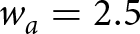 $w_{a} = 2.5$ mm,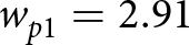 $w_{p1} = 2.91$ mm,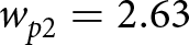 $w_{p2} = 2.63$ mm,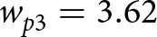 $w_{p3} = 3.62$ mm,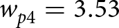 $w_{p4} = 3.53$ mm,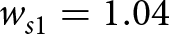 $w_{s1} = 1.04$ mm, $w_{s2} = 2.75$ mm, $w_{s3} = 3.75$ mm,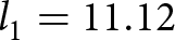 $l_{1} = 11.12$ mm,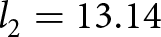 $l_{2} = 13.14$ mm,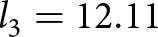 $l_{3} = 12.11$ mm,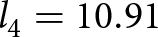 $l_{4} = 10.91$ mm,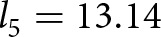 $l_{5} = 13.14$ mm,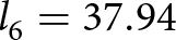 $l_{6} = 37.94$ mm,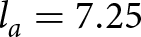 $l_{a} = 7.25$ mm,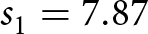 $s_{1} = 7.87$ mm,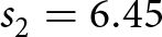 $s_{2} = 6.45$ mm,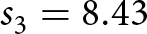 $s_{3} = 8.43$ mm, and all the pins are of the same height [ $h$]). (a) 3-D view of the geometrical layout. (b) Top and bottom views of the geometrical layout – left-hand side – illustrating the cavity numbering and the corresponding couplings as labeled in its associated normalized coupling-routing diagram – right-hand side. (c) Lateral view of the geometrical layout.

Figure 5 Long description
The image consists of three parts illustrating a multi-extracted-cavity fourth-order dual-band bandpass filter in GGW technology. The first part, labeled (a), shows a 3-D view of the geometrical layout. It includes a top lid with resonant-cavity tuning screws, a bottom lid and a WR-62 waveguide-to-coaxial connector. The coupling tuning screw is visible and the structure is marked with P1 and P2 at the ends. The second part, labeled (b), presents the top and bottom views of the geometrical layout on the left, illustrating cavity numbering and couplings. The right side shows the associated normalized coupling-routing diagram with elements like M subscript S4, L, M subscript S1, L and others, along with symbols such as Omega subscript B and Alpha subscript 1. The third part, labeled (c), provides a lateral view of the geometrical layout, showing the top and bottom layers with symmetry indicated. The axes x, y and z are marked and the structure is shown in a vertically stacked arrangement.
EM-simulated and theoretical – i.e., normalized coupling-routing diagram in Figure 5(b) translated to the bandpass domain with the normalized-lowpass-to-bandpass frequency transformation 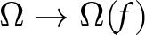 $\Omega \rightarrow \Omega(f)$ in (10) – power transmission $(|S_{21}|)$ and input-reflection $(|S_{11}|)$ responses of the designed Ku-band multi-extracted-cavity fourth-order dual-band BPF in GGW technology ( $M_{S,1}$=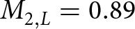 $M_{2,L}=0.89$, $M_{S,3}$ = $M_{S,4}$= $M_{5,L}$ =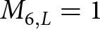 $M_{6,L} = 1$,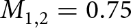 $M_{1,2} = 0.75$,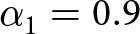 $\alpha_1=0.9$, $\Omega_0$ = $\Omega_A$ =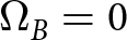 $\Omega_B = 0$, and $\Omega_1=-\Omega_2 = \Omega_3=-\Omega_4 = -1.79$).

Figure 6 Long description
Amplitude (dB) A scientific line plot of S-parameter magnitudes labeled |S21| and |S11| versus frequency. The x-axis label is Frequency (GHz), with labeled ticks at 13, 13.5, 14, 14.5, 15 and 15.5. The y-axis label is Amplitude (dB), ranging from 0 to minus 50 with labeled ticks at 0, minus 10, minus 20, minus 30, minus 40 and minus 50. Legend text shows “EM sim.” and “Theo.” with multiple line styles: a red solid line, a black dashed line labeled EM sim., a blue dotted line and a green dash-dot line labeled Theo. Two inset plots are labeled “1st band” and “2nd band.” Inset labeled “1st band” shows a zoomed frequency span with x-axis tick labels 13.9, 14 and 14.1 and y-axis tick labels 0, minus 2, minus 4 and minus 6. A red solid curve and a blue dotted curve form a near-flat region close to 0, then drop steeply toward minus 6 at both ends of the inset span. Inset labeled “2nd band” shows a zoomed frequency span with x-axis tick labels 14.3, 14.4 and 14.5 and y-axis tick labels 0, minus 2, minus 4 and minus 6. A red solid curve and a blue dotted curve form a near-flat region close to 0, then drop steeply toward minus 6 at both ends of the inset span. In the main plot, the red solid curve is near minus 48 at 13, rises to about minus 35 near 13.7, then drops sharply to near minus 50 just before 14. It rises to near 0 around the first passband region, drops again to near minus 50 around the middle notch region near 14.1 to 14.2, rises again to near 0 around the second passband region and then drops sharply to near minus 50 near 14.5. After 14.5, it rises to about minus 30 near 14.7 and then slopes downward toward about minus 42 by 15.5. A black dashed curve stays near 0 across much of the plot, with several narrow downward dips between about 13.9 and 14.5. A blue dotted curve shows two flat-topped regions near 0 aligned with the two passbands and a broader lower-amplitude shape outside the passbands around minus 25 to minus 35. A green dash-dot curve shows multiple narrow oscillating features between about 14.0 and 14.5, with repeated deep dips approaching minus 50. Text labels “|S21|” and “|S11|” appear inside the plot area.
EM-simulation-based sensitivity analyses of the designed Ku-band multi-extracted-cavity fourth-order dual-band BPF in GGW technology (dimensions in mm). (a) Variation of the lenght  $l_{a}$ of the coupling aperture: step of 0.05 mm. (b) Variation of the width $w_{a}$ of the coupling aperture: step of 0.05 mm. (c) Variation of the window width $s_{1}$ of the inductive-type coupling in the top and bottom layer: step of 0.05 mm. (d) Variation of the window width $s_{2}$ of the inductive-type coupling in the top and bottom layer: step of 0.2 mm.

Figure 7 Long description
The image A showing a line graph with two plotted responses labeled vertical bar S subscript 11 vertical bar and vertical bar S subscript 21 vertical bar. The x-axis is labeled Frequency (gigahertz), ranging from 13 to 15.5 with labeled ticks at 13, 13.5, 14, 14.5, 15 and 15.5. The y-axis is labeled Amplitude (decibel), ranging from 0 to minus 70 with labeled ticks at 0, minus 10, minus 20, minus 30, minus 40, minus 50, minus 60 and minus 70. A legend lists five curves: l subscript a equals 7.15, l subscript a equals 7.2, l subscript a equals 7.25, l subscript a equals 7.3 and l subscript a equals 7.35. The curves show multiple narrow dips between about 14 and 14.6 gigahertz, with several dips reaching near minus 70 decibel. The vertical bar S subscript 21 vertical bar traces form a broad hump around 15 gigahertz near minus 30 decibel and then slope downward toward about minus 40 decibel by 15.5 gigahertz. An arrow annotation near the left side is labeled l subscript a. The image B showing a line graph with responses labeled vertical bar S subscript 11 vertical bar and vertical bar S subscript 21 vertical bar. The x-axis is labeled Frequency (gigahertz), ranging from 13 to 15.5 with labeled ticks at 13, 13.5, 14, 14.5, 15 and 15.5. The y-axis is labeled Amplitude (decibel), ranging from 0 to minus 70 with labeled ticks at 0, minus 10, minus 20, minus 30, minus 40, minus 50, minus 60 and minus 70. A legend lists five curves: w subscript a equals 2.27, w subscript a equals 2.32, w subscript a equals 2.37, w subscript a equals 2.42 and w subscript a equals 2.47. The curves show multiple narrow dips between about 14 and 14.6 gigahertz, with several dips reaching near minus 70 decibel. The vertical bar S subscript 21 vertical bar traces show a broad feature near 15 gigahertz around minus 30 decibel and then decrease toward about minus 40 decibel by 15.5 gigahertz. An arrow annotation near the left side is labeled w subscript a. The image C showing a line graph with responses labeled vertical bar S subscript 11 vertical bar and vertical bar S subscript 21 vertical bar. The x-axis is labeled Frequency (gigahertz), ranging from 13 to 15.5 with labeled ticks at 13, 13.5, 14, 14.5, 15 and 15.5. The y-axis is labeled Amplitude (decibel), ranging from 0 to minus 70 with labeled ticks at 0, minus 10, minus 20, minus 30, minus 40, minus 50, minus 60 and minus 70. A legend lists five curves: s subscript 1 equals 7.79, s subscript 1 equals 7.84, s subscript 1 equals 7.87, s subscript 1 equals 7.94 and s subscript 1 equals 7.99. The curves show multiple narrow dips between about 14 and 14.6 gigahertz, with several dips reaching near minus 70 decibel. The vertical bar S subscript 21 vertical bar traces show a broad feature near 15 gigahertz around minus 30 decibel and then decrease toward about minus 40 decibel by 15.5 gigahertz. An arrow annotation near the left side is labeled s subscript 1. The image D showing a line graph with responses labeled vertical bar S subscript 11 vertical bar and vertical bar S subscript 21 vertical bar. The x-axis is labeled Frequency (gigahertz), ranging from 13 to 15.5 with labeled ticks at 13, 13.5, 14, 14.5, 15 and 15.5. The y-axis is labeled Amplitude (decibel), ranging from 0 to minus 70 with labeled ticks at 0, minus 10, minus 20, minus 30, minus 40, minus 50, minus 60 and minus 70. A legend lists five curves: s subscript 2 equals 6.89, s subscript 2 equals 6.69, s subscript 2 equals 6.45, s subscript 2 equals 6.29 and s subscript 2 equals 6.09. The curves show multiple narrow dips concentrated between about 13.9 and 14.7 gigahertz, with several dips reaching near minus 70 decibel. The vertical bar S subscript 21 vertical bar traces show a broad feature near 15 gigahertz around minus 30 decibel and then decrease toward about minus 40 decibel by 15.5 gigahertz. An arrow annotation near the left side is labeled s subscript 2.
For the implementation of the resonating nodes, GGW rectangular cavities operating in their fundamental TE $_{101}$ resonance mode were employed. The inter-resonator couplings were realized by means of inductive-type irises. The two adjacent GGW cavities interacting across layers – namely, those associated to resonating nodes 1 and 2 in the corresponding normalized coupling-routing diagram of Figure 5(b) – were coupled through an aperture or coupling window etched in the intermediate metallic plane. As a result, an all-inductive-coupling dual-band BPF configuration was obtained, in which finite-frequency out-of-band TZs are generated on both sides of the passbands without requiring capacitive-type couplings. Due to geometrical constraints, the two dangling GGW cavities adjacent to the input and output feeding sections were placed at different positions on opposite sides of the structure. The WR-62-to-coaxial input and output transitions were co-integrated into a single metallic block, as illustrated in Figure 5(a) and (c). Two different types of top and bottom lids were fabricated: one without tuning elements and another incorporating tuning screws located both inside the cavity resonators and within the inductive coupling regions, as shown in Figure 5(a). These tuning elements were included to compensate for fabrication and assembly tolerances that may degrade the measured RF performance of the manufactured GGW dual-band BPF prototype with respect to the EM simulations for the final values of the geometrical design parameters. This choice is justified by the sensitivity analysis presented later in this section as supporting study.
The EM-simulated power-transmission and input-reflection responses of the designed Ku-band GGW dual-band BPF, together with the theoretical responses obtained from the associated coupling-routing diagram shown in Figure 5(b) – i.e., particular case of the  $N$th-order dual-band coupling-routing diagram at the bottom of Figure 1 for $N=4$ – are plotted in Figure 6. The EM simulations were performed with the commercial EM software Ansys HFSS. For comparison purposes, the theoretical responses were translated from the normalized lowpass domain by applying the following frequency transformation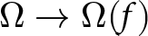 $\Omega \rightarrow \Omega(f)$:
 \begin{equation}
\Omega \rightarrow \Omega(f)=\left(\frac{f_d}{b}\right)\left(\frac{f}{f_d}-\frac{f_d}{f}\right)
\end{equation}
\begin{equation}
\Omega \rightarrow \Omega(f)=\left(\frac{f_d}{b}\right)\left(\frac{f}{f_d}-\frac{f_d}{f}\right)
\end{equation}with 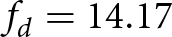 $f_d=14.17$ GHz and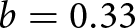 $b=0.33$ GHz as inter-band frequency and scaling-factor parameters, respectively. These theoretical responses were matched to the EM-simulated results through an optimization procedure carried out using Matlab $^{\text{TM}}$. As observed, two sharp-rejection transmission bands are achieved at the target center-frequency positions, together with the five expected finite-frequency out-of-band TZs distributed at both sides of the passbands, three of which are located between the two transmission bands.
Photographs – different views – of the manufactured prototype of Ku-band multi-extracted-cavity fourth-order dual-band BPF in GGW technology (overall dimensions without the input $/$output connector block: $99.42 \times 59.31 \times 25.34$ mm $^{3}$). (a) Internal view. (b) View with top $/$bottom lids without tuning screws. (c) View with top $/$bottom lids with tuning screws.

Figure 8 Long description
Three photographs labeled left parenthesis a right parenthesis comma left parenthesis b right parenthesis comma and left parenthesis c right parenthesis show the same machined metal assembly on a plain background. Left parenthesis a right parenthesis shows a top angled view of a rectangular base with many parallel fins. A raised rectangular block with two fasteners is mounted near one end. A smaller block protrudes from the side. Left parenthesis b right parenthesis shows an angled view of the assembly with a flat cover plate attached by four corner fasteners. A connector block extends from one side. Left parenthesis c right parenthesis shows another angled view of the covered assembly. Multiple fasteners are visible on the cover plate and the connector block extends from one side.
EM-simulated and measured power transmission  $(|S_{21}|)$, input-reflection $(|S_{11}|)$, and in-band group-delay $(\tau_{g}^{21})$ responses of the manufactured prototype of $Ku$-band multi-extracted-cavity fourth-order dual-band BPF in GGW technology. (a) Measurements realized using top $/$bottom lids without tuning screws: $|S_{21}|$ and $|S_{11}|$. (b) Measurements in (a) represented in a broader frequency range. (c) Measurements realized using top $/$bottom lids with tuning screws after adjustment of screws: $|S_{21}|$ and $|S_{11}|$. (d) Measurements realized using top $/$bottom lids with tuning screws after adjustment of screws: $\tau_{g}^{21}$ for lower – i.e., 1st band – and upper – i.e., 2nd band – passbands.

Figure 9 Long description
The image A showing a line graph with y-axis label Amplitude (decibel) and x-axis label Frequency (gigahertz). The x-axis ranges from 13 to 15.5. The y-axis ranges from 0 to minus 50. A legend at upper right shows Meas. (without screws) and EM sim. Two labeled traces appear for vertical bars S subscript 2 1 vertical bars and vertical bars S subscript 1 1 vertical bars, with multiple line styles. The vertical bars S subscript 2 1 vertical bars trace forms two flat-topped high regions near 0 between about 13.9 to 14.1 and about 14.3 to 14.5, with sharp drops to near minus 50 around about 13.8, about 14.2 and about 14.55. Outside these regions the vertical bars S subscript 2 1 vertical bars trace stays between about minus 30 and minus 50 from 13 to 13.8 and from about 14.6 to 15.5. The vertical bars S subscript 1 1 vertical bars trace stays near 0 for most frequencies and shows several narrow dips between about 13.9 and 14.5, reaching below minus 10 and down toward about minus 40 at the deepest points. The image B showing a line graph with y-axis label Amplitude (decibel) and x-axis label Frequency (gigahertz). The x-axis ranges from 10 to 20. The y-axis ranges from 0 to minus 70. A legend at upper right shows Meas. A dashed trace labeled vertical bars S subscript 1 1 vertical bars stays near 0 across the full range. A solid trace labeled vertical bars S subscript 2 1 vertical bars varies between about minus 30 and minus 70, with multiple deep notches below minus 60 between about 10 and 13 and a cluster of narrow high regions near 0 around about 14. A text label Spurious peaks appears near the right side around about 17 to 19, where the solid trace shows several narrow peaks and dips. The image C showing a line graph with y-axis label Amplitude (decibel) and x-axis label Frequency (gigahertz). The x-axis ranges from 13 to 15.5. The y-axis ranges from 0 to minus 50. A legend at lower right shows Meas. (with screws). A dashed trace labeled vertical bars S subscript 1 1 vertical bars stays near 0 except for several dips between about 13.9 and 14.5. A solid trace labeled vertical bars S subscript 2 1 vertical bars forms two flat-topped high regions near 0 between about 13.9 to 14.1 and about 14.3 to 14.5, with sharp drops to near minus 50 around about 13.8, about 14.2 and about 14.55. Two inset plots are shown: the left inset is labeled 1st band with x-axis ticks 13.9, 14, 14.1 and y-axis ticks 0, minus 2, minus 4, minus 6; the right inset is labeled 2nd band with x-axis ticks 14.3, 14.4, 14.5 and y-axis ticks 0, minus 2, minus 4, minus 6. In both insets, the solid trace stays close to 0 across the band with small variations. The image D showing two separate line graphs side by side. Both have y-axis label Time (nanosecond) and x-axis label Frequency (gigahertz). The left graph is labeled 1st band and shows x-axis from 13.8 to 14.2 and y-axis from 0 to 15. A legend text reads Meas. (with screws). The plotted curve rises from near 0 to a peak above 10 near about 13.9, then decreases to around 4 to 6 through about 14.0 to 14.15, then rises again to near 15 close to about 14.18 before dropping back toward 0 near 14.2. The right graph is labeled 2nd band and shows x-axis from 14.2 to 14.6 and y-axis from 0 to 15. The curve rises sharply to near 15 just above 14.2, then decreases to around 4 to 6 through about 14.3 to 14.45, then rises again to above 10 near about 14.5 before dropping toward 0 near 14.6. Both graphs include a label tau subscript g superscript 2 1 near the mid to upper part of the curves.
To further evaluate robustness against fabrication tolerances, EM-simulation-based sensitivity analyses were conducted for the designed GGW  $Ku$-band multi-extracted-cavity fourth-order dual-band BPF shown in Figure 5. Figure 7 illustrates the impact on its EM-simulated power transmission and input-reflection responses caused by variations in several representative physical dimensions of its structure. Specifically, perturbations of the following geometrical parameters were considered in this study – the considered variations were chosen to match or exceed tolerances of the manufacturing process employed for the RF prototype of this work: (i) the aperture length $l_{a}$ (Figure 7(a)), (ii) the aperture width $w_{a}$ (Figure 7(b)), (iii) the window width $s_{1}$ of the inductive-type coupling in the top and bottom layers (Figure 7(c)), and (iv) the window width $s_{2}$ of the inductive-type coupling in the top and bottom layers (Figure 7(d)). As observed, depending on which parameter is being altered, even small variations in these dimensions produce perceptible modifications in the frequency responses of the GGW dual-band BPF prototype. These effects manifest in changes in the in-band input-power-matching levels, bandwidths, out-of-band rejection profile, and $/$or the location of the TZs, as well as the frequency spacing between the two passbands. In particular, the inter-band spacing either increases or decreases depending on the effective coupling strength between pairs of cavities derived from the split-type dual-band frequency transformation, which is mainly controlled by the window width $s_{2}$. These observations highlight the importance of a precise fabrication and justify the inclusion of tuning screws to mitigate $/$compensate such undesired manufacturing imperfections in practical implementations.
A photograph of the developed prototype of GGW  $Ku$-band multi-extracted-cavity fourth-order dual-band BPF is shown in Figure 8. The structure was manufactured using a computer numerical control (CNC) milling machine with a mechanical precision of 0.02 mm, employing aluminum 6061 alloy with a conductive oxidation surface treatment. The measured power transmission, input-reflection, and in-band group-delay responses – obtained using both types of lids, i.e., without and with tuning screws – of this prototype are compared with the EM-simulated results in Figure 9. The measurements were performed using a Keysight 5224A vector network analyzer. As illustrated in Figure 9(a), a reasonable overall agreement between simulations and measurements is observed for the untuned case except for a degradation in the in-band input-power-matching levels, which is attributed to fabrication and assembly tolerances – as revealed by the sensitivity analysis shown in Figure 7. These discrepancies are effectively corrected through tuning, as confirmed by the results in Figure 9(c) and (d). After tuning, the main measured characteristics of the fabricated GGW dual-band BPF are as follows. For the lower and upper passbands, the center frequencies are 14.04 and 14.43 GHz, respectively, with 3-dB absolute bandwidths of 211 and 209 MHz – corresponding to 3-dB fractional bandwidths of 1.5 $\%$ and 1.45 $\%$. The minimum in-band power-insertion-loss levels are 0.9 and 0.76 dB, while the in-band return-loss levels exceed 15.1 and 15 dB, respectively. The maximum in-band group-delay variations are 7.7 ns for the lower band and 10.3 ns for the upper band. Finally, the measured finite-frequency TZs are located at 13.86, 14.17, 14.24, 14.3, and 14.6 GHz, confirming the sharp-rejection characteristics of the proposed filter design. Finally, note that narrow-band spurious spikes attributed to higher-order modes can be observed in Figure 9(b) within the frequency range 18–20 GHz of the measured 10–20-GHz interval. The partial $/$total mitigation of these undesired transmission peaks or their displacement to higher frequencies using different well-known design strategies from classic rectangular-waveguide filters – e.g., mode-selective coupling, cavity-shape optimization including ridged- or stepped-cavity geometries, or undesired-mode absorption by means of deliberately embedded RF lossy elements – remains as further research work.
Comparison with the state-of-the-art
A comparison with the most relevant prior-art works in the field of GGW RF filtering components is summarized in Table 1. The values therein contained have been estimated as best as possible from measured or EM-simulated data when not directly provided. Most of these implementations correspond to single-band BPFs or to combinations of two BPFs forming diplexers, highlighting the scarcity of multi-band BPF devices based on GGW technology.
Comparison with prior-art RF single- and dual-band BPFs and RF diplexers in GGW technology

Table 1 Long description
The table compares groove gap waveguide RF prototypes (single-band bandpass filters, dual-band bandpass filters, and diplexers) by filter order, center frequency, fractional bandwidth, insertion loss, in-band input matching, presence/count of transmission zeros, and circuit size when available. Single-band filters cover a wide frequency range (about 13.97 to 145 GHz) with fractional bandwidths from roughly 0.9% to 18.3%; reported insertion losses are commonly around ≥0.38 to ≥2.21 dB, with the lowest listed value ≥0.22 dB at 32.8 GHz. Input matching values are generally at least 9 to 21 dB across entries. Transmission zeros are inconsistently reported: several single-band designs list none, while others list between 1 and 6; the highest single-band count shown is 6 at 15.12 GHz. Diplexers list paired channel metrics (e.g., 59.5/62.5 GHz and 14.45/15.11 GHz) with insertion losses around ≥0.51 to ≥1 dB; transmission zeros are reported for some diplexers but not all. Dual-band filters list two center frequencies per design (about 13.67/16 to 27.8/36 GHz) with insertion losses typically ≥0.38 to ≥0.9 dB and transmission-zero counts from 3 to 8; the “this work” dual-band entry is order 4 at 14/14.4 GHz with ≥0.9/0.76 dB loss, ≥15.1/15 dB matching, 5 transmission zeros, and a stated size of 99.42×59.31×25.34 mm (also given as 4.64×2.77×1.18 in normalized wavelength units). Size data are missing for many references, and some orders, losses, matching, and transmission-zero counts are marked as estimated or limited to what was visible in figures, so cross-paper comparisons may be incomplete.
BPF = bandpass filter; FBW = fractional bandwidth; GGW = groove gap waveguide; TZ = transmission zero; N.A. = not applicable or available; T.W. = this work;  $^{\dagger}$ = estimated from graphs or data from simulations;
# = For TZs, only those observed in the corresponding figure are reported, although additional TZs may exist outside the shown frequency range; for the circuit size, the values are taken directly from the corresponding reference;  $^{\ast}$ = performance metrics for differential-mode operation; $\lambda_0$ = wavelength at vacuum at the center frequency for single-band BPFs, at the center frequency of the lower passband for dual-band BPFs, and at the center frequency of the lower channel for diplexers.
From Table 1, it can be concluded that the  $Ku$-band GGW dual-band BPF prototype of this work exhibits competitive RF performance compared with the previously reported GGW dual-band BPFs in [Reference Malki, Yang and Gómez-García29, Reference Huang, Zhang, Zhou, Lu, Tam, Zhang and Tang43–Reference Malki, Yang and Gómez-García45]. Specifically, the GGW dual-passband filters in [Reference Huang, Zhang, Zhou, Lu, Tam, Zhang and Tang43] and [Reference Wu, Wu, Yao, Huang, Xu and Wang44] are restricted to second-order experimental validations and rely on more sensitive cross-coupling schemes for TZ generation. In addition, they feature fewer finite-frequency stopband TZs than the proposed filter. The dual-band BPFs reported in [Reference Malki, Yang and Gómez-García29], in both reflective and reflectionless configurations, are based on quadruplet networks to achieve quasi-elliptic-type dual-passband responses. Consequently, their physical implementations require both inductive- and capacitive-type couplings, increasing structural complexity. In contrast, the GGW dual-band BPF in [Reference Malki, Yang and Gómez-García45] employs a reactive load or oversized GGW cavity connected at the input port of a low-selectivity GGW dual-band BPF unit to produce multiple out-of-band TZs without cross coupling. However, the overall transfer-function envelope is still governed by the low-order dual-band BPF unit, resulting in reduced attenuation levels in some out-of-band regions but in-band low-loss characteristics as main advantage. Furthermore, the lower and upper cut-off slopes of the first and second passbands – measured from the 3-dB cut-off frequency to the nearest 40-dB stopband frequency relative to the minimum insertion-loss level – are 207.2 and 93.9 dB $/$GHz for the filter in [Reference Malki, Yang and Gómez-García45], respectively. These values are significantly lower than those achieved by the developed GGW $Ku$-band multi-extracted-cavity dual-band BPF prototype, which are equal to 787.2 and 743 dB $/$GHz for the referred cut-off slopes, respectively.
Finally, it is worth noting that the experimental validation of the proposed GGW sharp-rejection multi-band BPF concept for implementations with more than two passbands, or operating above the Ku-band, can be readily achieved by incorporating additional inductively coupled cavities or by using higher-precision fabrication processes. Consequently, these extensions do not introduce any fundamental or additional technological challenges beyond those already encountered in the present GGW filter prototype.
Conclusion
A new class of  $Ku$-band GGW sharp-rejection multi-band BPFs based on a multi-extracted-cavity configuration has been reported. The engineered solution is derived from a GGW single-band BPF comprising one-pole $/$two-TZ input and output feeding networks, which is subsequently transformed into a multi-band BPF by means of a split-type single-to-multi-band frequency mapping. The resulting coupling-routing topology has been detailed and theoretically validated through both frequency-symmetrical and asymmetrical design examples, each incorporating multiple stopband TZs. These synthesis examples highlight the strong versatility of the approach with respect to independent control of the center frequencies and bandwidths for the passbands, as well as precise positioning of the out-of-band TZs. In addition, a sensitivity study of the most influential physical parameters has been carried out, offering valuable design guidance and justifying the inclusion of tuning screws to compensate for fabrication inaccuracies. To experimentally verify the concept, a compact two-layer vertically stacked GGW fourth-order dual-band BPF has been fabricated and characterized, exhibiting five out-of-band TZs and passbands centered at 14 and 14.4 GHz. The measured results are in close agreement with the full-wave EM simulations, confirming the high selectivity, sharp rejection, compact form factor, and practical viability of the proposed filter approach. Overall, the presented topology and synthesis methodology provide a robust and scalable framework for the development of GGW highly selective multi-band BPFs targeting advanced $Ku$-band-and-beyond RF-wireless communications and sensing applications.
Funding statement
This work has been supported by the Spanish Ministry of Economy, Industry, and Competitiveness (State Research Agency) under Project PID2023-149096OB-I00.
Competing interests
The author(s) declare none.

Mohamed Malki received the B.Sc. degree in Telecommunication Engineering, the M.Sc. degree in Telecommunication Engineering in the specialized area of Space and Defense Technologies, and the Ph.D. degree in Electrical Engineering (with honors) from the University of Alcalá, Madrid, Spain, in 2020, 2022, and 2024, respectively. In 2022, he joined the Department of Signal Theory and Communications at the University of Alcalá, Madrid, Spain, as a Research Assistant. He was a Visiting Researcher with the Emerging Device Technology (EDT) Research Lab at the University of Birmingham, U.K., in 2023. His main research interests include the analysis, design, and implementation of microwave filters and multiplexers. He has authored/co-authored 27 papers in international journals and conferences. In addition, he has served as an IEEE MTT-S Student Ambassador since 2024. Dr. Malki was the recipient of the 2023 HISPASAT Award for the Best M.Sc. Thesis in New Technologies for Communication Satellites and the 2024 HISPASAT Award for the Best Ph.D. Thesis in Satellite Communication Systems from the Official College of Telecommunication Engineers and the Spanish Association of Telecommunication Engineers (COIT/AEIT), the 2023 European Microwave Association (EuMA) Internship Award, and the First Best Paper Award at the 2024 IEEE International Microwave and Antennas Symposium (IMAS).

Roberto Gómez García received the Telecommunication Engineer and Ph.D. degrees from the Polytechnic University of Madrid, Madrid, Spain, in 2001 and 2006, respectively. He is currently a Full Professor at the Department of Signal Theory and Communications, University of Alcalá, Alcalá de Henares, Spain. His current research interests include the design of fixed $/$tunable high-frequency filters and multiplexers in planar, hybrid, and monolithic microwave-integrated circuit technologies, multifunction circuits and systems, software-defined radio and radar architectures for telecommunications, remote sensing, and biomedical applications, and displacement RF sensors. In these topics, he has authored $/$co-authored about 170 articles in international journals and 200 articles in international conferences. Dr. Gómez-García serves as a member for the Technical Review Board for several IEEE and EuMA conferences. He is also a member of the IEEE MTT-S Filters (MTT-5), the IEEE MTT-S RF MEMS and Microwave Acoustics (MTT-6), the IEEE MTT-S Wireless Communications (MTT-23), and the IEEE MTT-S Biological Effects and Medical Applications of RF and Microwave (MTT-28) Technical Committees, and was member of the IEEE CAS-S Analog Signal Processing Technical Committee. He was a recipient of the 2016 IEEE Microwave Theory and Techniques Society (MTT-S) Outstanding Young Engineer Award. He was an IEEE CAS-S Distinguished Lecturer (2020–2022). He was an Associate Editor of IEEE Transactions on Microwave Theory and Techniques from 2012 to 2016, IEEE Transactions on Circuits and Systems-I: Regular Papers from 2012 to 2015, IEEE Microwave and Wireless Components Letters from 2018 to 2020, as well as other journals such as IEEE Access, IET Microwaves, Antennas, and Propagation, and the International Journal of Microwave and Wireless Technologies, and the IEEE Journal OF Electromagnetics, RF and Microwaves in Medicine and Biology. He was a Senior Editor of the IEEE Journal on Emerging and Selected Topics in Circuits and systems from 2016 to 2017 and the MTT-S Newsletter Working Group Chair from 2019 to 2021. He was a Guest Editor for several special $/$Focus issues and sections in IEEE and IET journals. He was the Editor-in-Chief of the IEEE Microwave and Wireless Technology Letters (2022–2024). Currently, he is a TC-5 Topic Editor of the IEEE Journal of Microwaves, a Senior Editor of IEEE Transactions on Circuits and Systems-I: Regular Papers, and a Track editor of Electromagnetic Science. He is now an elected member of the MTT-S Administrative Committee. He was the co-recipient of the Best Paper Award at the IEEE 2024 International Microwave and Antennas Symposium.










 Open access

