


Introduction
Millimeter waves are being used extensively for commercial applications. Recent frequency allocation of the 76–81 GHz band for automotive radar sensor applications [1] has allowed development for such sensors for driver assistance systems. An important component of radar sensors is the antenna. It determines the most important range and field of view properties of the radar sensor. The antenna design is hence a very crucial part of the sensor development.
For many commercially available sensors, single layer printed circuit board (PCB) antennas such as the microstrip (MS) patch antenna or the substrate integrated waveguide antenna are used in antenna arrays. For small substrate thicknesses, these antennas suffer from narrow impedance bandwidth [Reference Menzel and Moebius2]. Due to single sided feeds and linear arrays, such antennas also have relatively narrow radiation pattern bandwidths. Recent multilayer antenna designs employing wideband antenna elements such as the grid array antenna [Reference Bauer and Menzel3–Reference Khan, Meyer, Baur and Waldschmidt5], when used as linear arrays fed in the center, have larger impedance bandwidths as well as larger radiation pattern bandwidths. Such designs rely on multilayer PCB and hence are more expensive and complex to manufacture than single layer PCB designs.
Recently, a hybrid approach to designing multilayer antennas was demonstrated by the authors [Reference Khan, Meyer, Baur and Waldschmidt6]. Instead of employing a multilayer PCB, this approach uses a single layer PCB and multilayer thin films that house the complete antenna element. These thin films are attached at the radiating positions on the PCB. In addition to being simpler to manufacture, this approach is also more flexible in terms of combination of antenna elements and feed network, as was shown in [Reference Khan, Meyer, Baur and Waldschmidt6] where the same antenna element was integrated with three different feed networks.
This work presents a novel multilayer grounded coplanar waveguide (GCPW) fed aperture coupled stacked patch (ACSP) antenna using the explained hybrid approach. The GCPW feed network is realized on the single layer PCB, whereas the stacked aperture coupled patch is realized on a multilayer thin film. This paper is organized as follows: the section “Antenna design” describes the design and attachment process for the antenna. The section “Array design” describes the array design where a compact power divider is described. Measurement results are provided in the section “Measurement results”. In the section “Comparison of multilayer antenna concepts”, a comparison in terms of antenna performance and manufacturing aspects is performed between multilayer PCB antennas and those based on the presented hybrid approach. The paper concludes with the section “Conclusion”.
Antenna design
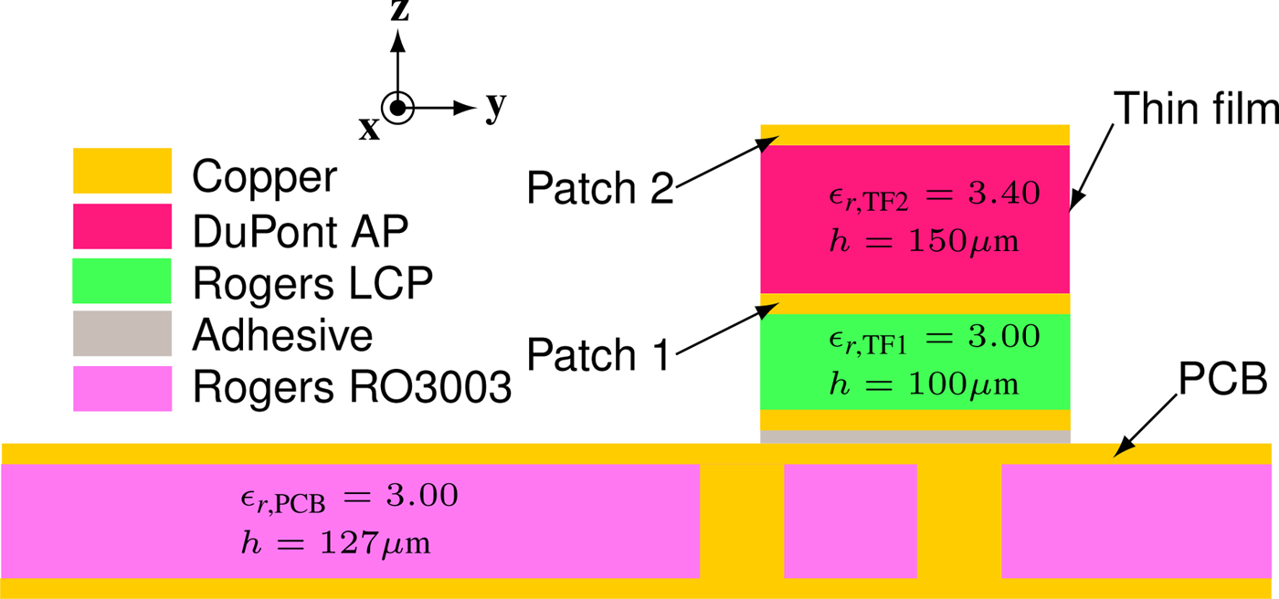
The layer construction of the antenna is shown in Fig. 1 A multilayer low loss RF qualified thin film houses the complete antenna element. It is attached to the single layer PCB using a non-conducting epoxy-based adhesive [7]. The thin film consists of two substrate layers, Rogers Ultralam liquid crystal polymer (LCP) with εr,TF1 = 3.00 and h = 100 μm, and Dupont Pyralux AP and DuPont LF adhesive stackup with ε r,TF2 = 3.40 and h = 150 μm. Hence, the total thin film thickness, excluding metal layer thickness is around 250 μm. The single layer PCB consists of a Rogers RO3003 substrate with ε r,PCB = 3.00 and h = 127 μm.
Layer construction of antenna.
Element design
The radiating element is a stacked rectangular patch structure. Each substrate layer of the thin film has a rectangular patch element etched on it. A transverse slot etched on the top metal layer of the PCB couples the energy to the thin film. The feed network is also etched on the PCB. The different layers of the stacked patch single element are shown in Fig. 2.
Single stacked patch antenna element (a) Patch 1 (b) Patch 2 and (c) PCB top layer.
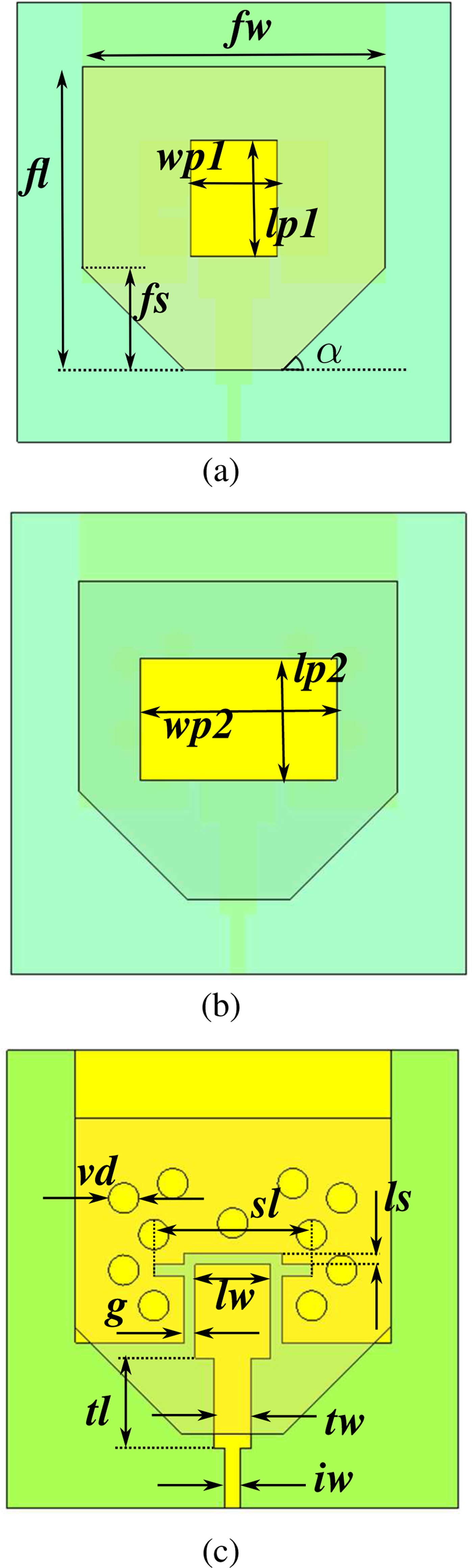
The feed network terminates in a MS to GCPW transition which has the transverse slot at the end of it. The MS line with width iw transforms to a GCPW with transformer length tl and width tw. The GCPW center conductor has a width lw. The center conductor of the GCPW is extended by length ls to improve the impedance match to the slot. The slot at the end of the GCPW has length sl and width g. A similar feeding method based on coplanar waveguide (CPW) was investigated in [Reference Mestdagh and De Raedt8]. The main difference here is the use of a ground plane below the CPW to shield the feed network, as well as the use of fencing vias with diameter vd around the excitation slot to reduce surface waves and hence increase the efficiency of the antenna.
The thin film is placed on the PCB such that the excitation slot is aligned with the center of the patches. An originally rectangular thin film with width fw and length fl is used to house the stacked patches. The thin film is altered by removing triangular portions defined by angle α and length fs in order to minimize the effect of the film on the feed network on the PCB.
The dimensions of the stacked patches are wp1 and lp1 for Patch 1 and wp2 and lp2 for Patch 2, respectively. The length and width of the patch elements, along with that of the excitation slot was optimized to result in two impedance resonances which enable a wideband impedance match. The coupling effect of each resonance was adjusted to achieve maximum impedance bandwidth. The final values of all design parameters are listed in Table 1.
Design parameters for GCPW ACSP antenna
All length dimensions are in mm.
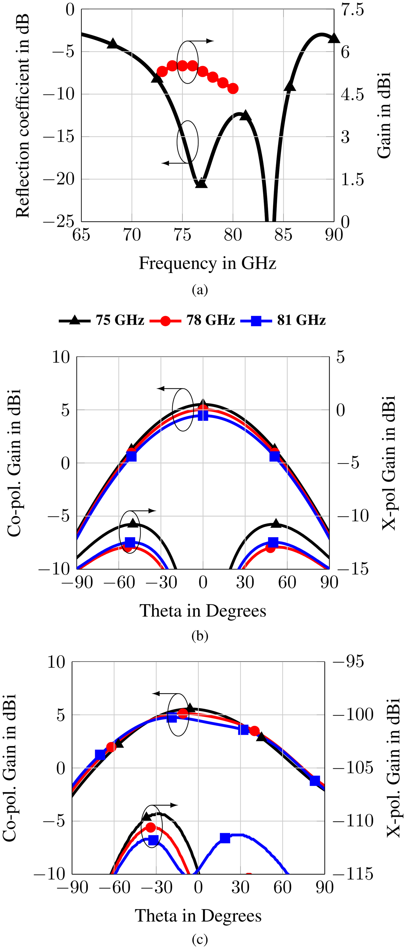
Simulation results for a single stacked patch element are shown in Fig. 3. Reflection coefficient and gain results are shown in Fig. 3(a). In the reflection coefficient result, two resonance dips can be seen, due to the coupled resonances of the stacked patches. A wideband impedance match of 15% (73.4–85.4 GHz) is achieved. The simulated gain of the single element is a maximum of 5.5 dBi at 75 GHz and remains within 1 dB of the maximum from 73 to 85 GHz. Farfield radiation patterns in the H-Plane and E-Plane are shown in Figs 3(b) and 3(c), respectively. Broadisde radiation over the complete frequency range can be seen for the H-Plane results. A beam squint of upto 6° in the negative Theta direction is however observed in the E-Plane over the operating frequency range. This can be attributed to a slightly asymmetric electric field on the radiating edges of the patch due to the asymmetric ground plane on the PCB top layer below the patch. The 3 dB beamwidths for the H- and E-Plane are 85° and 100°, respectively, at 78 GHz. Cross-polar radiation components are also plotted. In the H-Plane broadside direction, they are suppressed by more than 20 dB. Although the cross-polar component increases for Theta values around ±60°, this is not relevant for the intended array design, which will have a small beamwidth in H-Plane. In the E-Plane cross-polar components are suppressed by more than 100 dB. This shows that the antenna has a high-polarization purity for the intended application.
Simulated reflection coefficient and gain results (a), radiation pattern in H-Plane (b), and radiation pattern E-Plane (c) of single stacked patch element.
Element placement and tolerance analysis
As mentioned earlier, the thin film needs to be placed on the PCB such that the excitation slot is aligned to the center of the patches. This requires an accurate thin film placement mechanism. It is achieved using a die-bonder [9]. An epoxy-based non-conductive paste adhesive with a thickness of about 10 μm is first deposited by the integrated dispenser of the die bonder at the position where the thin film will be placed. Additional structures to assist the pick and place head and integrated camera of the die bonder are etched on the bottom substrate layer of the thin film, as well on the top layer of the PCB. A positioning accuracy of ±7 μm in the x- and y-axis can be achieved using this process, which is within the allowed maximum misalignment for optimum antenna operation.
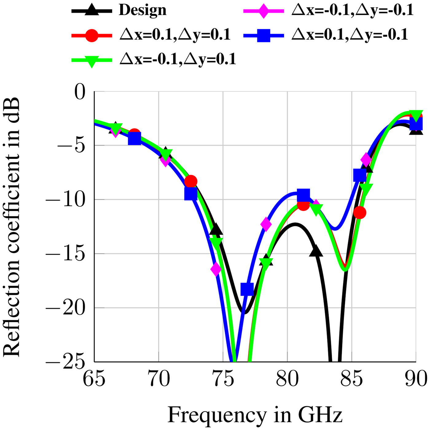
For series production with high volume, standard SMT pick and place machines are used for automotive radar PCB assembly. Depending on the machines used, these errors can range from ±30 upto ±50 μm in the x- and y-axis. The effect of positioning tolerances on the coupling between the PCB and thin film is simulated. Positioning errors of ±0.1 mm are included in the simulations. Reflection coefficient results for these simulations are shown in Fig. 4. It can be seen that the resonance frequencies slightly change and the impedance matching slightly deteriorates, but apart from the Δx = 0.1, Δy = −0.1 case where the reflection coefficient is below −9 dB, all reflection coefficient values stay below −10 dB for the complete operating frequency bandwidth and beyond. Farfield results with positioning errors, not shown here, are virtually the same as for the nominal positioning case. This shows that the thin film antenna design is robust to positioning errors that can occur in series production.
Reflection coefficient single element with thin film positioning errors in mm.
Array design
A 2 × 8 array was designed using the described radiating element. At the design frequency of 77 GHz, the free space wavelength is λ0 = 3.90 mm and the wavelength in the PCB substrate is λg = 2.24 mm. For the E-Plane radiation pattern, the antenna elements were placed in opposite direction. For constructive interference in the broadside direction, a 180° phase difference is required between these two elements. This is conventionally achieved through a λg/2 length extension to one of the feed lines. In the compact design presented, however, such a line extension would result in a large element spacing of about λ0 and hence the introduction of grating lobes in the E-Plane pattern.
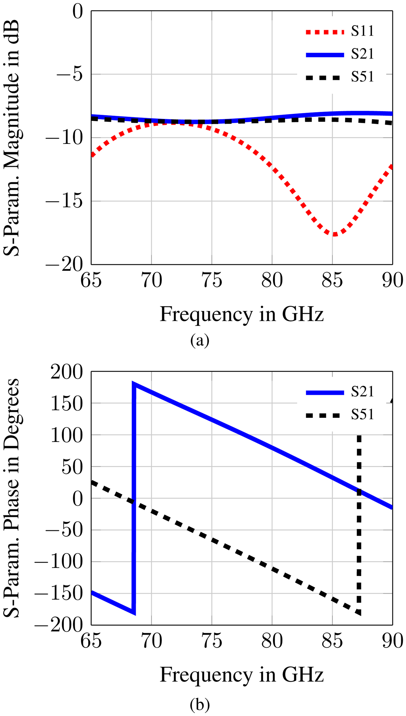
In order to maintain a compact inter-element distance, a novel power divider based on a MS to slotline transition is designed to feed a 2 × 2 sub-array. It is based on the bi-phase divider shown in [Reference Bialkowski and Abbosh10] which was designed for lower frequencies. Essentially, the power divider consists of a MS to slotline transition, followed by a length of slotline, which again transitions back to MS. After the second transition, the opposite phase signals of the slotline couple to the MS lines going in opposite directions to each other and hence the output lines have 180° phase. The designed power divider is shown in Fig. 5. It operates over a wide frequency range. The simulated results of the power divider are shown in Fig. 6. Since it is a symmetrical design, only results for output ports on one side of the power divider are shown. It can be seen that a wideband equal power division is achieved for both output ports, with low reflection coefficient at the input. In addition, a constant 180° phase difference is achieved between the output ports while keeping the power divider compact. By using this power divider, element placement in both E- and H-Planes of de = 2.52 mm (0.65λ0) and dh = 2.60 mm (0.67λ0), respectively, is achieved for the antenna array.
Microstrip-Slotline compact power divider top (a) and bottom (b) view.

S-Parameters magnitude (a) and phase (b) of power divider.
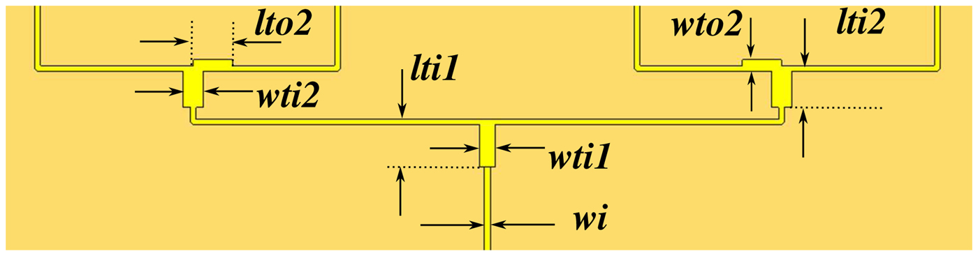
Additionally, a conventional corporate 1 × 4 MS power divider is designed to feed each 2 × 2 sub-array. Consisting of quarter-wave transformers with different output width lines, it does equal power division in the first stage followed by unequal power division in the second stage, providing more power to inner ports. Unequal power division is done to achieve amplitude tapering over the array, thereby reducing side-lobes in the H-Plane. The 1 × 4 power divider design is shown in Fig. 7. The design parameters for both power dividers are listed in Table 2.
Top view of 1 × 4 power divider for array.
Design parameters for power divider

All length dimensions are in mm.
Measurement results
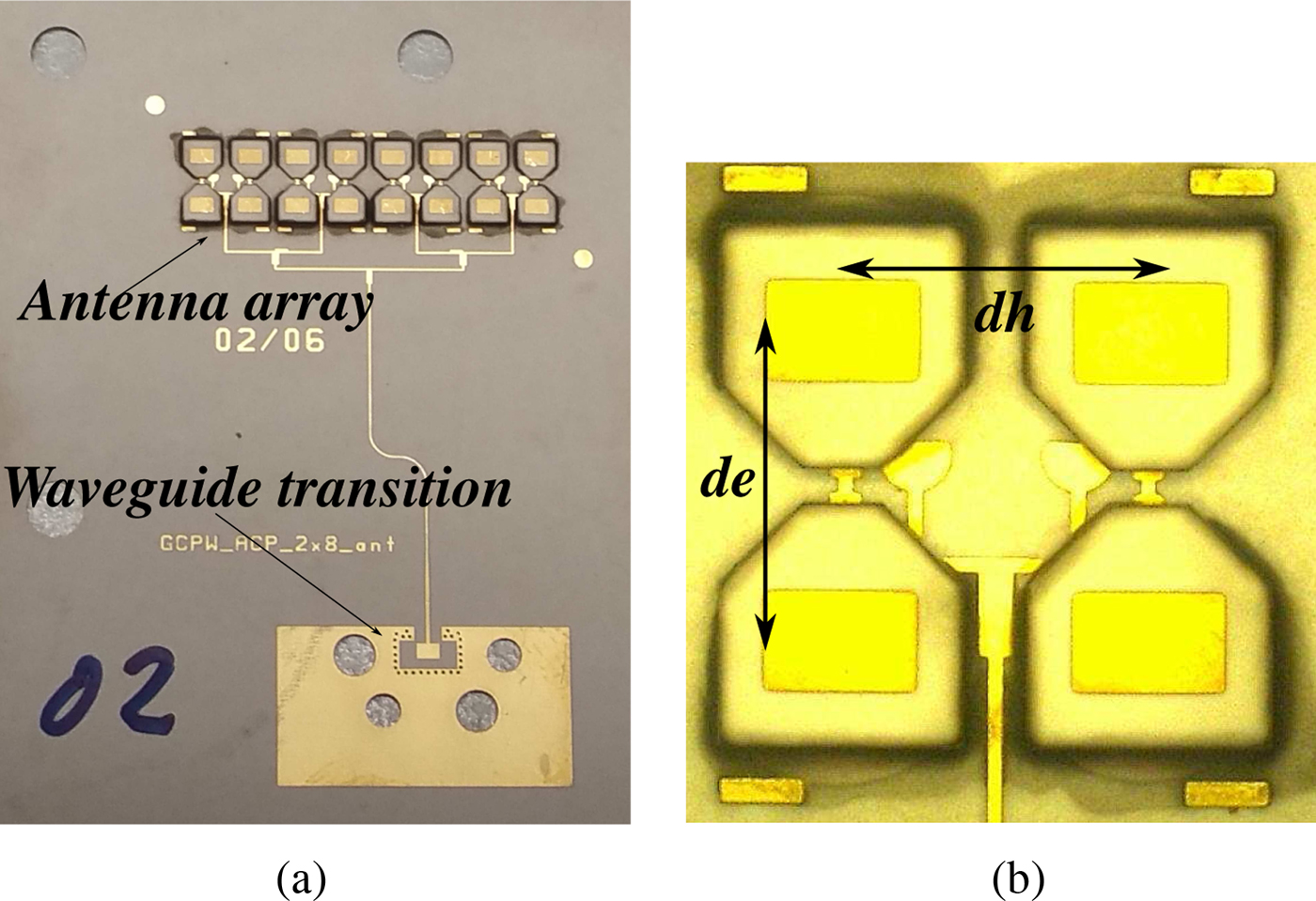
The described 2 × 8 array was manufactured. Two different PCB designs were manufactured. In one design, the array was connected to a GSG-probe transition to enable S-Parameter measurements using a wafer-prober-based setup. In the second design, the array was connected to a MS to waveguide transition to enable antenna pattern measurement. The same waveguide-based measurement setup as used in [Reference Khan, Meyer, Baur and Waldschmidt6] was used for antenna pattern measurement. This manufactured design is shown in Fig. 8. The waveguide transition has been designed and characterized in [Reference Frei11].
Manufactured antenna array for pattern measurement complete (a) view and zoomed in microscope view (b) of 2 × 2 sub-array.
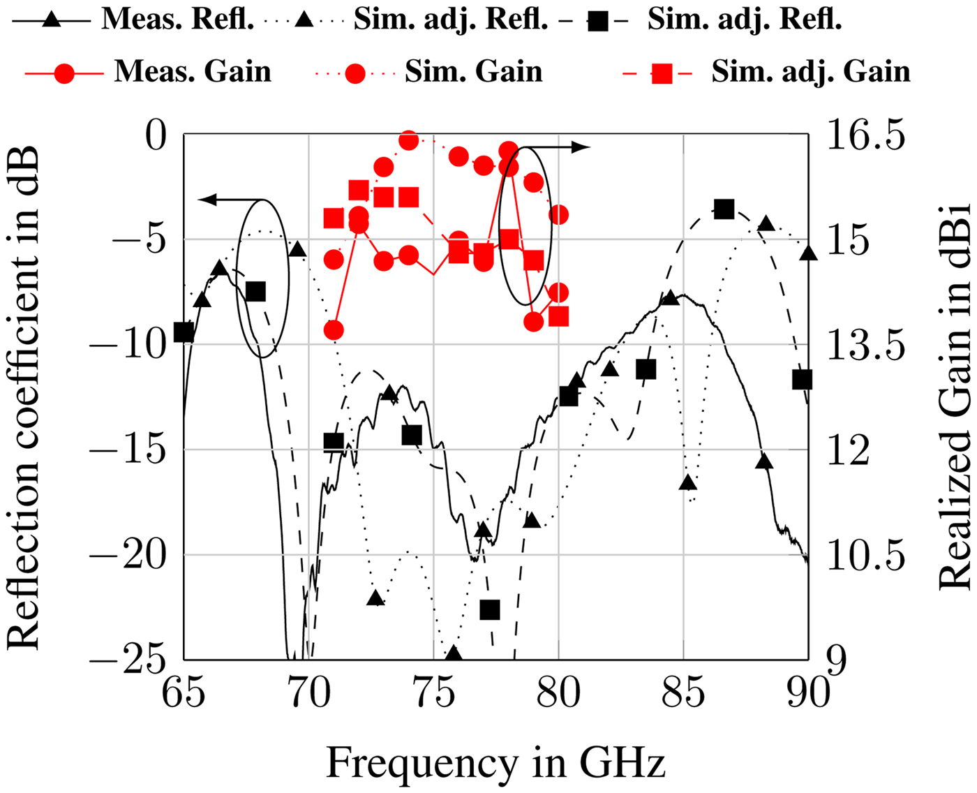
The simulated and measured results for the reflection coefficient and realized gain can be seen in Fig. 9. Also shown are the results of the simulation model during the design process (Sim. Refl. and Sim. Gain), as well as the adjusted simulated results (Sim. adj. Refl. and Sim. adj. Gain) after observing the measured results. It was observed in the measured reflection coefficient results and realized gain results, as well as farfield results (shown in Fig. 10) that the operating frequency of the antenna is approximately 5 GHz lower than the designed operating frequency of 77 GHz. It is known from literature that a shift between simulated and measured frequency performance often results due to a discrepancy in substrate dielectric constant values. As mentioned in the section “Antenna design”, the thin film substrate TF Sub2 consisting of a Dupont Pyralux AP and DuPont LF adhesive stackup was modeled initially as a homogeneous substrate with ε r,TF2 = 3.40. However, the dielectric constant value provided by the manufacturer in the data sheet is only measured up to 20 GHz. Similarly, the epoxy adhesive was modeled initially as an air gap with thickness of 10 GHz, since its dielectric constant value had not been measured at high frequencies [7] either, and it had minimal thickness compared to the other substrate thicknesses.
Simulated and measured reflection coefficient and realized gain results for GCPW ACP antenna array.
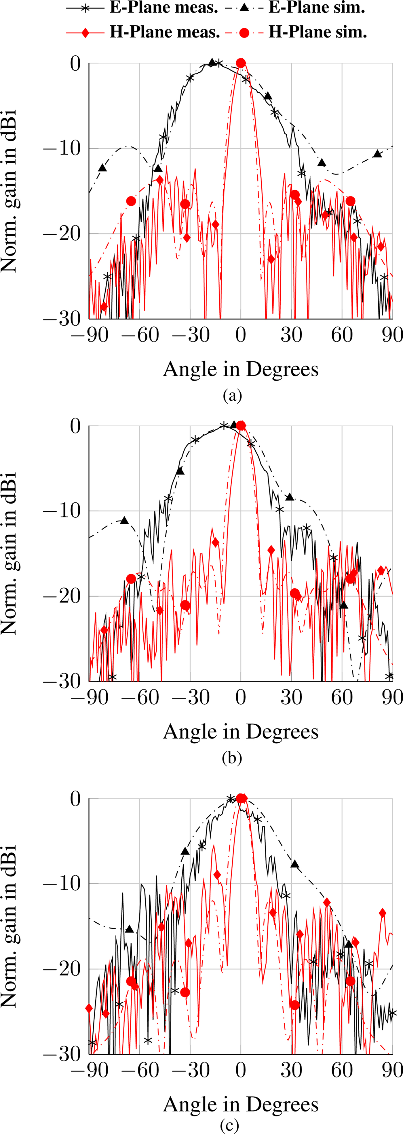
Simulated and measured farfield radiation pattern results at (a) 71 GHz, (b) 73 GHz and (c) 76 GHz in the E-Plane and H-Plane of the 2 × 8 antenna array.
After modeling the thin film substrate TF Sub2 as a homogeneous dielectric with ε r,TF1 = 3.70 and the epoxy adhesive as a homogeneous substrate with ε r,adh = 3.00, the model was simulated again. It can be seen that a better agreement between the measured and simulated reflection coefficient results is achieved with the adjusted simulation model. Two resonance dips, as expected from the single element simulation, can be seen in the measured results. These enable a wideband impedance match. A |S11| < −10 dB impedance matching bandwidth of about 19% (67.9–82.5 GHz) is obtained.
In terms of realized gain, accounting for the losses due to the waveguide transition (0.4 dB) and those of the MS feed line to the antenna (1.5 dB), a maximum measured realized gain of about 15.4 dBi at 72 GHz in the usable frequency region of 71–76 GHz is measured. The realized gain remains within 3 dB of the maximum throughout the measured frequency range of 71–80 GHz.
The measured and simulated farfield radiation patterns are shown in Fig. 10. As explained previously, the operating frequency of the designed antenna is approximately 5 GHz lower than the designed frequency due to dielectric constant modeling errors. Hence, results are shown for 71, 73, and 76 GHz. The substrate modeling correction has been applied to the simulated results. E-Plane and H-Plane co-polarized simulated and measured results are shown. A broadside radiating main lobe is observed in the H-Plane, and a 3 dB beamwidth of 11° is measured. Good side-lobe suppression is observed at 71 and 73 GHz, with a maximum side-lobe level of −12 dB at 73 GHz. The side-lobe reduces to −7 dB at 76 GHz. Lower side-lobes are seen in the simulated results, and the discrepancy is expected to be due to slight tolerances in manufacturing, which can have a large influence on side-lobe suppression. In the E-Plane, there is a squint in the negative direction of about 10° at 71 GHz, which reduces to 3° at 76 GHz. A 3 dB beamwidth of 44° is measured at 71 GHz, which reduces to 36° at 76 GHz. The beam squint and change in E-Plane pattern are due to the asymmetric ground plane below the thin film patch element and is also seen in the simulated results.
Comparison of multilayer antenna concepts
Multilayer antenna concepts for automotive radar have traditionally been based on multilayer PCB designs. In this work, a novel hybrid concept based on single layer PCB and multilayer thin films has been presented. Here, a comparison of both approaches to realize multilayer antennas is presented. As examples, antenna concepts investigated by the authors, as well as other designs reported in the literature are used. For multilayer PCB-based antennas, the designs from the authors include coaxial fed variable width grid array antenna [Reference Khan, Pontes, Li and Waldschmidt4] and SIW slot fed grid array antenna [Reference Khan, Meyer, Baur and Waldschmidt5] As examples of other designs reported in the literature, multilayer grid array antennas reported in [Reference Bauer, Wang and Menzel12] for 79 GHz operation and [Reference Zhang and Zhang13] for 60 GHz operation are used. For the hybrid approach, the aperture coupled stacked patch antenna presented in this work and the stacked grid antenna [Reference Khan, Meyer, Baur and Waldschmidt6] are used as examples. Table 3 summarizes the structural and geometric properties, as well as important performance criteria, for all the antenna designs.
Comparison of multilayer antenna array designs presented

* Thin films with two layers attached additionally at antenna positions
** Additional thickness at thin film position approximately 0.2 mm
Antenna performance
Comparing the multilayer PCB antennas, the designs in [Reference Khan, Pontes, Li and Waldschmidt4,Reference Bauer, Wang and Menzel12,Reference Zhang and Zhang13] achieve a much higher gain, aperture, and radiation efficiency (for the design in [Reference Zhang and Zhang13] no radiation efficiency is reported) than the one in [Reference Khan, Meyer, Baur and Waldschmidt5]. In terms of aperture, all designs use grid array radiating aperture. The difference in performance, with regard to gain, aperture efficiency and radiation efficiency, is explained by the size of, and the losses in, the feed network. In [Reference Khan, Pontes, Li and Waldschmidt4], a short length compact feed network with low loss is realized below the radiating element. It does not cover any area on the radiating layer. Similarly, in [Reference Bauer, Wang and Menzel12,Reference Zhang and Zhang13], the feed network originates on the bottom substrate layer, and multiple substrate layers below the radiating layer are used for it. In [Reference Khan, Meyer, Baur and Waldschmidt5], the feed network originates on the top substrate layer, transfers energy to the second and third substrate layer through SIW structures, before terminating in a slot feed. The length of the feed network is much longer which results in higher losses.
Thin film-based antenna designs realize feed networks on the single layer PCB, with the multilayer antenna implemented on thin films. Considering the array size excluding the feed network, all designs have a similar size. For the designs based on the stacked double grid element, the same radiating aperture is used. As explained in [Reference Khan, Meyer, Baur and Waldschmidt6], the performance difference can be explained by the losses in the feed network. GCPW and MS-based designs have lower loss feed networks compared to the SIW-based one. Hence they achieve higher gain and higher aperture and radiation efficiency. The ACSP antenna presented in this work, however, surpasses the designs in [Reference Khan, Meyer, Baur and Waldschmidt6] for all the mentioned criteria. An important reason for the difference is the compact feed network implemented, including the novel sub-array power divider.
Comparing the best performing multilayer PCB and thin film-based antennas, the ACSP achieves overall performance comparable to the multilayer antennas from [Reference Khan, Pontes, Li and Waldschmidt4,Reference Bauer, Wang and Menzel12,Reference Zhang and Zhang13]. Whereas gain, aperture, and radiation efficiency are slightly higher for the multilayer PCB designs, the impedance matching bandwidth for the ACSP array is higher due to the use of stacked patch radiating elements.
Manufacturing aspects
The multilayer PCB designs vary in terms of a number of substrate layers. In [Reference Khan, Pontes, Li and Waldschmidt4,Reference Zhang and Zhang13], three substrate layers each, in [Reference Bauer, Wang and Menzel12] 12 substrate layers, and in [Reference Khan, Pontes, Li and Waldschmidt4] two substrate layers are used, respectively. In terms of the manufacturing process, multilayer PCB antennas require two or more RF substrates to be stacked on top of each other. Depending on the antenna design used, multilayer layer vias also need to be realized on the PCB. Both of these manufacturing steps can result in manufacturing tolerances, such as layer or via misalignment, in the realized PCB. The number and magnitude of tolerances increase with the number of substrate layers. If manufacturing tolerances occur in a buried layer, they are also much difficult to locate, since they are not optically visible.
For the hybrid thin film antennas, the manufacturing process involves only a single layer RF PCB. The thin films, produced separately only have etched copper structures, do not incorporate vias, and are smaller in size. This makes them simple to manufacture. When attached to the single layer PCB, the feeding method is also based on slots and no galvanic contact is involved. The main source of manufacturing tolerance is the thin film positioning on the PCB. Simulative tolerance analysis was performed for the presented ACSP design in the section “Element placement and tolerance analysis” and the SGA antenna in [Reference Khan, Meyer, Baur and Waldschmidt6]. The results showed that even with thin film positioning errors of ±100 μm simultaneously in both lateral directions, the impedance matching and antenna performance do not get affected significantly. Hence, it can be said that overall manufacturing simplicity and design robustness of hybrid thin film antennas is greater than for multilayer PCB antennas.
Conclusion
A novel multilayer thin film antenna pasted on a single layer PCB was presented. A wideband antenna performance is achieved through the use of an aperture coupled stacked patch antenna, which is completely etched on the multilayer thin film. A single layer PCB is used with MS power distribution terminated in a GCPW fed excitation slot. To enable close placement of antenna elements for broadside radiation, a compact wideband bi-phase power divider was implemented. Measurement results of a 2 × 8 array show a shift of 5 GHz to lower frequencies due to a discrepancy in modeled dielectric constant values. Nonetheless, a wideband impedance match of about 19% (67.9–82.5 GHz) with a broadside radiation pattern and a maximum realized gain of 15.4 dBi at 72 GHz in the usable frequency range of 71–76 GHz is measured. A wide beam in the E-Plane as well a narrow beam in the H-Plane is achieved. A comparison with multilayer PCB antenna designs shows that the presented design achieves comparable performance with a simpler and more robust manufacturing process. This antenna can be used in mid-range automotive radar applications.
Author ORCIDs
Osama Khan, 0000-0003-2468-5764.
 Osama Khan received the B.Sc. and M.Sc. degrees in electrical engineering from Jacobs University Bremen in 2010 and 2012, respectively. Since 2013 he has been with Robert Bosch GmbH. From 2013 to 2016 he worked as a Ph.D. student, investigating multilayer wideband antennas for millimeter-wave automotive radar. Since 2016 he has been working as a development engineer designing planar antennas for automotive radar.
 Johannes Meyer was born in Bremen, Germany, in 1982. He received the Dipl.-Ing. in electrical engineering and Ph.D. degree from Leibniz Universitaet Hannover, Hannover, Germany in 2009 and 2015, respectively. In 2015, he joined Robert Bosch GmbH as development engineer. His current work focuses on planar antenna design for automotive radar applications.
 Klaus Baur graduated in mechatronic engineering at the University of Applied Sciences Ulm in 2007. From 2008 to 2012 he worked towards his Ph.D. at the University of Applied Sciences Ulm within the technology project Radar on Chip for Cars (RoCC). In 2012 he received his Dr.-Ing. degree from the University of Erlangen-Nuremberg. Since 2012 he has been with the Robert Bosch GmbH as a development engineer for 77 GHz antennas and automotive radar systems.
 Saeed Arafat received the M.Sc and the Dr.-Ing. (Ph.D) degrees from the University of Duisburg-Essen, Duisburg, Germany, in 2008 and 2014, respectively. From 2009 to 2015 he was a Research Assistant at the Institute of High Frequency Technology University of Duisburg-Essen. In 2015, he joined Robert Bosch GmbH as development engineer for 77 GHz antenna and high frequency components for automotive radar system
 Christian Waldschmidt received the Dipl.-Ing. (M.S.E.E.) and the Dr.-Ing. (Ph.D.E.E.) degrees from the University Karlsruhe (TH), Karlsruhe, Germany, in 2001 and 2004, respectively. From 2001 to 2004 he was a Research Assistant at the Institut fuer Hoechstfrequenztechnik and Elektronik (IHE), Universitaet Karlsruhe (TH), Germany. Since 2004 he has been with Robert Bosch GmbH, in the business units Corporate Research and Chassis Systems. He was heading different research and development teams in microwave engineering, rf-sensing, and automotive radar. In 2013 Christian Waldschmidt returned to academia. He was appointed as the Director of the Institute of Microwave Engineering at University Ulm, Germany, as full professor. The research topics focus on radar and RF-sensing, mm-wave and submillimeter-wave engineering, antennas and antenna arrays, RF and array signal processing. He authored or coauthored over 150 scientific publications and more than 20 patents. Additionally, he is chair of IEEE MTT-27 Technical Committee (wireless enabled automotive and vehicular applications), executive committee board member of the German MTT/AP joint chapter, and member of the ITG committee Microwave Engineering (VDE). In 2015 and 2017 he served as the TPC chair and in 2018 as Chair of the IEEE MTT International Conference on Microwaves for Intelligent Mobility. Since 2018, Christian Waldschmidt serves as associate editor for IEEE MTT Microwave Wireless Components Letters (MWCL). He is a reviewer for multiple IEEE transactions and several conferences like IMS and EUMW.


