


Introduction
Wireless power transfer (WPT) systems have garnered increasing attention for their ability to charge devices without the need for physical connectors to the power source. This contactless approach offers improved safety, robustness, and convenience [Reference Cirimele, Diana, Freschi and Mitolo1], making this technology less intrusive than conventional wired charging methods. As a result, WPT systems, particularly those based on inductive coupling, have seen increasing adoption across a wide range of industrial and civil applications in recent years [Reference Torchio, Cirimele, Alotto and Freschi2–Reference Wang, Wang, Liang, Fan, Nie, Yan and Xu7].
The growing interest in this technology is further evidenced by the development of international standards such as SAE J2954, IEC 61980, and GB/T 38775 [Reference Cirimele, Freschi and Zhao8], which primarily target electric vehicle charging, and the Qi standard [Reference Van Wageningen and Staring9], which is focused on consumer electronic devices. These standards mainly differ in terms of coil design, operating frequency, and communication protocols. With operating frequencies typically ranging from  $80$ to
 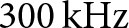 $300\,\mathrm{kHz}$, one of the primary challenges of these chargers is their limited spatial freedom [Reference Varghese, Sealy, Gupta and Pantic10]. To overcome this issue, the AirFuel standard [11] has recently introduced a new operational frequency range centered around
 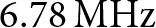 $6.78\,\mathrm{MHz}$, making the devices more robust to misalignment and spatial issues [Reference Li, Qin, Sun and Costinett12].
Operating at these higher frequencies requires more careful design considerations compared to systems functioning in the kHz range. For instance, WPT systems in the kHz range typically use litz wire to mitigate skin and proximity effect losses [Reference Lu and Ngo13]. However, in the MHz range, the effectiveness of litz wire diminishes due to the need for strand diameters significantly smaller than the skin depth [Reference Bartoli, Noferi, Reatti and Kazimierczuk14]. Additionally, litz wire terminations are commonly soldered, which causes the insulation of the strands to melt at the ends, resulting in all strands being conductively connected within the solder. Therefore, the termination itself becomes susceptible to skin effect, leading to non-uniform current distribution. These effects become more pronounced as frequency increases, as shown in [Reference Rosskopf, Bar and Joffe15], and can increase losses. To overcome this issue, coils operating in the MHz frequency range are usually made by printed circuit boards (PCBs) [Reference Schiestl, Brandl, Losch and Starz16–Reference Sun, Muneer, Li and Zhu19].
Another challenge at MHz frequencies is related to the use of compensating capacitors. WPT systems typically operate under resonant conditions to enhance the power transfer efficiency of the inductive coupling, with capacitors connected either in series or parallel with the coils [Reference Buja, Jha, Bertoluzzo and Naik20, Reference Costanzo, Dionigi, Mastri, Mongiardo, Russer and Russer21]. At high frequencies, capacitors can introduce additional losses due to dielectric losses, which become more significant in the MHz range. Furthermore, they may be affected by eddy currents and proximity-effect losses resulting from the magnetic field generated by nearby coil currents [Reference Stein, Kyaw and Sullivan22]. The soldered connections between coils and capacitors can also contribute to losses at these frequencies, and the physical size of the capacitors may increase the overall bulkiness of the system [Reference Qin, Li, Sun and Costinett23]. Moreover, capacitors are additional components that increase system cost and introduce potential points of failure.
To address all these issues, recent studies have leveraged the parasitic capacitance inherent in multilayer PCB designs to create coils that self-resonate at the target operating frequency [Reference Stein, Kyaw and Sullivan22–Reference Wang, Wang, Li, Yang and Hui31]. Moreover, it is worth mentioning that self-resonant coils can also be adopted to achieve compact hybrid inductive and capacitive WPT systems, as shown in [Reference Wang, Yang, Wang and Yang30, Reference Wang, Wang, Li, Yang and Hui31].
The principle behind self-resonant coils is to utilize the parasitic capacitance between conductors to form a series or parallel resonant circuit with the inductance generated by the conductors themselves. Specifically, [Reference Stein, Kyaw and Sullivan22, Reference Stein, Kyaw and Sullivan24] investigate self-resonant parallel-compensated coils, while [Reference Wang, Saket, Troy and Ordonez25] extend the concept by integrating an additional inductor to realize an inductor–capacitor–inductor (LCL) compensation topology. In contrast, [Reference Qin, Li, Sun and Costinett23, Reference Qin, Li and Costinett26–Reference Liu, Yang, Han, Gao, Sun, Wang, Guan and Sun28, Reference Wang, Yang, Wang and Yang30–Reference Fang, Qu, Pong, Lee and Hui32] demonstrate the feasibility of self-resonant series compensation. In the present work, the focus is placed on series compensation, selected for its advantages in WPT systems, including high efficiency and favorable sizing of the power source and the receiving coil [Reference Buja, Jha, Bertoluzzo and Naik20].
In the literature, the design of self-resonant coils is typically based on analytical formulas used to estimate the coil’s capacitance and self-inductance, and thus determine the self-resonant frequency (SRF) [Reference Qin and Costinett29]. This approach has been successfully applied in [Reference Stein, Kyaw and Sullivan22, Reference Wang, Saket, Troy and Ordonez25, Reference Li and Costinett27, Reference Liu, Yang, Han, Gao, Sun, Wang, Guan and Sun28], while in [Reference Qin, Li, Sun and Costinett23, Reference Qin, Li and Costinett26], although analytical models form the basis of the design process, full-wave high-frequency Finite Element Method (FEM) simulations are additionally employed to evaluate the current distribution pattern. While full-wave FEM simulations provide a more accurate analysis of self-resonant coils, they are computationally demanding, which limits their applicability in early design stages. Conversely, analytical formulations allow for rapid evaluations but suffer from reduced accuracy, as they rely on simplified assumptions. In particular, analytical approaches face difficulties in accounting for the influence of the surrounding environment on the equivalent capacitance and inductance of the system and cannot accurately capture the current distribution along PCB traces.
To address these limitations, this work proposes an alternative modeling strategy that couples an FEM electro-quasistatic model, used to evaluate the current distribution across PCB layers and determine the equivalent capacitance, with an FEM magneto-quasistatic model to compute the equivalent inductance. These equivalent parameters are then employed to calculate the SRF at which the system operates. The proposed approach is integrated into an optimization algorithm to tune the coil design parameters and ensure resonance at the target frequency. Although the proposed two-step approach is often adopted in the design of electromagnetic devices, such as in [Reference Torchio33, Reference Marconato and Lucchini34], to the best of the authors’ knowledge, no previous studies have addressed this combined modeling approach for the design of series self-resonant coils in WPT applications.
Furthermore, this work highlights that the current distribution is non-uniform along the copper traces, indicating that not all of the copper is essential for the proper functioning of the system. Indeed, reducing certain portions of the copper trace does not significantly impact the coil’s equivalent impedance. Based on this observation, a parametric analysis is carried out to identify which portions of the traces can be removed without altering the system’s resonant frequency. This leads to the proposal of a novel trace design for self-resonant coils, with the advantage of reduced usage of copper within the system, reducing the cost of the system itself and saving material. To the best of the authors’ knowledge, no previous studies have investigated the impact of copper trace length reduction in the design of self-resonant coils.
The remainder of the paper is organized as follows. The second section provides a general description of the coil used for series self-resonant compensation, which serves as the reference for this study. The third section presents the fundamental concepts of the proposed modeling approach. In the fourth section, the numerical results obtained from the coil design are presented, and a parametric study is conducted to evaluate the potential for copper trace reduction without compromising the coil’s SRF. The fifth section describes the experimental validation of the proposed coil design. The main outcomes of the work are finally summarized in the sixth section.
Coil for series self-resonant compensation
The general structure of the coil implemented in this work is illustrated in Figure 1. It consists of two identical copper traces, each printed on one side of a two-layer PCB. Both traces form planar spiral coils with the same rotational direction and are separated by a dielectric substrate, which has been chosen as FR4 for this application.
Schematic representation of the series self-resonant coil under study.

It is important to note that the two terminals of the coil, labeled A and B in Figure 1, are positioned at opposite ends of the spirals and on opposite PCB layers. This configuration ensures that the current flows in the same direction in both layers, thereby maximizing the coil’s equivalent self-inductance seen from the terminals.
Although there is no physical connection between the two layers, parasitic capacitances are established between the two spiral traces. At low frequencies, the distributed parasitic capacitances between the two layers are a high impedance path, limiting the overall current; whereas when the operating frequency increases, the equivalent distributed impedances related to the parasitic capacitances decrease, and displacement currents through the dielectric become significant. Thus, the overall current value increases [Reference Qin, Li and Costinett26, Reference Zhang, Cheng, Chen, Luo, Zhou, Mai and He35]. As a result, the circuit is closed, and the total current seen from terminal A can flow to terminal B. The same phenomenon occurs in several integrated components, such as L-C-T transformers [Reference Torchio33, Reference Laouamri, Keradec, Ferrieux and Barbaroux36].
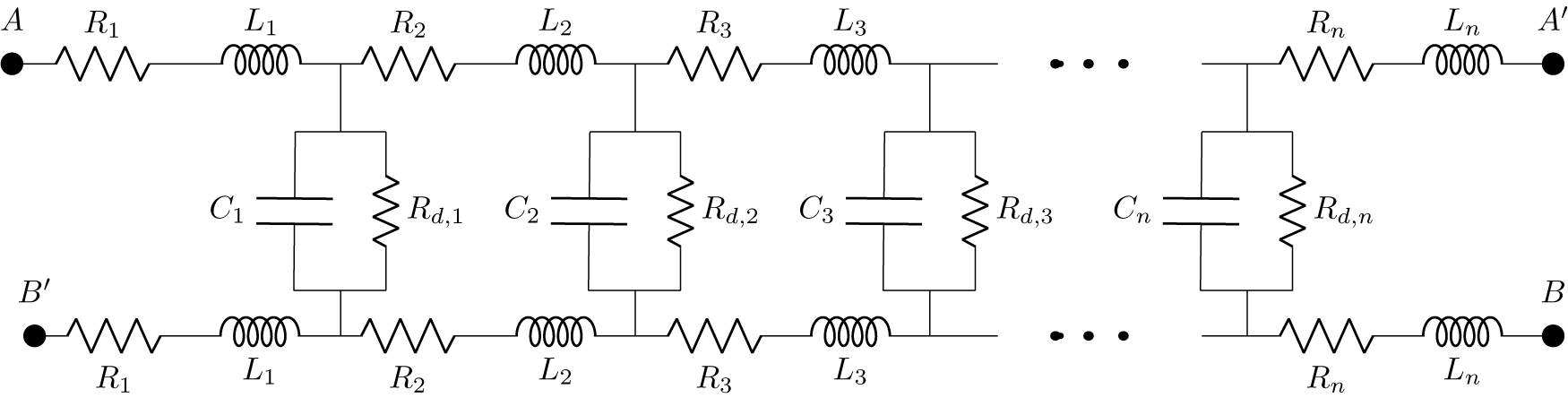
The distributed equivalent circuit model in Figure 2 is a strategy commonly adopted in literature to better visualize and study the behavior of this structure [Reference Qin, Li and Costinett26, Reference Liu, Yang, Han, Gao, Sun, Wang, Guan and Sun28]. The resistances  $R_i$ and the inductances
  $L_i$, with
  $i= 1 \cdots n$, represent the distributed resistance, accounting for the losses along the copper trace, and the distributed inductance of the copper traces, respectively. These values are identical for both traces, as the two spiral copper patterns are geometrically identical. Similarly, the resistances
  $R_{d,i}$ and the capacitances
  $C_i$ represent the distributed resistance of the dielectric, modeling the dielectric losses, and the distributed parasitic capacitance between the two traces, respectively. For simplicity, intra-winding capacitances are neglected, as the parasitic capacitances mainly arise between the copper traces on the two sides of the PCB. This assumption is justified when the copper trace width is larger than the PCB thickness [Reference Fang, Qu, Pong, Lee and Hui32].
Distributed equivalent circuit model.

In particular, Figure 2 illustrates that the extremities of the two copper traces, which do not serve as coil terminals, labeled A ${\prime}$ and B
 ${\prime}$, are effectively open ends. Therefore, it is clear that the current must linearly transition from its nominal value
  $I_0$ at terminal A to zero at A
 ${\prime}$, and conversely, from zero at B
 ${\prime}$ to
  $I_0$ at terminal B in the bottom layer. The current passes from one layer to another as a displacement current through the dielectric layer.
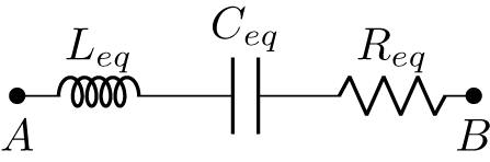
From a circuit perspective, the two-layer PCB coil can be modeled at its terminals as a lumped-parameter series circuit, whose total impedance is expressed as:
 \begin{equation}
Z_{eq}= R_{eq}+j(\omega L_{eq}-\frac{1}{\omega C_{eq}}),
\end{equation}
\begin{equation}
Z_{eq}= R_{eq}+j(\omega L_{eq}-\frac{1}{\omega C_{eq}}),
\end{equation}where  $R_{eq}$ represents the total equivalent resistance accounting for all losses, while
  $L_{eq}$ and
  $C_{eq}$ are the equivalent total values of inductance and parasitic capacitance of the coil, respectively. A schematic representation of the equivalent circuit observed at the coil terminals is provided in Figure 3.
Lumped equivalent series circuit model.

Analytical formulations offer a quick understanding of the system’s behavior, particularly by correlating its geometrical parameters and material properties with the lumped circuit values. In particular, the equivalent capacitance of the system can be approximated analytically, accounting for the edge effects of the conductor, as described in [Reference Li and Costinett27, Reference Liu, Yang, Han, Gao, Sun, Wang, Guan and Sun28]:
 \begin{equation}
C_{eq}= \frac{\varepsilon_r \varepsilon_0l}{h}[w+\frac{h}{\pi}ln\frac{2h}{\pi w}+\frac{h}{\pi}ln (1+\frac{2h}{\pi w}+2\sqrt{\frac{t}{h}+\frac{t^2}{h^2}} )] ,
\end{equation}
\begin{equation}
C_{eq}= \frac{\varepsilon_r \varepsilon_0l}{h}[w+\frac{h}{\pi}ln\frac{2h}{\pi w}+\frac{h}{\pi}ln (1+\frac{2h}{\pi w}+2\sqrt{\frac{t}{h}+\frac{t^2}{h^2}} )] ,
\end{equation}where  $\varepsilon_r$ is the relative permittivity,
  $\varepsilon_0$ is the permittivity of vacuum,
  $h$ is the dielectric thickness,
  $l$ is the total length of one spiral copper trace,
  $t$ is the thickness of the trace, and
  $w$ is the trace width.
Similarly, the equivalent inductance can be determined by the geometric configuration of the single-layer planar spiral coil [Reference Li and Costinett27, Reference Liu, Yang, Han, Gao, Sun, Wang, Guan and Sun28]:
 \begin{equation}
L_{eq}=\dfrac{\mu n^2 d_{avg}}{2}(ln \frac{2.46}{k_u}+0.2k_u^2),
\end{equation}
\begin{equation}
L_{eq}=\dfrac{\mu n^2 d_{avg}}{2}(ln \frac{2.46}{k_u}+0.2k_u^2),
\end{equation}where  $\mu$ is the magnetic permeability,
  $d_{avg}$ is the average diameter,
  $n$ is the number of turns, and
  $k_u = {(d_{out}-d_{in})}/{(d_{out}+d_{in})}$ is the fill ratio.
Although these expressions are approximations, i.e. (2) does not perfectly account for fringing effects [Reference Qin, Li and Costinett26], and (3) relies on layout-dependent coefficients and loses accuracy when spacing between turns increases [Reference Mohan, Hershenson, Boyd and Lee37], they effectively capture the dependence of the equivalent capacitance and inductance on the coil’s geometric parameters. As such, they can be reliably used for early-stage design and estimation. However, the applicability of these formulas is limited to conventional spiral geometries where the spirals on both layers are identical. Consequently, this approach is no longer valid for configurations involving reduced trace coils, as is the scope of this work.
Therefore, it becomes necessary to adopt a more reliable and general modeling approach to accurately tune these geometric dimensions of the coil and design the double-layer structure for achieving a self-resonant configuration, even with unconventional trace shapes.
Electromagnetic model
The design of the coil, and thus the selection of its geometrical dimensions to achieve self-resonance at a target frequency of  $6.78\,\mathrm{MHz}$, is carried out in this work using a 3D FEM model that subsequently adopts two different formulations. Specifically, a 3D electro-quasistatic formulation is employed to evaluate the actual current distribution in the two copper traces, whereas a 3D magneto-quasistatic formulation is adopted to compute the equivalent inductance from the previously obtained current distribution. This two-step decoupling of the simulation process is justified by the negligible radiation effects, given that the coil dimensions are much smaller than the operating wavelength.
In the 3D electro-quasistatic formulation, analyzed in the frequency domain, the current density  $\mathbf{J}$ in the computational domain
  $\Omega$ is given by:
 \begin{equation}
\mathbf{J} = \sigma \mathbf{E} + j\omega \mathbf{D} + \mathbf{J_e},
\end{equation}
\begin{equation}
\mathbf{J} = \sigma \mathbf{E} + j\omega \mathbf{D} + \mathbf{J_e},
\end{equation}where  $\sigma$ denotes the electrical conductivity of the materials,
  $\mathbf{E}$ is the electric field vector,
  $\omega=2\pi f$ is the angular frequency,
  $\mathbf{D} = \varepsilon_r \varepsilon_0 \mathbf{E}$ is the electric displacement field, and
  $\mathbf{J_e}$ is the externally imposed source current density. Here,
  $\varepsilon_r$ denotes the relative permittivity of the material, and
  $\varepsilon_0$ is the vacuum permittivity. This formulation seems to be adequate for describing the current distribution of the system under study, as it accurately captures the displacement current
  $j \omega \mathbf{D}$, which plays a crucial role in the system’s behavior.
The model, implemented and solved using the FEM software Comsol Multiphysics, is driven by externally imposing a known current and voltage at the positive terminal, whose RMS values are indicated with  $I_0$ and
  $V_0$, respectively. The negative terminal is set as the ground reference. The definition and placement of the positive and negative terminals are consistent with those shown in Figure 1.
It is worth noting that, when extracting the equivalent circuit parameters through the proposed two-step approach, the working frequency adopted for the FEM simulation should be sufficiently lower than the expected SRF, as suggested in [Reference Torchio and Lucchini38]. Therefore, a frequency of  $1\,\mathrm{MHz}$ is adopted for the analysis.
From the solution of the electro-quasistatic problem, the capacitive energy  $W_e$ can be extracted and the equivalent capacitance
  $C_{eq}$ between the two traces of the PCB can be evaluated as:
 \begin{equation}
C_{eq} = \dfrac{2W_e}{V_0^2}.
\end{equation}
\begin{equation}
C_{eq} = \dfrac{2W_e}{V_0^2}.
\end{equation} The current density  $\mathbf{J}$ distribution in the two copper traces, obtained from (4), is then used in a 3D magneto-quasistatic problem, solved via the magnetic vector potential
  $\mathbf{A}$ formulation, to compute the equivalent total inductance of the device
  $L_{eq}$ [Reference Marconato and Lucchini34]. This formulation is valid under the assumption that wave propagation phenomena do not occur, which is justified in this case, as the physical size of the coil is much smaller than the electromagnetic wavelength. In particular, this approach is used to compute the magnetic energy
  $W_m$ in the computational domain by solving the equation:
 \begin{equation}
W_m = \frac{1}{2}\int_\Omega \mathbf{A} \cdot \mathbf{J} \ d\Omega
\end{equation}
\begin{equation}
W_m = \frac{1}{2}\int_\Omega \mathbf{A} \cdot \mathbf{J} \ d\Omega
\end{equation}and, therefore, to compute:
 \begin{equation}
L_{eq} = \dfrac{2W_m}{I_0^2}.
\end{equation}
\begin{equation}
L_{eq} = \dfrac{2W_m}{I_0^2}.
\end{equation}Finally, the SRF of the coil is defined as:
 \begin{equation}
SRF = \dfrac{1}{2 \pi \sqrt{L_{eq} C_{eq}}}.
\end{equation}
\begin{equation}
SRF = \dfrac{1}{2 \pi \sqrt{L_{eq} C_{eq}}}.
\end{equation}Coil design and copper trace reduction
The design parameters selected for the optimization process in this work include the inner radius of the spiral  $r_{in}$, the number of turns
  $n$, the trace width
  $w$, and the spacing between adjacent turns
  $s$. The dielectric thickness and the relative permittivity of the substrate are not included as optimization variables, as the dielectric material used in this configuration is standard FR4, commonly employed in PCB manufacturing, with a fixed thickness of
  $1.57\,\mathrm{mm}$ and a relative permittivity of
  $\varepsilon_r = 4.4$. The thickness of the copper trace adopted in this design is
  $35\,{\mu}\mathrm{m}$. It is worth noting that standard FR4 exhibits dielectric losses, which may degrade system efficiency. Furthermore, the copper trace geometry can be optimized to enhance efficiency. Recent studies have therefore explored low-loss dielectric materials and optimized PCB trace geometries to improve the system quality factor [Reference Fang, Qu, Pong, Lee and Hui32, Reference Li, Wu, Yucel and Hui39]. However, since efficiency optimization is not the primary objective of the present work, the substrate material and trace geometry were selected to ensure a conventional and representative PCB implementation. Figure 4 depicts the geometrical parameters considered in the design and optimization process.
Schematic representation of the parameters involved in the optimization and design process.

The tuning of these parameters, to design a coil that resonates at the target frequency of  $6.78\, \mathrm{MHz}$, is performed by means of the Success-History based Adaptive Differential Evolution algorithm (SHADE) [Reference Tanabe and Fukunaga40]. A population size of 10 is employed, with a maximum number of iterations equal to 40. The boundaries of the design variables are reported in Table 1.
Geometrical boundaries of the design variables

The objective function that the algorithm is required to minimize is:
 \begin{equation}
f_{obj} = \dfrac{SRF - SRF_{target}}{SRF_{target}},
\end{equation}
\begin{equation}
f_{obj} = \dfrac{SRF - SRF_{target}}{SRF_{target}},
\end{equation}where  $SRF_{target}$ denotes the desired SRF of
  $6.78\,\mathrm{MHz}$, and
  $SRF$ is the self-resonant frequency of the current coil configuration, computed using the model described in the third section. Therefore, for each individual of the population at each iteration, the two formulations presented above are subsequently solved. The resulting parameters for the coil are then reported in Table 2.
Geometrical parameters of the proposed coil design

The resulting current density distribution in the two copper traces of the proposed coil, obtained from the solution of (4), is shown in Figure 5, where it can be observed that the current is not uniformly distributed across the two layers.
Comparison between the current density distribution in the upper trace (a) and in the bottom trace (b). Current is represented by arrows.

For deeper insight into the system’s behavior, Figure 6 presents the normalized current distribution along the length of the coil. It can be seen that the current in the top layer decreases at the same rate as it increases in the bottom layer, resulting in a symmetrical distribution in which the total current flows exactly through half of the top layer and half of the bottom layer. This behavior aligns with theoretical expectations [Reference Qin, Li and Costinett26], given the assumption that the parasitic capacitance is uniformly distributed along the trace path, meaning all the capacitances  $C_i$ in Figure 2 are equal.
Distribution of the current density (normalized) along the copper trace in the two copper layers.

These results also justify the assumption commonly found in the literature that the total inductance of the coil is equal to the self-inductance of one layer [Reference Liu, Yang, Han, Gao, Sun, Wang, Guan and Sun28]. This is due to the fact that, in each section of the coil, the sum of the current in the two traces is constant and equal to the terminal current  $I_0$.
Accurate information on the actual current distribution within the coil is essential for identifying regions of the copper traces that can be removed without significantly affecting the total inductance and capacitance of the coil. For this purpose, a parametric study on the coil length was conducted to determine which portions of the traces could be eliminated. Specifically, the study focuses on evaluating the angular sector parameter  $\alpha$ of the inner turn of the top layer and the angular sector parameter
  $\beta$ of the outer turn of the bottom layer that can be removed without compromising the electromagnetic performance. Figure 7 indicates a schematic representation of the angular parameters
  $\alpha$ and
  $\beta$ under study. Based on the current distribution along the trace, a maximum value of
  $180^{\circ}$ has been considered for
  $\alpha$, and a maximum value of
  $90^{\circ}$ for
  $\beta$.
Schematic representation of the parameters considered for the trace reduction in the top trace (a) and in the bottom trace (b).

Although the current is close to zero near the open-ended terminals, reaching exactly zero at the terminals themselves, charge accumulation still occurs in these segments of the copper trace. This charge deposition affects the parasitic capacitance of the system. Consequently, any reduction in trace length is expected to modify the SRF of the system. Figure 8 shows the percentage increase in the SRF of the system as the copper trace is reduced according to the parameters described above.
Percentage increase in the SRF of the system due to the copper trace reduction.

The AirFuel standard specifies a nominal operating frequency of  $6.78\,\mathrm{MHz}$ with a tolerance of
  $\pm 150\,\mathrm{kHz}$ [Reference Bonache-Samaniego, Olalla, Martinez-Salamero and Maksimovic41]. Therefore, a maximum increase of 2% in the SRF value is admitted. To ensure compliance with the standard, a target SRF increase of about 1% has been selected. The corresponding values of the adopted angular parameters
  $\alpha$ and
  $\beta$, along with the geometric and electrical characteristics of the proposed coil with reduced trace, are summarized in Table 3. The achieved material reduction is only about 6%, constrained by the requirement to maintain the SRF within the tolerance band prescribed by the standard. Nevertheless, from the authors’ perspective, it is interesting to note that, despite the reduction in the copper trace, the self-inductance of the coil remains unchanged, while the parasitic capacitance decreases slightly.
Geometrical parameters of the proposed reduced copper trace coil design

Experimental results
The two coils, the one with the full copper trace and the one with the reduced copper trace, have therefore been fabricated, and their SRFs have been measured using an Agilent E5071C ENA Vector Network Analyzer (VNA). An SMA connector has been used for the connection to the instrument: the positive terminal of the SMA has been connected to the positive end of the coil on the top layer, while the ground terminal has been connected to the negative end of the coil on the bottom layer. The ground connection has been made by soldering a wire from the coil terminal to the ground pin of the SMA connector. The measurement setup is shown in Figure 9.
Measurement setup.

The two realized coils, the reference one with the full copper trace and the one with the reduced copper trace, are shown in Figures 10 and 11, respectively.
Upper trace (a) and bottom trace (b) of the manufactured coil with full copper trace.

Upper trace (a) and bottom trace (b) of the manufactured coil with reduced copper trace. The reduction is marked in red.

The coil acts as a one-port device, allowing the magnitude of the reflection coefficient  $S_{11}$ to be measured across the desired frequency range using the VNA. The equivalent impedance
  $Z$ of each coil can then be calculated from the reflection coefficient using the relation:
 \begin{equation}
Z = Z_0 \frac{1+S_{11}}{1-S_{11}}
\end{equation}
\begin{equation}
Z = Z_0 \frac{1+S_{11}}{1-S_{11}}
\end{equation}where  $Z_0$ is the reference impedance, with the value of
  $50\,\Omega$.
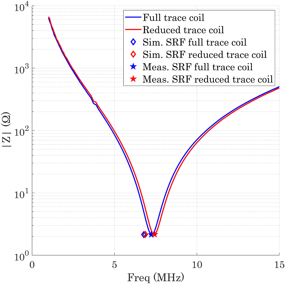
The measured impedance values of the two coils over the frequency range are presented in Figure 12, along with the simulated SRFs. It is interesting to note how the equivalent impedances tend to increase at low frequencies, due to the fact that the coils, when the admittance caused by parasitic capacitive effects is low, behave like open circuits.
Comparison between the measured magnitude of the equivalent impedance along the frequency range for the full trace coil and the reduced trace one.

The frequency at which the equivalent impedance of the coil is lowest can be identified as the SRF of the coil. A more detailed comparison among the SRFs for the two cases, both simulated and measured, is reported in Table 4.
Comparison between measured and simulated SRF values for the two proposed configurations

Along with the SRF, measurements of the equivalent inductance and equivalent capacitance have been provided for both proposed coils. The measurements were performed using a Hioki IM3536 LCR meter at a frequency of  $1\,\mathrm{MHz}$. The results are reported, in comparison with the simulation values, in Tables 5 and 6 for the inductances and capacitances, respectively.
Comparison between measured and simulated inductance values for the two proposed configurations

Comparison between measured and simulated capacitance values for the two proposed configurations

As shown in Table 6, the measured values and the simulated ones are in very good agreement with respect to the capacitance evaluation. Small discrepancies may be due to machining tolerances; in particular, tolerances in the thickness of the FR4 board play a role.
Regarding the self-inductance, a non-negligible relative error between the numerical and experimental results appears. This discrepancy is mainly due to the presence of the wire connecting the negative terminal of the coil to the ground pin of the SMA, which was not included in the simulation. In fact, the current flowing through this wire is in the opposite direction with respect to the current in the spiral on the bottom layer, leading to a reduction in inductance. Moreover, machining defects, such as the scratches visible in Figure 10(a), can also affect the current distribution and therefore the value of the inductance. The relative error in the evaluation of the inductance is also reflected in the evaluation of the SRF.
Since the presence of external wiring can also degrade the performance of the system in terms of efficiency, recent works have discussed the possibility of designing a spiral that allows an easier connection between the spiral and the SMA ground pin, e.g., by considering a counterclockwise spiral for the bottom layer [Reference Qin, Li, Sun and Costinett23]. This solution prevents the reduction of inductance with respect to the simulation values due to the connecting wire, but it reduces the value of the parasitic capacitance. Therefore, a trade-off that is inherent to all engineering processes is required.
Leaving aside the discrepancies between simulated and measured values, and focusing on the difference between the full-trace coil and the reduced-trace one in terms of SRF, it is possible to confirm, both from Table 4 and Figure 12, that the copper-trace reduction affects the final SRF of the system in a negligible way, as previously discussed.
Conclusion
This work addresses the design of a series self-resonant coil for WPT applications, operating at the target frequency of  $6.78\,\mathrm{MHz}$ prescribed by the AirFuel standard. The coil is implemented on a double-layer PCB, with two identical copper traces printed on each side.
A novel methodology combining 3D electro-quasistatic and magneto-quasistatic models is introduced to estimate the equivalent capacitance and inductance of the coil, thereby determining the SRF. The proposed approach achieves accurate SRF prediction while being sufficiently simple to be integrated into optimization algorithms and applied in the early design stage. In addition, it provides detailed insight into the current distribution, revealing a non-uniform pattern along the two layers. This observation is exploited to design a coil with a reduced copper trace length, demonstrating that the SRF, and thus the operating frequency, remains nearly unaffected.
Both the full-trace and reduced-trace coils have been fabricated, and their SRFs have been measured using a VNA, confirming good agreement with simulation results. The reduced-trace design exhibits only a 3% difference in SRF compared to the full-trace configuration, while achieving a reduction in copper usage.
Beyond the proposed application, the main contribution of this work lies in the validation of the design methodology and the demonstration that the copper trace can be reduced without affecting the SRF. Since the proposed approach is general, future work can extend it to higher power density applications, where higher current levels require wider and thicker copper traces. In such cases, a reduction of the copper trace would indeed be significantly more meaningful. Future research will also extend the proposed methodology to include the influence of surrounding materials, such as magnetic flux concentrators, on the behavior of self-resonant coils.
Competing interests
The authors report no conflict of interest.

Giulio Poggiana received the M.Sc. in electrical energy engineering from the University of Padova, Padua, Italy, in 2023. He is currently pursuing the Ph.D. degree in electrical engineering at the University of Padova. From February to July 2025, he was a visiting Ph.D. student at the Laboratoire de Génie Électrique de Paris (GeePs). His research interests include WPT, electromagnetic modeling and simulation, and induction heating.

Riccardo Torchio was born in Padua, Italy, in 1992. He received the M.S. degree in electrical engineering from the University of Padova, Padua, in 2016, and the dual Ph.D. degree in electrical engineering from the University of Padova and Grenoble Electrical Engineering Laboratory (G2ELab), Universitè Grenoble Alpes, France, in December 2019. He is currently with the University of Padova as an Assistant Professor (RTDb). His research interests include numerical methods, optimizations, low-rank compression techniques, uncertainty quantifications, WPT applications, model order reduction, model predictive control, and the development of integral formulations for the study of low- and high-frequency electromagnetic devices.

Lionel Pichon is Senior Researcher (Directeur de recherche) at the CNRS (French National Centre for Scientific Research) in GeePs (Group of electrical engineering of Paris). His research interests include computational electromagnetics, electromagnetic compatibility and WPT. He received the Dip. Eng. from ESIEE-Paris (Ecole Supérieure d’Ingénieurs en Electronique et Electrotechnique) in 1984. In 1985, he joined the Laboratoire de Génie Electrique de Paris (LGEP, now GeePs) where he earned a PhD in electrical engineering in 1989. He got a position at the CNRS in 1989. He is the author or coauthor of more than 130 journal articles in peer-reviewed journals. He is an Associate Editor of the European Physical Journal Applied Physics (EPJ AP) and of the textitJournal of Electromagnetic Waves and Applications.

Mohamed Bensetti received his Master’s degree (DEA) in 2001 and his Ph.D. in Electrical Engineering in 2004 from the University of Paris-Sud, France. From 2005 to 2007, he worked as a researcher at Ecole Supérieure d’Electricité (SUPELEC) – Gif sur Yvette, France. In 2007, he joined Ecole Supérieure d’Ingénieur en Génie Electrique (ESIGELEC), Rouen, where he was a lecturer and researcher in the Research Institute for Electronic Embedded Systems (IRSEEM). In January 2013, he joined the energy department of SUPELEC. He received the «Habilitation à Diriger des Recherches» degree from the University of Paris-Sud in March 2014. He is now a Professor at CentraleSupelec. He is currently with GeePs (Group of electrical engineering, Paris). His current research interests are electromagnetic modeling, electromagnetic compatibility (EMC) and power electronics, and wirless power transmission including modeling, simulation and instrumentation.

Fabrizio Dughiero is a Full Professor of electromagnetic processing of materials (EPM) with Università degli Studi di Padova, Padua, Italy, and the Chief Scientist with the Laboratory of Electroheat, Università degli Studi di Padova.He has been the Founder of a spin-off company (InovaLab) and Unismart Padua Enterprise Ltd., Padua, a new in-house company aimed at developing Technology and Knowledge Transfer of Università degli Studi di Padova. He is currently the Director of the Department of Industrial Engineering, Università degli Studi di Padova. His current research activity, documented by more than 180 scientific publications, mainly deals with theoretical aspects and applications of EPM and electroheat technologies.


 Open access