

I. INTRODUCTION
The abundance of environments that require advanced materials resistant to high temperature, extreme stresses, and other demanding operating conditions has grown rapidly over the past two decades. Reference Beyerlein, Caro, Demkowicz, Mara, Misra and Uberuaga1,Reference Schuster, Ligda, Pan and Wei2 One particular example to that end is the development of fusion as a clean, sustainable energy source, which relies extensively on tungsten for the design of plasma facing components due to its high melting point, good thermal conductivity, high temperature strength, sputtering resistance, and chemical compatibility with tritium. Reference Zinkle and Snead3 A number of strategies focused on alloy design have been pursued for enhancing the performance of tungsten for extreme environment applications. Reference Wurster, Baluc, Battabyal, Crosby, Du, García-Rosales, Hasegawa, Hoffmann, Kimura, Kurishita, Kurtz, Li, Noh, Reiser, Riesch, Rieth, Setyawan, Walter, You and Pippan4 Refining of the grain size to the ultrafine and nanocrystalline regimes, in particular, has demonstrated promising results for collectively enhancing the mechanical performance Reference Hao, Fan, Zhang, Luo, Wang, Liu and Fang5,Reference Wei, Jiao, Ramesh, Ma, Kecskes, Magness, Dowding, Kazykhanov and Valiev6 and defect accommodation under ion irradiation. Reference Wurster and Pippan7,Reference El-Atwani, Hinks, Greaves, Gonderman, Qiu, Efe and Allain8 Unfortunately, the far-from-equilibrium state occupied by nominally pure nanocrystalline metals renders them thermally unstable, Reference Suryanarayana and Koch9 and nanostructured tungsten suffers from the same limitation at elevated temperatures. Reference Chookajorn, Murdoch and Schuh10
Thermal instabilities in nanocrystalline metals derive from the energetic penalty associated with the introduction of a high volume fraction of grain boundaries, Reference Weissmuller11 which promotes grain growth at low homologous temperatures to reduce the total grain boundary area and in turn the system free energy. Reference Malow, Koch and Bourrell12,Reference Ames, Markmann, Karos, Michels, Tschope and Birringer13 A classic example of this phenomenon is found in nanocrystalline Ni where grain size increased by 20× at only 30% of its melting point. Reference Hibbard, McCrea, Palumbo, Aust and Erb14 Similar behavior has been observed across a range of single-component nanocrystalline metals such as cobalt, Reference Hibbard, Aust, Palumbo and Erb15 iron, Reference Riotino, Antonione, Battezzati and Marino16 copper, Reference Simoes, Calinas, Vieira, Vieira and Ferreira17 and silver Reference Dannenberg, Stach, Groza and Dresser18 where microstructural evolution often prescribes to curvature-driven grain growth with the grain boundary velocity, ν, proportional to the local mean curvature of the boundary, κ:
 $$\nu = {M_{{\rm{gb}}}} \times {\gamma _{{\rm{gb}}}} \times \kappa \quad ,$$
In Eq. (1), M gb is the grain boundary mobility and γgb the grain boundary energy, Reference Burke and Turnbull19 which capture the kinetic and thermodynamic components of grain growth, respectively. Grain growth in single-component nanocrystalline metals has been modeled using Eq. (1) and demonstrated that an enhanced grain boundary mobility is accompanied by a reduced activation energy for grain growth. Reference Ames, Markmann, Karos, Michels, Tschope and Birringer13,Reference Simoes, Calinas, Vieira, Vieira and Ferreira17,Reference Natter, Schmelzer, Loffler, Krill, Fitch and Hempelmann20 However, the onset of microstructural evolution in a range of nanocrystalline metals often transpires through an abnormal growth process, which has been observed in copper, Reference Brons and Thompson21,Reference Gertsman and Birringer22 nickel, Reference Brons and Thompson21,Reference Kacher, Robertson, Nowell, Knapp and Hattar23 iron, Reference Paul and Krill24 palladium, Reference Ames, Markmann, Karos, Michels, Tschope and Birringer13 and cobalt Reference Hibbard, Aust, Palumbo and Erb15 as well as a number of binary nanocrystalline alloys. Reference Dake and Krill25–Reference Hibbard, Aust and Erb27 As the average grain size increases from the nanocrystalline to the ultrafine grain regime, abnormal grain growth widely succumbs to curvature-driven mechanisms, Reference Klement and Da Silva28 thus underscoring the importance of stabilizing the nanostructure collectively against the initial and late stages of grain growth in nanocrystalline metals.
Abnormal grain growth has been attributed to a number of factors such as nonuniform grain boundary mobility, Reference Kim and Park29 second-phase particles inhibiting grain boundary migration, Reference Koju, Darling, Kecskes and Mishin30 and surface energy anisotropy in thin films. Reference Thompson31 In the absence of second-phase particles, the onset of abnormal grain growth follows the mean field theory of Rollett and Mullins Reference Holm, Miodownik and Rollett32 and derives from nonuniform grain boundary mobility relating to the interplay between grain boundary properties and local network effects from the surrounding grain structure. Reference Garcia, Tikare and Holm33 Local pinning of the grain boundaries also augments their mobility due to a number of factors such as grain boundary faceting, Reference Abdeljawad, Medlin, Zimmerman, Hattar and Foiles34,Reference Lee, Hwang, Yoon and Henry35 surface energy-driven thermal grooving in thin films, Reference Frost, Thompson and Walton36 and the presence of second-phase particles in alloys. Reference Koju, Darling, Kecskes and Mishin30 The latter has been explored in nanocrystalline Cu–Ta Reference Darling, Roberts, Mishin, Mathaudhu and Kecskes37 and Au–Pt Reference Abdeljawad, Lu, Argibay, Clark, Boyce and Foiles38 systems, which exhibited solute-rich nanoprecipitates that inhibit grain boundary migration at temperatures exceeding 50% of the respective melting points for each alloy. Grain boundary solute enrichment also has thermodynamic implications for nanostructure stability where reductions in the interfacial free energy due to grain boundary segregation can suppress or effectively eliminate the driving force for grain growth. Reference Weissmuller11,Reference Trelewicz and Schuh39,Reference Liu and Kirchheim40 The propensity for solute to segregate to the grain boundaries in a particular alloy system is captured by the ratio of the enthalpy of segregation to the heat of mixing, Reference Murdoch and Schuh41 which has important implications for the stability of the microstructure.
A direct comparison of solute distribution and thermal stability was accomplished in the nanocrystalline iron system employing Mg and Cu as alloying elements. Reference Clark, Hattar, Marshall, Chookajorn, Boyce and Schuh42 The Fe–Mg system exhibited stable nanocrystalline grain structures with Mg segregation to the grain boundaries while Fe–Cu exhibited a phase-separated microstructure with limited grain boundary segregation and more extensive grain growth, which aligned with predictions from lattice Monte Carlo modeling. These principles have also been investigated in tungsten alloys with a stability map constructed by Chookajorn et al. Reference Chookajorn, Murdoch and Schuh10 from which Ti was identified as a potential candidate for producing a nanocrystalline-stable material. An alloy of W–20 at.% Ti synthesized via high energy ball milling exhibited an as-milled grain size of approximately 20 nm that remained stable at 1100 °C for one week Reference Chookajorn and Schuh43 ; unalloyed nanocrystalline tungsten coarsened by over an order of magnitude to a grain size of >0.5 µm under identical conditions. Similar behavior has been observed in a range of other alloy systems including W–Cr Reference Chookajorn, Park and Schuh44 and Hf–Ti Reference Polyakov, Chookajorn, Mecklenburg, Schuh and Hodge45 as well as in nanocrystalline ceramic materials such as La-doped yttria-stabilized zirconia (YSZ). Reference Dey, Chang, Gong, Liu and Castro46
In this study, thermal stability of magnetron sputtered nanocrystalline tungsten and tungsten alloy thin films is explored through in situ transmission electron microscopy (TEM) annealing experiments up to 1000 °C. Abnormal grain growth and its transition to a continuous, curvature-driven growth process in unalloyed nanocrystalline tungsten are first characterized by tracking the evolution of select grains as a function of annealing temperature in bright-field TEM images. Insights into the mechanisms facilitating discontinuous grain growth are then provided by considering the interplay between phase transitions, texture, surface energy effects, and grain boundary misorientation distributions. To combat microstructural instabilities that lead to the early onset of grain coarsening, solute additions are investigated in the W–Ti and W–Cr binary alloy systems. Grain size distributions following heat treatment at 1000 °C are compared to understand the implications of alloy selection for thermal stability, and finally discussed in the context of the underlying solute distributions quantified through scanning transmission electron microscopy (STEM) and electron energy loss spectroscopy (EELS) measurements.
II. MATERIALS AND METHODS
Magnetron sputtered W, W–20 at.% Ti, and W–15 at.% Cr thin films were deposited in an AJA ATC-1500 stainless-steel chamber from >99.95% pure elemental targets obtained from the Kurt J. Lesker company (Jefferson Hills, Pennsylvania). The films were deposited to a nominal thickness of 20–30 nm on polished NaCl substrates acquired from International Crystal Laboratories (#0002A-4549; Garfield, New Jersey). Prior to deposition, the substrates were heated to 150 °C for 1 h to remove surface water. The sputtering chamber was evacuated to <6.66 × 10⁻⁶ Pa before flowing in ultrahigh purity argon to a pressure of 0.266 Pa at a rate of 10 standard cubic centimeters per minute. Films were deposited at 100 °C and subsequently cooled to ambient temperature prior to removal from the chamber. Deposition rates, measured from the total film thickness via small angle X-ray reflectivity Reference Sasanuma, Mamoru, Okada, Yamamoto, Kitano and Ishitani47 using an X’Pert Philips X-ray diffractometer (Philips, Almelo, the Netherlands) operated with a Cu Kα source at 45 kV and 40 mA, ranged from 0.12 to 0.18 nm/s depending on composition.
In situ annealing of the unalloyed nanocrystalline tungsten films used a Hummingbird ETEM 1500 series heating holder (Hummingbird Scientific, Lacey, Washington) in a JEOL JEM 2100 TEM (JEOL Ltd., Tokyo, Japan). Films were heated at a rate of 5 °C/min to 300, 450, 550, and 650 °C where they were held for 5–10 min before being cooled to room temperature over a 1 h period. Precession electron diffraction (PED) was conducted on the annealed films using the NanoMEGAS ASTAR mapping system (NanoMEGAS SPRL, Brussels, Belgium). All scans underwent an ambiguity and noise reduction, which included the removal of anomalous spikes and a zero-solution extrapolation. In situ annealing of the nanocrystalline tungsten alloy films was conducted up to 1000 °C using a Gatan heating holder (Model #628; Gatan, Inc., Pleasanton, California) in a Philips CM30 TEM (Philips, Hillsboro, Oregon) operated at 300 kV. The temperature was manually ramped to 1000 °C where upon the films were held for 20 min prior to cooling over a 1 h period. Images and videos of these films were acquired by the TVIPS (TVIPS GmbH, Gauting, Germany) and Gatan Digital Micrograph software (Gatan Inc., Pleasanton, California), respectively. Image and video analysis was performed using ImageJ (U.S. National Institute of Health, Bethesda, Maryland), Adobe Photoshop, and Adobe Premier (Adobe Systems, San Jose, California) with grain orientation maps produced via the Oxford Tango software package (Oxford Instruments, Abingdon, England).
Phase analysis was conducted by generating radial intensity plots from the selected area electron diffraction patterns where the intensity was integrated over all azimuthal angles as a function of distance from the center of the direct beam, which was converted to Bragg angles using a wave length of 0.0273 Å. Reference Detor and Schuh48 Phase indexing used the method described by Edington Reference Edington49 that compares the ring spacing ratios to the reciprocal of the known ratio of d-spacings for all possible crystal structures of interest. Solute distributions in the alloys were characterized using a Hitachi HD2700C STEM (Hitachi, Ltd., Tokyo, Japan) equipped with a Gatan high-resolution Enfina detector (Gatan Inc., Pleasanton, California) at the Center for Functional Nanomaterials at Brookhaven National Laboratory. High angle annular dark field (HAADF) imaging in conjunction with EELS were used to map Ti and Cr solute additions based on their known electron binding energies Reference Williams and Thompson50 of 455 and 574 eV, respectively, relative to 1809 eV for W. EELS was selected for its enhanced resolution of small features, which is ideal for correlating elemental segregation to grain boundaries in the TEM. Reference Egerton51
III. MICROSTRUCTURAL EVOLUTION IN NANOCRYSTALLINE TUNGSTEN THIN FILMS
In this section, microstructural evolution in sputter-deposited nanocrystalline tungsten thin films is described at temperatures up to 650 °C. In situ approaches enabled real-time imaging of the nanostructure through annealing, which was complemented with post-mortem PED and grain tracking analyses to uncover transitions in the growth mechanisms as a function of temperature. The as-deposited tungsten film exhibited a nanocrystalline grain structure as evident in the bright-field image in Fig. 1(a), and from the corresponding grain size distribution in Fig. 1(b), the mean grain size of the as-deposited film was 10 ± 3 nm. The electron diffraction pattern contained a large number of distinct spots indicative of a nanocrystalline state. Indexing of this diffraction pattern produced the normalized integrated radial intensity profile in Fig. 1(c), which revealed a two-phase structure containing metastable β-tungsten with the A-15 cubic structure Reference Okeefe and Grant52 mixed with BCC α-tungsten. The α-phase was primarily detected through the appearance of reflections at high Bragg angles; however, other peaks are likely present at low diffraction angles but not evident due to the overlap with the higher intensity β-tungsten reflections. The presence of the metastable β-phase is common in tungsten thin films deposited via magnetron sputtering, Reference Vullers and Spolenak53 and its implications for microstructural evolution and thermal stability are explored in the remainder of this section.
(a) Bright-field TEM image of the as-deposited nanocrystalline tungsten film with the selected area diffraction pattern shown in the inset, (b) corresponding grain size distribution with a mean grain size of approximately 10 nm, and (c) integrated radial intensity profile determined from the inset in (a) revealing a two-phase structure composed primarily of metastable β-tungsten and BCC α-tungsten appearing at higher Bragg angles.

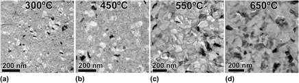
Initial coarsening of the nanostructure transpired through a discontinuous growth process where a subset of grains grew heterogeneously at 300 °C as evident in the bright-field image shown in Fig. 2(a). The resulting bimodal grain structure, evident in the grain size histogram of Fig. 3(a), contained a distribution of large nanocrystalline grains embedded within the nanocrystalline matrix retained from the as-deposited state with a mean grain size of 30 ± 30 nm; this large standard deviation was attributed to the bimodal distribution of grain sizes. As shown in Fig. 2(b), a similar grain structure was observed upon heating to 450 °C, and changes were not qualitatively discernible in the size or distribution of the larger nanocrystalline grains. The mean size from the histogram was 30 ± 26 nm, which was consistent with the results at 300 °C. However, the number fraction of larger nanocrystalline grains (i.e., with size greater than 20 nm) increased by 29%, which was attended by a 5% decrease in the relative fraction of smaller grains occupying the initial nanocrystalline matrix. A further increase in the temperature to 550 °C produced a conspicuous increase in the number of larger grains that evolved from the small grained nanocrystalline matrix as evident in Fig. 2(c). This manifested as an increase in the mean grain size to 48 ± 33 nm that was accompanied by an additional 22% increase in the fraction of larger grains and a 19% reduction in the fraction of the smaller nanocrystalline grains from the histogram in Fig. 3(a). The bimodal grain structure eventually succumbed to a unimodal nanocrystalline structure at 650 °C shown in Fig. 2(d) with a mean grain size of approximately 87 ± 25 nm, thus signaling a transition to a continuous grain growth process.
Bright-field images of the nanocrystalline tungsten films at (a) 300 °C, (b) 450 °C, (c) 550 °C and (d) 650 °C. The as-deposited unimodal nanocrystalline structure evolved to a bimodal distribution of grain sizes at the intermediate annealing temperatures, ultimately converging back to a unimodal grain structure at 650 °C.

(a) Grain size distributions for the annealed tungsten films delineated for the bimodal grain size distributions at intermediate annealing temperatures and unimodal nanocrystalline structure at 650 °C. Normalized grain size as a function of the initial grain size for the tracking of individual grains over the temperature ranges of (b) 300–450 °C and (c) 450–650 °C. The size of the outlined grains remained consistent for the temperature range in (b) whereas curvature-driven grain growth transpired over the higher temperature range in (c).
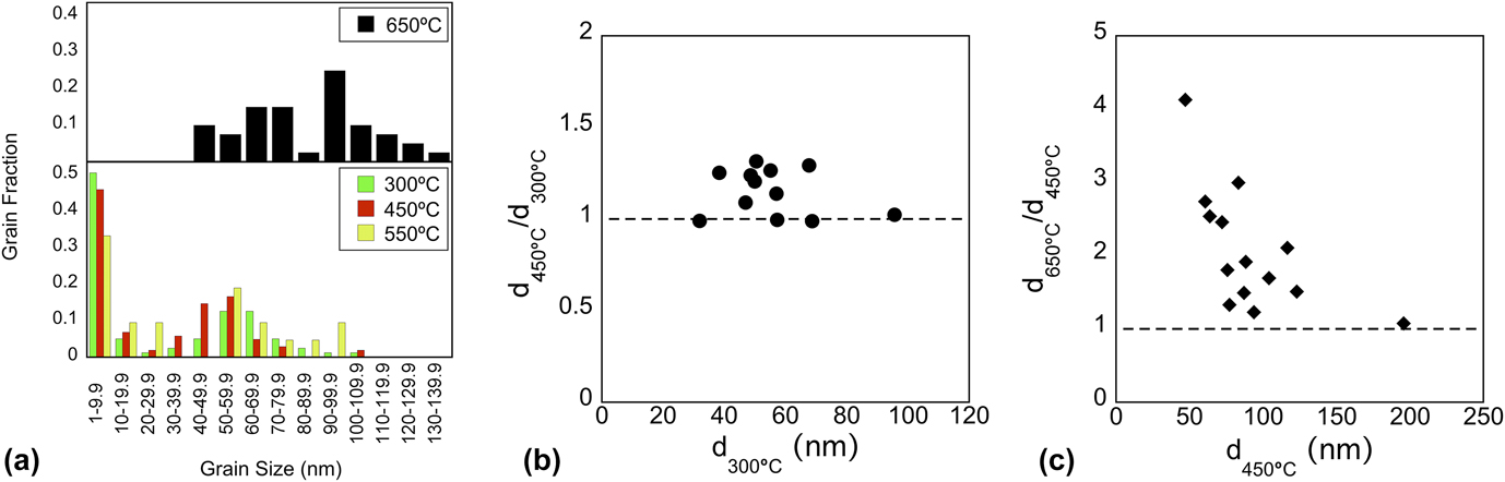
The evolution of individual grains was tracked at temperatures of 300, 450, and 650 °C to confirm the transition from abnormal to continuous grain growth. A subset of larger grains embedded in the as-deposited nanocrystalline matrix was first outlined at 300 °C, and the corresponding grains were mapped in the bright-field image during heating to 450 °C. The individual sizes of the mapped grains were measured at both temperatures, and the ratio of grain sizes are plotted as a function of the original grain size at 300 °C in Fig. 3(b). The tracked grains exhibited very limited growth over the temperature range of 300–450 °C as evidenced by the grouping of the data points around unity across all initial grain sizes spanning the range of 20–80 nm. Combined with the increase in the number fraction of larger nanocrystalline grains from Fig. 3(a), microstructural evolution was dominated by abnormal grain growth at temperatures up to 450 °C. Results from mapping of individual grains over the second temperature range of 450–650 °C are depicted in Fig. 3(c) normalized and plotted against the initial grain size of each mapped grain at 450 °C. An inverse relationship emerged where smaller nanocrystalline grains exhibited accentuated growth relative to the larger grains spanning the range of 50–200 nm, which is the characteristic of curvature-driven grain growth and substantiates the transition to continuous grain growth in the nanocrystalline tungsten films.
Phase evolution during the abnormal and continuous grain growth regimes was explored through analysis of the selected area electron diffraction patterns corresponding to the bright-field images at temperatures of 300, 550, and 650 °C in Fig. 2, and the resulting normalized integrated radial intensity profiles are depicted in Figs. 4(a)–4(c), respectively. At 300 °C near the onset of abnormal grain growth, the film retained the two-phase structure from the as-deposited state as evidenced by the presence of reflections for both the metastable β-phase and BCC α-phase. Increasing the temperature to 550 °C produced a significant increase in the intensities of the BCC α-tungsten peaks in Fig. 4(b) while only a single (321) reflection remained for the β-phase. The emergence of α-tungsten as the predominant phase in the α–β film was attributed to an allotropic transformation of the metastable β-phase, which aligned with the increase in the number fraction of larger nanocrystalline grains and attendant decrease in the relative fraction of the small nanocrystalline grains from the as-deposited state. The transition to continuous grain growth at 650 °C was accompanied by a complete transformation of the films to BCC α-tungsten as evidenced by the absence of β reflections in Fig. 4(c). Collectively, these results suggested that the allotropic phase transition was central in contributing to the formation of bimodal grain size distributions through abnormal grain growth, which ultimately converged to a unimodal grain structure upon completion of this phase transformation process.
Integrated radial intensity profiles acquired at temperatures of (a) 300 °C and (b) 550 °C on the bimodal nanocrystalline structures during abnormal grain growth and at (c) 650 °C upon convergence to a unimodal nanocrystalline structure. The α–β two-phase tungsten film evolved to single-phase BCC α-tungsten through an allotropic phase transformation.

The coupling between allotropic phase transformations and microstructural evolution through discontinuous grain growth has been demonstrated in nanocrystalline cobalt where face centered cubic (FCC) α-Co grains with sizes greater than 100 nm emerged discontinuously in the as-deposited hexagonal close packed (HCP) ε-Co nanocrystalline matrix with an average grain size of 13 nm. Reference Hibbard, Palumbo, Aust and Erb54 Similarly in the as-deposited nanocrystalline tungsten films composed largely of β-tungsten, a thermodynamic driving force existed for this metastable phase to transform to the equilibrium BCC α-phase, Reference Okeefe and Grant52 which was in competition with a large driving force for grain growth. Consequently, phase and microstructural instabilities were inherently coupled in the nanocrystalline tungsten films with the phase transition driving discontinuous grain growth, which is in good agreement with the observations in nanocrystalline cobalt as well as a range of other materials. Reference Dake and Krill25,Reference Xiao, Cheng and Jin26,Reference Brewer, Follstaedt, Hattar, Knapp, Rodriguez and Robertson55 We finally note that in cobalt, the addition of 1.1 at.% P shifted the allotropic phase transition and concomitant onset of abnormal grain growth to higher temperatures, Reference Choi, da Silva, Klement, Al-Kassab and Kirchheim56 thus suggesting that alloying can stabilize nanocrystalline materials against sudden losses in thermal stability due to discontinuous coarsening events.
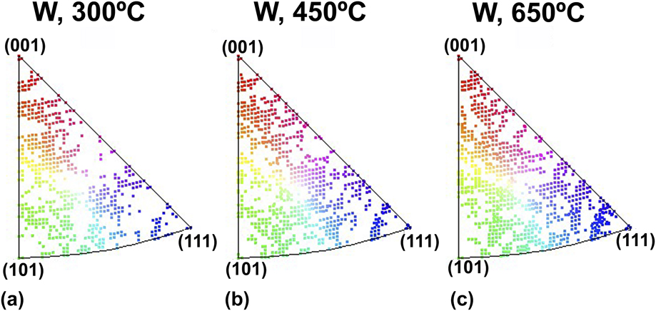
Film texture has also been demonstrated to augment thermal stability in nanocrystalline nickel thin films by locally constraining grain growth and in turn, producing bimodal grain size distributions Reference Kacher, Hattar and Robertson57 that are similar to the grain structures observed in the nanocrystalline tungsten thin films. To probe the effect of crystallographic orientation through the abnormal and continuous growth regimes, grain orientation and combined reliability-orientation maps were acquired at temperatures of 300, 450, and 650 °C via PED and are depicted in Figs. 5(a)–5(c) colored according to the corresponding inverse pole figures in Figs. 6(a)–6(c). Measurements in the as-deposited nanocrystalline matrix that contained grain sizes ≤10 nm exhibited low reliability due to the difficulty in resolving orientation for grains sizes in this range via PED. Reference Brons and Thompson58 Consequently, only those grains within the reliability threshold during discontinuous grain growth were incorporated into the orientation analysis. The combined reliability-orientation maps exhibited random grain orientations, which was substantiated in Fig. 6 where each point on the inverse pole figures corresponded to an individual grain from the PED maps in Fig. 5. The uniform distribution of grain orientations apparent at each temperature is characteristic of a random polycrystalline texture, and indicates that no preferential grain orientations emerged during the abnormal or continuous growth regimes.
Precession electron diffraction orientation maps (upper) and combined reliability-orientation maps (lower) at (a) 300 °C, (b) 450 °C, and (c) 650 °C. Grains are colored according to the IPFs in Fig. 6, and the black regions in the reliability-orientation maps capture the low reliability index for grains ≤10 nm in size within the smaller grain size nanocrystalline matrix. The reader is referred to the web version of this article for interpretation of references to color.

Inverse pole figures for the combined reliability-orientation maps in Fig. 5 at (a) 300 °C, (b) 450 °C, and (c) 650 °C. Each point corresponds to the orientation of an individual grain and employs an identical coloring scheme. A random polycrystalline texture was apparent across all temperatures indicating that no preferential orientations emerged during the abnormal or continuous growth regimes. The reader is referred to the web version of this article for interpretation of references to color.
Two additional caveats relating to the role of surface energy and nonuniform grain boundary mobility in the onset of abnormal grain growth are finally noted. Surface energy effects in thin films are known to produce thermal grooving at the intersection of grain boundaries with the film surface, Reference Mullins59 which has been connected to local pinning of the boundaries Reference Thompson31,Reference Sachenko, Schneibel and Zhang60 and the growth of grains through a discontinuous process. Reference Frost, Thompson and Walton36 Given that the nanocrystalline tungsten films were appreciably thin (i.e., 25–30 nm), surface energy effects likely contributed to the onset of abnormal grain growth and the rate at which metastable β transformed to the equilibrium α-phase. Nonuniform grain boundary mobility has been explored in the context of grain boundary energy Reference Holm, Hassold and Miodownik61–Reference Gruber, Miller, Hoffmann, Rohrer and Rollett63 with implications for the formation of anisotropic grain boundary character distributions. Reference Dillon and Rohrer64 In nanocrystalline Ni, abnormal grain growth has been attributed to the preferential migration of high-mobility coincident site lattice (CSL) boundaries. Reference Brons and Thompson21 Boundary fractions could not be quantified for the bimodal structures due to the aforementioned reliability issues; however, analysis of the boundary fractions from Fig. 5(c) revealed a uniform distribution of low-energy CSL boundaries in the unimodal grain structure, which is consistent with prior grain growth studies in nanocrystalline metals. Reference Kacher, Robertson, Nowell, Knapp and Hattar23,Reference Brons and Thompson65 Surface energy and nonuniform grain boundary mobility effects thus likely complemented the allotropic phase transformation in driving initial microstructural evolution through abnormal grain growth and its transition to continuous, curvature-driven growth upon convergence to a unimodal nanocrystalline structure.
IV. SOLUTE STABILIZATION AGAINST ABNORMAL GRAIN GROWTH
Nanocrystalline tungsten thin films exhibited an allotropic phase transformation at low homologous temperatures that was coupled with abnormal grain growth, and the transition to continuous grain growth above 550 °C coincided with complete transformation of the metastable β-phase to the equilibrium BCC phase of tungsten. The effect of solute additions on the as-deposited state of tungsten and stabilization of its nanostructure against abnormal grain growth is described in this section at temperatures up to 1000 °C. Thin films of W–20 at.% Ti and W–15 at.% Cr were sputter deposited using identical deposition procedures to the unalloyed nanocrystalline tungsten films. These particular alloy compositions were selected based on their propensity to produce nanocrystalline stable states as predicted from the regular nanocrystalline solution model, Reference Chookajorn, Murdoch and Schuh10 which has been demonstrated in both systems using powder metallurgy techniques. Reference Chookajorn and Schuh43,Reference Chookajorn, Park and Schuh44 Our analysis focuses on mapping nanostructure stability collectively with solute distributions in as-deposited and heat treated thin film samples using in situ TEM annealing combined with STEM-EELS analysis.
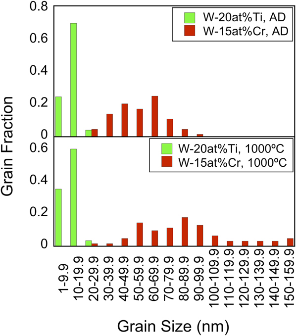
Sputter deposition of W–20 at.%. Ti produced the nanocrystalline grain structure shown in Fig. 7(a) with a mean grain size of 14 ± 4 nm from the histogram in Fig. 8 for the as-deposited condition. This structure remained stable through in situ TEM annealing of the film at 1000 °C as evident in Fig. 7(b), and was reflected in the mean grain size exhibiting only a subtle increase to 18 ± 4 nm in the histogram. The W–15 at.% Cr film also exhibited a nanocrystalline grain structure in the as-deposited state as shown in Fig. 7(c), but with a larger initial grain size of 55 ± 17 nm from the histogram in Fig. 8. It was difficult to ascertain qualitative changes to the grain structure in Fig. 7(d) upon annealing of the W–Cr film; however, the mean grain size in the histogram evolved to 86 ± 31 nm, corresponding to a 56% increase from the as-deposited grain size. The grain boundaries in the bright-field image in Fig. 7(d) also appeared brighter relative to the intragranular regions of the film, which was attributed to thickness contrast. The emergence of locally thin regions coinciding with the grain boundaries suggests that annealing promoted the formation of grain boundary voids, gaps, and/or grooving.
Bright-field images and selected area diffraction patterns for the nanocrystalline tungsten alloy thin films including (a) as-deposited W–20 at.% Ti, (b) 1000 °C annealed W–20 at.% Ti, (c) as-deposited W–15 at.% Cr, and (d) 1000 °C annealed W–15 at.% Cr.

Grain size distributions for the W–20 at.% Ti and W–15 at.% Cr alloys in the as-deposited state (upper) and following heat treatment at 1000 °C (lower). A shift to larger nanocrystalline grain sizes was apparent in the W–Cr alloy and indicative of grain growth whereas the W–Ti alloy exhibited little change in the overall grain size distribution.
Both alloy films exhibited significantly enhanced thermal stability relative to their unalloyed counterpart, and the addition of alloying elements eliminated abnormal grain growth with microstructural evolution instead transpiring solely through continuous grain growth. In unalloyed tungsten, this transition aligned with transformation of the metastable β-phase to the stable BCC α-phase of tungsten. A phase analysis was conducted on the alloy films in the as-deposited and annealed conditions, and the integrated radial intensity profiles are shown in Fig. 9. In the as-deposited state, predominant α-tungsten reflections were evident in both the W–20 at.% Ti and W–15 at.% Cr films in Figs. 9(a) and 9(c), respectively. The addition of alloying elements in solid solution thus eliminated the formation of the metastable β-phase and in turn, stabilized the α-phase in thin film nanocrystalline tungsten. The appearance of subtle shoulders on the (110) and (310) reflections toward lower Bragg angles of the W–Cr film suggested that some small amount of a Cr-rich phase was present; however, quantitative indexing of these peaks was difficult due to their low intensity and overlap with the α-tungsten reflections. Annealing of the films produced distinguishable Ti and Cr peaks in Figs. 9(b) and 9(d), respectively, which indicated that a solute-rich second phase precipitated within the tungsten solid solution during the 1000 °C anneal of both alloy films.
Integrated radial intensity profiles from the selected area electron diffraction patterns in Fig. 7 for (a) as-deposited W–20 at.% Ti, (b) 1000 °C annealed W–20 at.% Ti, (c) as-deposited W–15 at.% Cr, and (d) 1000 °C annealed W–15 at.% Cr. The emergence of Ti and Cr peaks in (b) and (d), respectively, indicated that solute-rich second-phases formed upon annealing at 1000 °C.

Previous studies on alloys of nominally identical composition produced via high-energy ball milling uncovered the formation of a heterogeneous solute distribution upon annealing with some noteworthy distinctions between W–Ti Reference Chookajorn and Schuh43 and W–Cr. Reference Chookajorn, Park and Schuh44 In the W–Ti system, Ti-depleted regions were detected following an 1100 °C heat treatment that were comparable to the grain size, suggesting that the Ti atoms were segregated to the grain boundaries. Conversely, Cr-rich nanoscale precipitates were identified predominantly at the grain boundaries upon annealing at 950 °C, and an increase in temperature to 1400 °C produced a duplex nanostructure containing both Cr-rich grains and Cr segregation to the grain boundaries. Our data provides an opportunity to understand the implications of heterogeneous solute distributions for the grain size stability as the deposition and annealing conditions were identical for both alloy compositions.
STEM measurements were used to map the distribution of the solute-rich phases in the alloy films leveraging HAADF imaging collectively with EELS analysis to correlate solute distributions with underlying microstructural features. The HAADF image of the as-deposited W–Ti film is shown in Fig. 10(a) with the corresponding elemental map produced from the EELS scan also depicted. The Z-contrast in the HAADF image indicates that compositional inhomogeneities were present in the as-deposited W–Ti film, which was confirmed in the EELS map from the selected region of the HAADF image. Annealing of the W–Ti film amplified this solute partitioning as evidenced in Fig. 10(b). The spatial distribution of Ti in the as-deposited and annealed films was commensurate with the grain size, thus suggesting Ti segregation to the grain boundaries. A heterogeneous solute distribution was also detected in the as-deposited W–Cr film in Fig. 11(a); however, it was difficult to ascertain whether the Cr-rich regions aligned with the grain boundary network. A noticeable change in the solute distribution was uncovered upon annealing of the W–Cr film at 1000 °C. The EELS map in Fig. 11(b) demonstrated extended Cr-rich regions that coincided with the finest grain sizes in the tail of the distributions of the annealed film in Fig. 8, i.e., for grain sizes <40 nm. The appearance of Cr-rich grains also aligned with the emergence of conspicuous Cr reflections in the selected area electron diffraction pattern.
HAADF images and EELS maps for the W–20 at.% Ti film in the (a) as-deposited and (b) 1000 °C annealed conditions. The EELS maps correspond to the outlined region in the HAADF image in (a) and from the entire image in (b). The as-deposited films exhibited subtle grain boundary segregation, which became more pronounced following heat treatment.

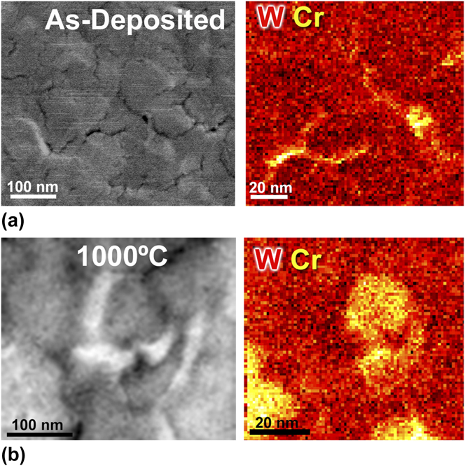
HAADF images and EELS maps for W–15 at.% Cr film in the (a) as-deposited and (b) 1000 °C annealed conditions. The EELS maps were produced from the entire HAADF images. The as-deposited films exhibited subtle grain boundary segregation whereas Cr-rich regions were detected upon annealing.
Solute distributions in the sputter-deposited films were consistent with the aforementioned results on nanocrystalline tungsten alloys of nominally identical composition albeit synthesized through high-energy ball milling. Reference Chookajorn and Schuh43,Reference Chookajorn, Park and Schuh44 Compositional inhomogeneities exhibited spatial distributions commensurate with characteristic microstructural length scales, indicating the presence of grain boundary segregation as well as solute-rich grains particularly in the W–Cr system. Similar solute dependent grain character distributions have been observed in the phase separating Fe–Cr system and correlated to grain boundary excess volume and energetics in the presence of solute atoms. Reference Zhou, Yu, Kaub, Martens and Thompson66 Solute-rich nanostructured second phases constitutes a unique class of nanocrystalline metals referred to as nanoduplex alloys. Relative to “classical” nanocrystalline alloys stabilized through grain boundary segregation, nanoduplex alloys evolve to a different equilibrium state containing multiple nanostructured phases governed by configurational entropy contributions, and are thus referred to as entropically stabilized alloys. Reference Xing, Kalidindi and Schuh67 In these systems, less solute is available to segregate to the grain boundaries due to the presence of a solute-rich second phase, and it consequently becomes more difficult to effectively stabilize the nanocrystalline grains against thermal coarsening. This was manifested in the sputter-deposited W–Cr films as enhanced grain growth relative to the W–Ti system where solute-rich grains were absent in the EELS mapping. The reduced thermal stability of the sputter-deposited W–Cr films relative to W–Ti can therefore be attributed to a shift in the grain boundary segregation state in the presence of a solute-rich second phase, which underscores the role of grain boundary chemistry in solute-stabilized nanocrystalline alloys.
V. CONCLUSIONS
Microstructural evolution in nanocrystalline tungsten thin films composed primarily of the metastable β-phase was explored through in situ TEM annealing experiments. At temperatures below 550 °C, grain growth transpired through a discontinuous process in turn producing a bimodal grain size distribution containing large nanograins dispersed in the initial small grained nanocrystalline matrix. Abnormal grain growth was coupled to an allotropic phase transformation of metastable β to BCC α-tungsten, which aligned with previous observations of grain growth in nanocrystalline metals with competing microstructural and phase instabilities. The convergence to a unimodal nanocrystalline structure at 650 °C signaled a transition to continuous, curvature-driven grain growth that was accompanied by complete transformation of the films to BCC α-tungsten. The addition of alloying elements Ti and Cr eliminated the formation of the metastable β-phase and in turn, stabilized the α-phase in the as-deposited tungsten alloy films. Both alloys exhibited significantly enhanced thermal stability relative to their unalloyed counterpart up to 1000 °C, and the addition of alloying elements eliminated abnormal grain growth with microstructural evolution instead transpiring through a continuous growth process. Compositional inhomogeneities exhibited spatial distributions that were commensurate with characteristic microstructural length scales, indicating the presence of grain boundary segregation. Solute-rich grains were also present in the W–Cr films and their reduced thermal stability relative to W–Ti was attributed to a shift in the grain boundary segregation state due to the emergence of a solute-rich second phase, thus underscoring the role of grain boundary chemistry in the design of solute-stabilized nanocrystalline alloys.
ACKNOWLEDGMENTS
Support for this work was provided for OKD and JRT by the National Science Foundation through Grant DMR-1410941 with additional support from the Stony Brook University-Brookhaven National Lab Seed Grant Program. TK and GBT acknowledge support from the Army Research Office through Grant W911NF1310436 and KH from the Materials Science and Engineering Division of the Department of Energy Office of Basic Energy Sciences. The authors gratefully acknowledge Dr. Lihua Zhang of Brookhaven National Laboratory for assistance with the STEM-EELS measurements and Dr. Brittany Muntifering of Sandia National Laboratories for her guidance on the PED analysis. The authors would also like to thank Dr. Fadi Abdeljawad of Sandia National Laboratories for his valuable insights and feedback. TEM was conducted using resources of the Center for Functional Nanomaterials, Brookhaven National Laboratory, which is supported by the U.S. Department of Energy, Office of Basic Energy Sciences under Contract No. DE-SC0012704. Sandia National Laboratories is a multimission laboratory managed and operated by National Technology and Engineering Solutions of Sandia, LLC., a wholly owned subsidiary of Honeywell International, Inc., for the U.S. Department of Energy’s National Nuclear Security Administration under contract DE-NA-0003525.


 Open access