Introduction
The development of the display industry has experienced different stages from the cathode ray tube [Reference Blasse and Bril1], liquid crystal display [Reference Channin and Carlson2], and plasma display panel [Reference Meunier, Belenguer and Boeuf3] to the light-emitting diodes (LEDs) [Reference Burroughes, Bradley, Brown, Marks, Mackay, Friend, Burns and Holmes4]. Due to the excellent properties of organic luminescent materials such as high efficiency, high contrast, fast response time, and wide viewing angle, organic LED (OLED) is becoming the dominant trend for the next-generation display technology [Reference Reineke, Lindner, Schwartz, Seidler, Walzer, Lüssem and Leo5, Reference Adachi, Nagai and Tamoto6]. Light would emit from the polymer or small organic molecules (such as TPP [Reference Su7], Alq3 [Reference Curioni, Boero and Andreoni8], TBADN [Reference Jarikov and Kondakov9], anthracenes [Reference Kido, Hongawa, Okuyama and Nagai10]) directly in OLED display [Reference Pope, Kallmann and Magnante11, Reference Tang and VanSlyke12]. Besides, the OLED device can be fabricated on plastic substrates, which is compatible with the flexible electronics [Reference Kim, Han and Noh13, Reference Abbel, de Vries, Langen, Kirchner, t’Mannetje, Gorter, Wilson and Groen14]. However, the organic emitting layer, as well as the metal electrodes, is easy to be eroded by the water and oxygen in the ambient [Reference Ghosh, Gerenser, Jarman and Fornalik15], leading to the degradation of the OLEDs. Glass or metal lids were used to encapsulate the devices with the edge area sealed by the ultraviolet curable glue, which presented superior barrier properties. The lack of flexibility made it difficult to be applied to the flexible displays. Hence, thin film encapsulation (TFE) has emerged as an attractive method to fabricate the flexible barriers [Reference Park, Chae, Chung and Lee16, Reference Vera and Moro17].
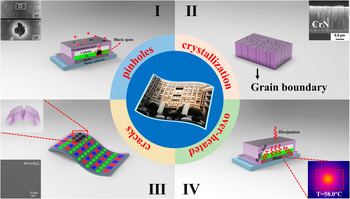
For OLED encapsulation, the adhesion and conformality of the barrier films are of great importance to guarantee the reliability and stability. Among various physical vapor deposition (PVD) methods, the magnetron sputtering and ion plating have been developed to address poor adhesion. Yet, these high energy methods often lead to the damage of OLED surfaces. Moreover, the conformality of PVD methods is also hard to be promoted. The chemical vapor deposition (CVD) could provide films with stronger adhesion and better conformality than that of PVD. These high-temperature deposition processes are not compatible with the thermal budget of the organic light-emitting layer. Hereby, plasma-enhanced chemical vapor deposition (PE-CVD) has been developed to lower the process temperature and becomes the dominant TFE method. But the unavoidable pinholes on the surfaces [Reference Keuning, van de Weijer, Lifka, Kessels and Creatore18] lead to moisture permeation into the electrodes and emitting layers, as shown in Fig. 1(I) [Reference Uchida and Yamashita19]. At the same time, the thicker layer tends to crystallize [Reference Miikkulainen, Leskelä, Ritala and Puurunen20, Reference Wan, Zhang, Lee, Yang, Choi, Han, Kim and Kwon21], and the grain boundaries would serve as the pathway for the moisture permeation, as shown in Fig. 1(II). The above issues will lead to the black spots of the light-emitting areas. Thus, the thickness of inorganic barriers needs to be controlled precisely at nanoscale to suppress the pinholes and grain boundaries. Method to solve these issues is to deposit different materials alternatively to suppress the crystallization [Reference Chou, Yu, Tseng, Hsu, Shyue, Wang and Tsai22], and the pinholes would be decoupled effectively. On the other hand, the internal stress originated from the increasing thickness of the barrier films as well as the external stress accumulated lead to the crack or delamination of barriers from the OLED surfaces [Reference Jen, Bertrand and George23, Reference Ylivaara, Liu, Kilpi, Lyytinen, Schneider, Laitinen, Julin, Ali, Sintonen, Berdova, Haimi, Sajavaara, Ronkainen, Lipsanen, Koskinen, Hannula and Puurunen24, Reference Lewis25, Reference Jen, George, McLean and Carcia26], which is shown in Fig. 1(III). In the Barix method invented by Vitex system [Reference Burrows, Graff, Gross, Martin, Hall, Mast, Bonham, Bennett, Michalski, Weaver, Brown, Fogarty and Sapochak27], the polymer is utilized to help decouple the pinholes and release the stress, and the barrier property of the inorganic/organic dyads is equivalent to that of glass lids. Nevertheless, the manufacturing of OLEDs needs to be transferred between different vacuum chambers, making it high cost to be adopted in the large area and high-throughput manufacturing. Besides, the OLED faces serious performance degradation due to heat accumulation that damages the luminescent materials [Reference Kwon, Kim, Im, Bae, Chang, Park and Choi28], leading to the decrease in the efficiency and lifetime [Reference Vamvounis, Aziz, Hu and Popovic29, Reference Moore and Shi30, Reference Park, Ham and Park31]. Thus, when designing the encapsulation layer, the following issues need to be considered: (i) the pinhole-decoupled and water-resistant barriers without grain boundaries need to be fabricated to promote the barrier property when applied in the severe conditions with high temperature and high humility; (ii) the overall structure needs to be optimized to release the internal or external stress applied on the barriers, which can promote the mechanical property when applied to flexible OLEDs; (iii) the thermal conductivity should be taken into account to avoid the thermal degradation of OLEDs during the continuous usage; (iv) the transparent barriers need to be fabricated with low-temperature process to promote the performance of OLEDs, and the cleanliness of the chambers should be guaranteed to avoid the particle contamination, which may damage the barriers; and (v) the higher deposition rate is necessary for the commercial applications with mass production.
Different degeneration paths of the barrier structures: (a) black spots aroused by the pinholes, (b) grain boundaries as the permeation paths, (c) cracks of the barrier structures, and (d) over-heated caused by poor thermal conductivity.

Atomic layer deposition (ALD) is known to be a powerful ultrathin film fabrication method based on the time-sequenced self-limiting reactions, and the film thickness and uniformity can be controlled precisely even when applied to the large-area substrates [Reference Steven32]. The densely packed and pinhole-free ALD-based films can be deposited directly on the devices through low-temperature processes, and the conformal films can be utilized as high-quality barriers for organic devices [Reference Short, Pamidi, Bloomberg, Li and Losego33, Reference Duan, Yang, Chen, Ye and Liu34, Reference Lee, Han, Lee, Baek and Park35]. In this review, different ALD-based approaches are introduced to solve the specific problems shown in Fig. 1, including the monolayer films, composite structures, and inorganic nanolaminates, which can inhibit the pinholes and crystallization, and the optical transmittance can be tuned to promote the performance of OLEDs. To eliminate the cracking through the stress, the polymers or oxides with reversal residual stress are combined to improve the barrier flexibility. Meanwhile, the location of the neutral axis (NA) can be optimized to reduce the strain applied to the fragile layers. Furthermore, the materials with high thermal conductivity are inserted to transport the heat out of the devices, which can protect the emitting layer from thermal aging. Besides, the ALD reactors and processes for TFE are also reviewed. Finally, the future development of the ALD methods for the TFE of OLEDs is also discussed.
Monolayer and composite structures
To suppress the black spots aroused by the pinholes of the barrier layers, different materials and deposition methods, including thermal evaporation, CVD, and sputtering, have been utilized to obtain the densely packed encapsulation structures, and the preparation processes and structures have been optimized by the experimental or simulation methods.
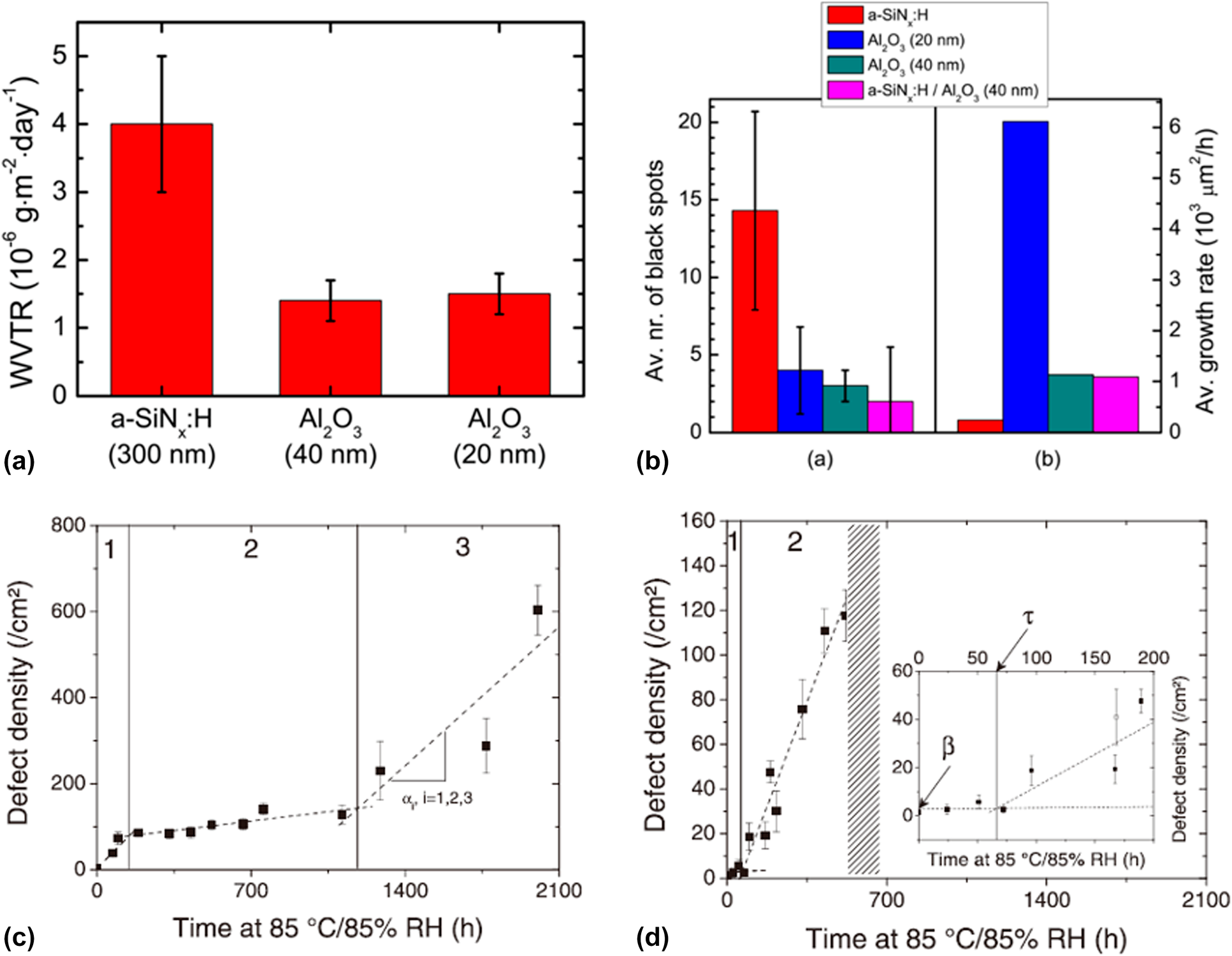
Similar to the glass lid, the constricted interstitial spaces of the Si–O lattice can block the moisture diffusion effectively [Reference Tropsha and Harvey36], but the high-temperature process of SiOx via CVD limits its application in OLEDs [Reference Ahn, Kim, Kang, Im and Lim37, Reference Lee, Choi, Shong, Oh and Park38, Reference Burton, Boleslawski, Desombre and George39]. George and colleagues reported that the SiNx layer could be fabricated at low temperature via PE-CVD, but it has poor barrier property, and it was speculated that the lower density columnar boundaries in SiNx layer may present pathways for moisture [Reference Ovanesyan, Hausmann and Agarwal40, Reference Park, Kim, Heo and Kim41, Reference Carcia, McLean, Groner, Dameron and George42]. Similar result was found in SiOx films prepared via thermal evaporation [Reference Maindron, Jullien and André43]. Thus, great attention has been paid to the ALD method due to its unique assets. Among the various dielectrics prepared via ALD method, Al2O3 is the most studied material due to the superior barrier property. In the deposition processes of trimethylaluminum (TMA) and H2O (deionized water), the excessive precursors and by-products methane are hard to be removed out of the ALD chamber due to the low deposition temperature, resulting in incomplete chain reaction and increasing voids [Reference Steven32, Reference Li, Gao, Li, Zhou, Zou, Tao, Wang, Xu and Peng44]. Duan and colleagues utilized the computational fluid dynamics to calculate the amount of species absorbed on the substrate surfaces [Reference Yang and Duan45, Reference Holmqvist, Törndahl and Stenström46, Reference Lide and Haynes47], and a longer purge time was adopted to remove the excessive precursors and by-products (Table I, line 10). With the optimized process parameters, the water vapor transmittance rate (WVTR) of 70-nm-thick Al2O3 obtained at 80 °C improved to 10−2 g/m2·day, and similar result was also reported by Carcia and colleagues [Reference Groner, George, McLean and Carcia48]. To increase the density to lower down the WVTR of Al2O3 films further, Yang et al. replaced the H2O with O3 as the oxidant with a shorten purge time due to the lower viscosity of O3 than H2O [Reference Yong-Qiang, Yu, Ya-Hui, Xiao, Ping, Dan, Feng-Bo and Kai-wen49], resulting in a higher deposition efficiency (Table I, line 11). Besides, the O3 with higher reactivity can consume the TMA more sufficiently [Reference Yang, Duan, Chen, Sun, Duan, Wang and Yang50, Reference Duan, Sun, Yang, Chen, Yang, Duan and Wang51]. An improved hydrophobic property of the O3-based Al2O3 films was revealed via the water contact analysis, and the barrier property was two orders of magnitude higher than that of H2O-based Al2O3 film. Duan and colleagues revealed that the transient steric hindrance in low-temperature deposition process caused by the by-product gas molecules would block part of the active sites on the substrates, which prevented the reactions with the precursors [Reference Wang, Wang, Xu, Liu, Chen, Chen, Hu and Duan52]. Therefore, the H2O-based Al2O3 films contained a large number of unreacted –CH3 groups and O3-based films left more carbon-based impurities [Reference Wang, Liu, Liu, Chen, Xiong, Xu, Chen, Li and Duan53]. Hence, the multiple short pulse process was adopted to reduce the transient steric hindrance. In this way, the oxidant precursor will be injected into the chamber twice in one cycle, which is separated with a purge process, and the active sites can be consumed completely. Similarly, Peng and colleagues reported that the Al2O3 films prepared by the H2O and O3 in turn in one cycle as oxidants performed higher density and purity, leading to the superior barrier property [Reference Li, Gao, Li, Zhou, Zou, Tao, Wang, Xu and Peng44] (Table I, line 14). Besides, Hoffmann et al. utilized the plasma-enhanced atomic layer deposition (PE-ALD) to improve the film quality [Reference Yun, Ko and Lim54, Reference Hoffmann, Theirich, Pack, Kocak, Schlamm, Hasselmann, Fahl, Räupke, Gargouri and Riedl55, Reference Franke, Baumkötter, Monka, Raabe, Caspary, Johannes, Kowalsky, Beck, Pucci and Gargouri56], and the Al2O3 films showed an ultralow WVTR value of 10−6 g/m2·day (Table I, line 13).
Summary of the WVTR values of monolayer.
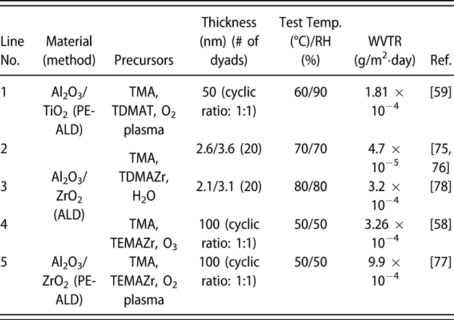
The investigations of the monolayers such as ZnO2 and ZrO2 have also been carried out. Choi and colleagues prepared pure ZnO and doped ZnO films, and the real-time resistance changes of them at 85 °C/85% relative humidity (RH) were monitored [Reference Kwon, Jeon and Choi57]. The measurement results indicated that the doped ZnO film had more corrosion resistance than the pure ZnO layer. It revealed that the degradation of the electrical conductivity of pure ZnO layer was due to the higher potential energy barrier when the –OH groups chemisorbed along the grain boundary, which agreed well with the transmission electron microscope (TEM) result. However, in the doped ZnO film, the Al and Mg dopants could substitute the Zn and hinder the crystallization. Oh et al. prepared the Al2O3 and ZrO2 monolayers with the same thickness of 100 nm, which corresponded to the WVTRs of 7.05 × 10⁻⁴ and 3.87 × 10⁻³ g/m2·day [Reference Oh, Shin, Park, Ham and Jeon58], respectively (Table I, line 20). The high-resolution transmission electron microscope (HR-TEM) was utilized to obtain the structural information about the ZrO2 film, the growth of which followed the [111] direction, and the grain boundaries acted as the permeation path. Similar results have been reported in the monolayers of TiO2 [Reference Kim, Kim, Park, Jeong, Kim, Chung, Kim and Park59], MgO [Reference Kwon, Jeon, Choi, Park, Kim and Choi60, Reference Kim, Han, Kim, Choi, Im and Bae61], etc. The processes and barrier properties of the monolayer structure via ALD are summarized in Table I.
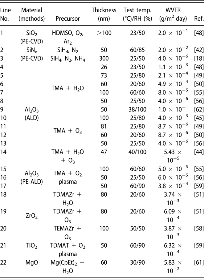
The performance of the OLEDs encapsulated with monolayer and composite structures has been investigated. Kessels and colleagues counted the growth behavior of the black spots on the OLEDs encapsulated with different structures at 20 °C/50% RH. As shown in Fig. 2(a), the Al2O3 layer has better barrier property than the SiNx layer [Reference Park, Chae, Chung and Lee16]. Besides, the black spot density of SiNx was much higher than that of others after long time storage, as shown in Fig. 2(b), and a higher average growth rate of black spots was found in the Al2O3 layer due to uncovered large defects. In addition, the barrier resistance of the composite Al2O3/SiNx structure improved significantly compared with the monolayers [Reference Park, Oh, Hwang, Lee, Yang and Chu62, Reference Park, Oh, Hwang, Lee, Yang, Chu and Kang63]. The pinholes and low-density columnar boundaries could be sealed up effectively via ALD method [Reference Carcia, McLean, Groner, Dameron and George42]. Maindron et al. investigated the occurrence and growth mechanism of the black spots of nonfluorescent tris-(8-hydroxyquinoline) aluminum (AlQ3) in the accelerated conditions [Reference Maindron, Jullien and André43]. It was found that the barrier structures containing Al2O3 layer presented a lag time τ due to the pinhole-free property of the ALD-based Al2O3 films, after which the defect densities started to increase significantly. The observation results of SiOx and Al2O3 are shown in Figs. 2(c) and 2(d). The black spot occurrence rates were decomposed into different regimes (numbered 1, 2, and 3), and the hatched area in Fig. 2(d) represents the total fluorescence failure of the device, where the inset means the enlarged data plots in 0–200 h time range. Park and colleagues revealed that the harsh environment (high temperature and humidity) made the encapsulation layers deteriorating to the porous “flowerlike” structure [Reference Kim, Kim, Park, Jeong, Kim, Chung, Kim and Park59]. After the lag time, the growth rate of the black spot number increased rapidly due to the corrosion of Al2O3 [Reference Pasieczna-Patkowska and Ryczkowski64], leading to a higher growth rate of defect density for Al2O3 film than that of SiOx film in regime 2. When coating the Al2O3 film with SiOx, the longest lag time and slowest growth rate of the defect density were obtained compared with those of other structures.
(a) Intrinsic WVTR values measured for a-SiNx:H (PE-CVD) and Al2O3 (PE-ALD) films; (b) average number and the average growth rates of black spots on OLED samples encapsulated with different structures; and defect density evolution versus storage time for device encapsulated with (c) evaporated SiO2 layer and (d) Al2O3 layer.
Inorganic nanolaminates
As mentioned above, the oxide films such as ZnO [Reference Kim, Hwang, Park and Yun65, Reference Zhang, Wang, Murakami and Song66], TiO2 [Reference Mitchell, Attard and Triani67], and ZrO2 [Reference Duan, Sun, Yang, Chen, Yang, Duan and Wang51, Reference Hausmann and Gordon68] tend to crystallize with the increasing thickness, and the grain boundaries would serve as the pathway for the moisture to permeate into the devices, resulting in the degradation of the OLED displays. To further decrease the thickness and suppress the crystallization of the barrier structures, great attention has been paid to the laminated structures.
Based on the activated rate theory, a simple empirical model for the change in permeation mechanism of laminated structures is deduced as below [Reference Tropsha and Harvey36], where P com denotes the permeation rate of the overall structure and P 1, P 2, etc., mean the permeation rates of sublayer 1, 2… respectively.
 $${P_{{\rm{com}}}} = {\left[ {{1 / {{P_1} + {1 / {{P_2} + }}{1 / {{P_3} + \cdots }}}}} \right]^{ - 1}}\quad .$$
This ideal series assumes that each component is continuous, and the interfaces between each component are not low-energy conduits to transport. However, the theory is not consistent with the entire experimental results due to the imperfection of the sublayers, and the permeation mechanism in the laminated structures needs to be clarified with in-depth researches.
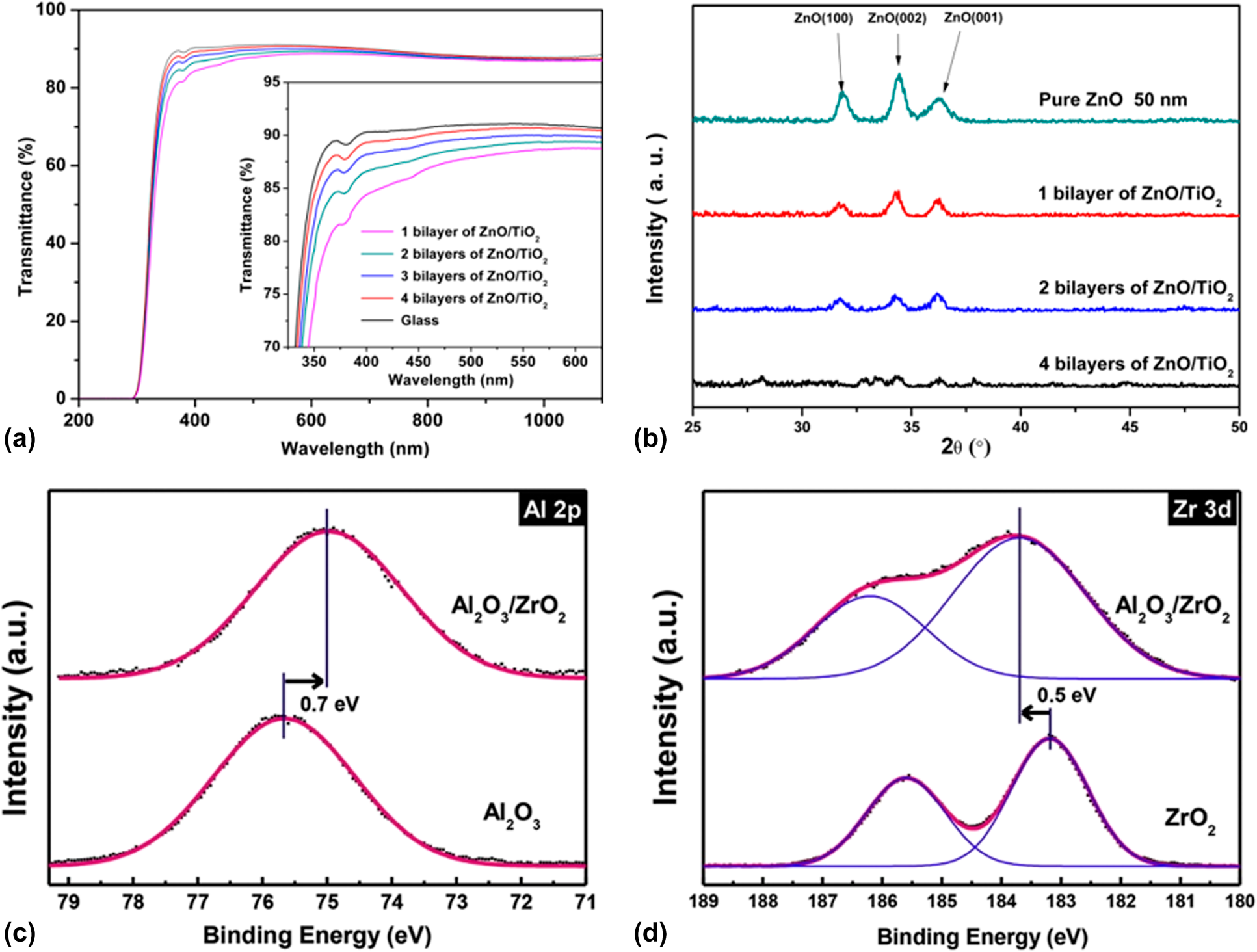
Prior to the activated rate theory [Reference Tropsha and Harvey36], the barrier property of the encapsulation structure improves with the increase in the sublayer numbers. However, the thicker the inorganic barriers are, the less flexible they are. Besides, the repeated transfer process in different vacuum chambers leads to particle contamination [Reference Ueno, Konishi and Azuma69], resulting in the destruction of the barriers. Attentions have been focused on the nanolaminates prepared via ALD method, which can be obtained in one chamber continuously [Reference Ylivaara, Kilpi, Liu, Sintonen, Ali, Laitinen, Julin, Haimi, Sajavaara, Lipsanen, Hannula, Ronkainen and Puurunen70, Reference Viter, Baleviciute, Abou Chaaya, Mikoliunaite, Balevicius, Ramanavicius, Zalesska, Vataman, Smyntyna, Gertnere, Erts, Miele and Bechelany71]. As shown in Fig. 3(a), we reported that the optical property of ZnO/TiO2 nanolaminates (such as refractive index and transparency) could be tuned by adjusting the number of sublayers with the thickness of overall structure maintained constant [Reference Chen, Lin, He, Duan, Qi, Wang and Shan72]. Besides, the increasing number and decreasing thickness of sublayers lead to the amorphous structure of the barriers according to the XRD patterns shown in Fig. 3(b). Similar results were reported by George and colleagues, and the electrical and mechanical properties could also be adjusted [Reference Iatsunskyi, Coy, Viter, Nowaczyk, Jancelewicz, Baleviciute, Załęski and Jurga73, Reference Elam, Sechrist and George74]. Meyer et al. reported the Al2O3/ZrO2 nanolaminates as ultrahigh gas-diffusion barriers; the barrier performance of which improved 1–2 orders of magnitude compared with that of the Al2O3 layer in the accelerated condition of 70 °C/70% RH [Reference Meyer, Görrn, Bertram, Hamwi, Winkler, Johannes, Weimann, Hinze, Riedl and Kowalsky75] (Table II, line 2). The low-temperature deposition process led to the incomplete precursor reaction, which agreed well with the Fourier transform infrared spectroscopy (FTIR) results [Reference Meyer, Schneidenbach, Winkler, Hamwi, Weimann, Hinze, Ammermann, Johannes, Riedl and Kowalsky76]. The amorphous Al2O3 hindered the crystallization of ZrO2 in the Al2O3/ZrO2 nanolaminates. Besides, the ZrO2 layer could prevent the accumulation of unreacted Al–OH species and the formation of extended voids in the Al2O3 sublayers, increasing the packing density. Besides, Jeon and colleagues demonstrated the formation of ZrAlxOy-aluminate phase at the interfaces via the X-ray photoelectron microscopy characterization [Reference Lee, Choi, Shin, Park, Ham, Jung and Jeon77, Reference Meyer, Schmidt, Kowalsky, Riedl and Kahn78] (Table II, lines 3 and 5), which is shown in Figs. 3(c) and 3(d). The Al 2p core level was shifted toward a lower binding energy, and the Zr 3d core level was shifted toward a higher binding energy. Taking the electronegativity of Al (1.61) and Zr (1.33) into consideration, Zr tend to donate an electron and Al tend to gain an electron to form a strong chemical bonding. Juhong et al. even obtained the pure ZrAlxOy phase structure by conducting Al cycle and Zr cycle alternatively, which performed the best barrier property [Reference Oh, Shin, Park, Ham and Jeon58] (Table II, line 4).
(a) Transmittance of ZnO/TiO2 laminates at different bilayers’ number on glass substrate; (b) grazing incidence X-ray diffraction of the as-deposited ZnO/TiO2 laminates; X-ray photoelectron spectroscopy (XPS) spectra of Al2O3, ZrO2, and ZrAlxOy phase of (c) Al 2p and (d) Zr 3d core levels.
Summary of the barrier properties of nanolaminates.
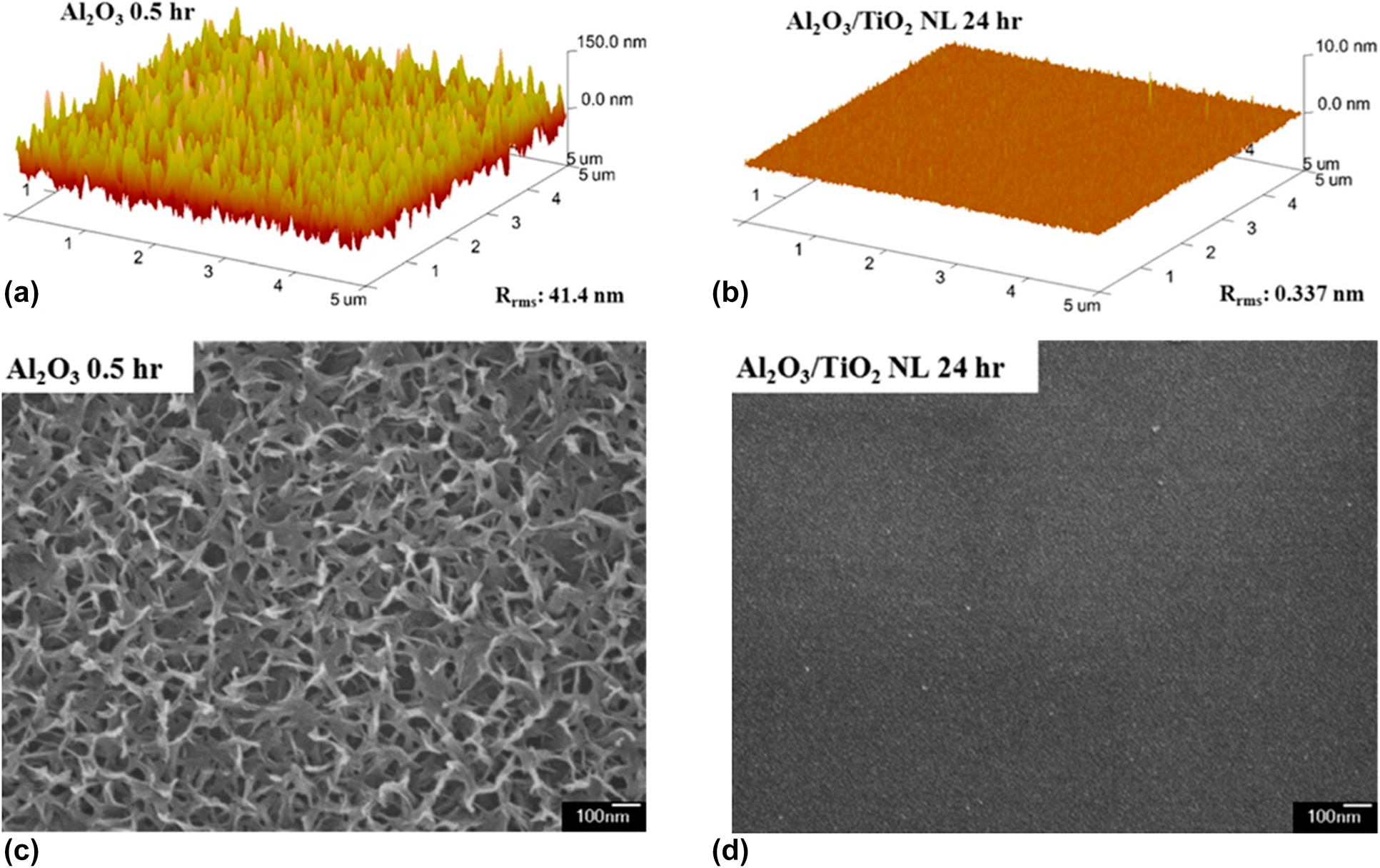
Similar to the Al2O3/ZrO2 system, Lae et al. prepared the Al2O3/TiO2 nanolaminates by conducting the Al cycle and Ti cycle alternatively [Reference Kim, Kim, Park, Jeong, Kim, Chung, Kim and Park59] (Table II, line 1). The Al2O3 monolayer and Al2O3/TiO2 nanolaminates were immersed in water at 90 °C for 30 min, and the topography of the samples was characterized by atomic force microscopy (AFM) and field-emitting scanning electron microscopy (FE-SEM). As shown in Fig. 4, the surface roughness increased significantly and petal structures were formed for the individual Al2O3 layer. In contrast, the surface of the nanolaminates remained smooth, which demonstrated the excellent water–corrosion-resistant property of the TiAlxOy-aluminate phase. Similar results could be found for Al2O3/SiO2 [Reference Choi, Kim, Park, Park, Jeong, Choi, Song, Lee, Kim and Ju79, Reference Dameron, Davidson, Burton, Carcia, McLean and George80], ZnO/HfO [Reference Chou, Yu, Tseng, Hsu, Shyue, Wang and Tsai22] nanolaminates, and the barrier properties of different nanolaminate encapsulation structures are listed in Table II.
AFM images of the surfaces of the (a) single Al2O3 and (b) Al2O3/TiO2 nanolaminate films after immersion in water at 90 °C; FE-SEM photographs of the surfaces of (c) single Al2O3 and (d) Al2O3/TiO2 after immersion in water at 90 °C.
Hybrid structured TFEs under mechanical stresses
The inorganic barrier structures carry intrinsic mechanical residual stress, and the stress increases with the increasing thickness of the overall structures [Reference Tripp, Stampfer, Miller, Helbling, Herrmann, Hierold, Gall, George and Bright81]. Besides, when combined with the external stress caused by bending or stored in the harsh environment, the barrier layer tends to crack or delaminate from the device surface, leading to the degradation of the OLEDs. To make the barrier structures more flexible and to maintain the excellent barrier property, the hybrid laminated structures with mechanical design and polymers embedded should be considered.
In particular, a wide range of ALD grown barrier layers carry tensile stress in the range of 400–500 Mpa [Reference Tripp, Stampfer, Miller, Helbling, Herrmann, Hierold, Gall, George and Bright81], and the cracking or delamination possibility increases significantly with the increasing thickness when stored in the extreme conditions (such as 85 °C/85% RH). As shown in Fig. 5(a), Bulusu et al. inserted an SiNx layer with compressive stress to help release the stress of Al2O3/HfO2 nanolaminates, and the cracking probability of which decreased a lot [Reference Bulusu, Singh, Wang, Dindar, Fuentes-Hernandez, Kim, Cullen, Kippelen and Graham82]. An in-depth study was reported by Behrendt et al., in which a stress–thickness product (σ·h) was defined as the “membrane force” to evaluate the possibility of the cracking and delamination occurrence of barriers [Reference Behrendt, Meyer, van de Weijer, Gahlmann, Heiderhoff and Riedl83], and the threshold level was derived to be 1200 GPaÅ. The total membrane force (σ·h)total of a multilayer can be derived by adding the contributions of the individual sublayers (σ·h)i:
 $${\left( {\sigma \cdot h} \right)_{{\rm{total}}}} = \sum\limits_i {{\sigma _i} \cdot {h_i}} \quad .$$
(a) Stress management via the insertion of SiNx layer with compressive stress; (b) the relative delaminated area of OLEDs comprising various Al2O3/TiO2 NL GDBs with or without stress management layers (SiNx and Ag); (c) NA positions of a flexible OLED, including ITO with a buffer layer; (d) stress distributions (E: elastic modulus, t: thickness); (e) schematic of the nacre cross-section and bent ZAM film with energy dissipation system for crack deflection and crack arresting; and (f) degradation of the barrier properties of Al2O3-TFE and ZAM-TFE with tensile strain applied.
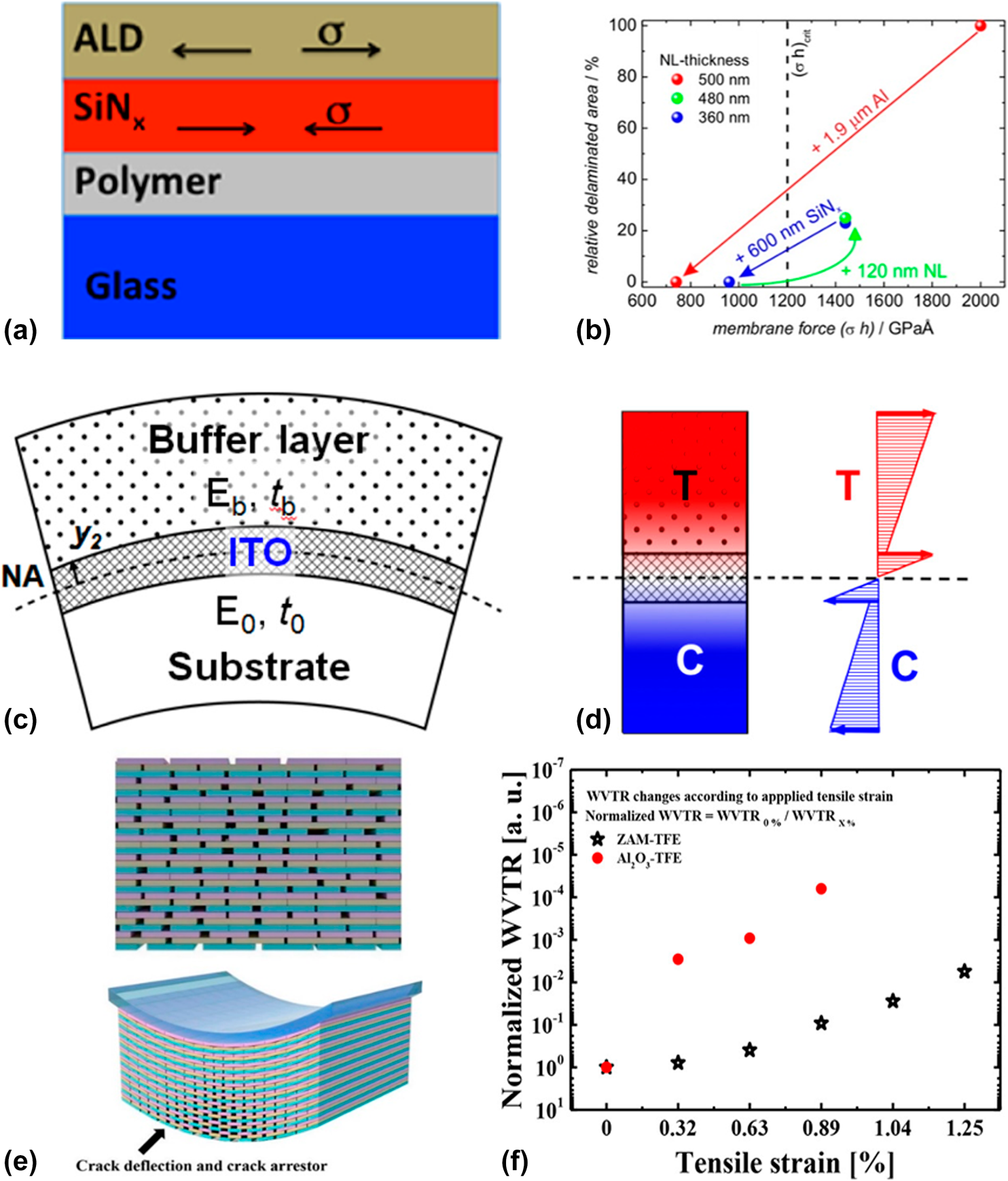
It means that the membrane force of the multilayer does not depend on the sequence of the sublayers, which has been demonstrated by the experimental data. By introducing layers with compressive stress [such as SiNx or Ag films, as shown in Fig. 5(b)] into the hybrid laminated structures [Reference Behrendt, Meyer, van de Weijer, Gahlmann, Heiderhoff and Riedl83], the membrane force can decrease to be below the threshold level.
The internal stress of the inorganic barrier structures can be released by combining the layers with reversal stress, but the barriers still tend to crack due to the bending fatigue when external stress is applied. The applied strain of the barriers under flexural deformation is proportional to the distance from the NA:
 $$\varepsilon = \left( {{{Z - {Z_{{\rm{NA}}}}} \over R}} \right)\quad ,$$
where the Z NA denotes the neutral position and R means the bending radius. Besides, the thermal mismatch strain, humidity strain, etc., can be ignored when compared with the strain induced by bending. Thus, by shifting the neutral surface toward the barrier structure can reduce the external stress effectively. As for the simplified multilayer structure model, the NA position can be deduced as below:
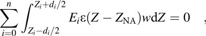 $$\sum\limits_{i = 0}^n {\int_{{{{Z_i} - {d_i}} / 2}}^{{{{Z_i} + {d_i}} / 2}} {{E_i}\varepsilon \left( {Z - {Z_{{\rm{NA}}}}} \right)w{\rm{d}}Z = 0} } \quad ,$$
where Z i, E i, d i, and w denote the location of the centroid, the elastic modulus, the thickness and cross-sectional width of the ith layer, respectively, and the 0th material means the bottom device. As for the individual layers, the location of the centroid (Z i) of them will be utilized to simplify the calculation. Combing the Eqs. (3) and (4), the location of the NA position was deduced as below:
 $${Z_{{\rm{NA}}}} = {{\sum\limits_{i = 0}^n {{Z_i}{E_i}{d_i}} } \over {\sum\limits_{i = 0}^n {{E_i}{d_i}} }}\quad .$$
In the preparation of the flexible OLED devices, d 0 ≫ d i(i ≠ 0), which revealed that the substrate thickness affects the applied strain on the barriers a lot. The theory was firstly applied in the design of the flexible OLEDs [as shown in Figs. 5(c) and 5(d)] [Reference Lee, Kwon, Yoon, Cho, You, Kang, Choi and Hwang84]; Hwang et al. revealed that the stress of the ITO could be released significantly by adding a 250-μm-thick polyimide (PI) buffer layer, whose thickness is nearly equivalent to that of the PES substrate (200 μm), and the strain decreased significantly when compared with that of OLED without buffer layer. Kim et al. added an epoxy top coating to shift the NA toward the encapsulation layer, and the barrier performance of the SiO2/Al2O3 laminates maintained unchanged under the 6.4 mm radius of curvature [Reference Kim and Graham85] (Table III, line 10). Similarly, Xu et al. added an organic protective layer [CYOTP, polydimethylsiloxane (PDMS), and SU-8] to the Al2O3/MgO laminates prepared by ALD, in which the hydrophobic organic layer can protect the inorganic barrier from being corroded in the harsh environment and improve the flexibility [Reference Wang, Ruan, Li, Zou, Hong, Peng and Xu86] (Table III, lines 11–13). In addition, inspired by the microcrack toughening effect of the nacre structure, Jeong et al. reported the ZnO/Al2O3/MgO (ZAM) laminated barrier structure for the flexible displays [Reference Kwon, Jeon, Choi, Park, Kim and Choi60]. The ZAM film was formed with intentional voids and defects through the formation of a quasi-perfect sublayer, which is shown in Fig. 5(e). It was reported that the defect densities of ALD deposited films decreased linearly with thickness until reaching the critical thickness [Reference Klumbies, Schmidt, Hähnel, Singh, Schroeder, Richter, Mikolajick, Hoßbach, Albert, Bartha, Leo and Müller-Meskamp87]. Based on that, the cycles were controlled for forming the first ultrathin films, maximizing the defect densities in sublayers before the formation of a perfect film with full coverage. The deposition process was optimized as cyclic ratio of 20/12/10 for the ZAM laminated structure, promoting the amorphous and layer-by-layer structure (Table III, line 15). The barrier property and mechanical stability of the ZAM/organic hybrid structure under different strains improved significantly in comparison with an Al2O3/organic multi-barrier in the severe environment of 85 °C/90% RH [Reference Kwon, Jeon, Choi, Kim and Choi88].
Summary of the barrier properties of hybrid laminated structures.
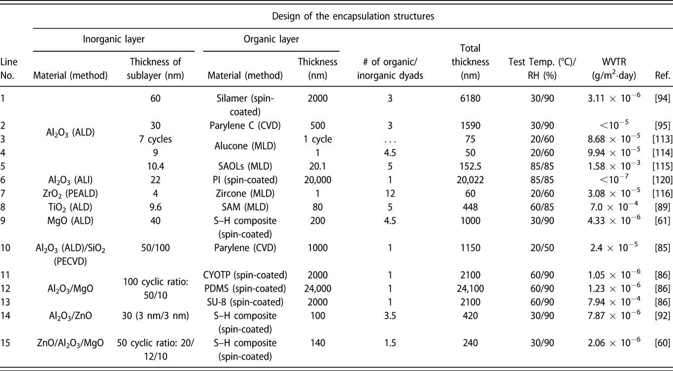
The particle generated during the fabrication of OLEDs or barrier structures also leads to the cracking, and it has been revealed that ALD is not effective for conformal coating on large particles and defects by Keuning et al. [Reference Keuning, van de Weijer, Lifka, Kessels and Creatore18]. The polymers with flexibility and the very low elastic modulus and hardness are possible to address through the presence of particle contamination [Reference Keuning, van de Weijer, Lifka, Kessels and Creatore18, Reference Seo, Jung, Lim, Chae and Cho89]. Therefore, the inorganic/organic laminated structures are considered [Reference Ylivaara, Liu, Kilpi, Lyytinen, Schneider, Laitinen, Julin, Ali, Sintonen, Berdova, Haimi, Sajavaara, Ronkainen, Lipsanen, Koskinen, Hannula and Puurunen24], in which the barrier performance is dominated by the inorganic layers, and inorganic layers can be decoupled from the inorganic layer underneath by inserting the organic layers [Reference van de Weijer, Bouten, Unnikrishnan, Akkerman, Michels and van Mol90]. Meanwhile, the organic layers can release the internal stress of the encapsulation structures. Choi and colleagues investigated the MgO/S–H composite laminates [Reference Kim, Han, Kim, Choi, Im and Bae61] and revealed that the silicon particles embedded in the organic layers can extend the diffusion path effectively, resulting in the superior barrier performance equivalent to the glass lids (Table III, line 9). However, when immersed in water, the S–H composite could not protect the inorganic layers from being corroded effectively [Reference van de Weijer, Bouten, Unnikrishnan, Akkerman, Michels and van Mol90]. Besides, Park and colleagues reported that the UV-cured procedure for S–H composite in the OLEDs [Reference Weaver, Michalski, Rajan, Rothman, Silvernail, Brown, Burrows, Graff, Gross, Martin, Hall, Mast, Bonham, Bennett and Zumhoff91, Reference Jeong, Kwon, Han, Im, Bae and Choi92, Reference Yun, Jang, Nam, Kim, Seo and Park93] degraded the emitting layer. Thus, the introduction of thermally curable organic layers at low temperature is preferred in the fabrication of inorganic/organic alternating stacks, and the use of an ALD chamber with a vacuum below 10 Pa can lower the boiling point, enabling the organic layers to be cured at a relatively lower temperature. The silamer [Reference Kwon, Jeong, Jeon, Kim, Lee and Choi94] and parylene C [Reference Wu, Fei, Wei, Chen, Nie, Zhang, Su and Cui95] were also utilized in the inorganic/organic laminates, which showed a significant surface planarization effect. The water–corrosion-resistant polymers with randomly formed three-dimensional inner structures can protect the inorganic layers effectively due to the long tortuous diffusion path. Meanwhile, no significant increase in WVTR values was found after the bending tests due to the excellent mechanical stability of the inorganic/organic laminates.
In the inorganic/organic laminated structures discussed above, pinholes are frequently found in the organic layers fabricated by the sol–gel methods [Reference Semaltianos96]. Besides, the conformality and compositional uniformity at very small thickness are hard to guarantee [Reference Liang, Kohsaka, Matsuo, Li and Ueda97]. The dry processes for depositing polymeric thin films have been proposed to overcome the problems aforementioned, such as CVD [Reference Alf, Asatekin, Barr, Baxamusa, Chelawat, Ozaydin-Ince, Petruczok, Sreenivasan, Tenhaeff, Trujillo, Vaddiraju, Xu and Gleason98]. However, the free radicals utilized in CVD method may cause the loss of the precursors’ functionalities [Reference Zhou and Bent99], and the film properties like molecular orientation are hard to control. The method called molecular layer deposition (MLD) was proposed to fabricate the ultrathin organic films with precise thickness control, excellent uniformity, and conformity. The principle of MLD is similar to that of ALD, in which different precursors are injected into the chamber subsequently, which are separated with the purge processes, and it has been successfully applied to the fabrication of polyamide [Reference Adamczyk, Dameron and George100], polyimide [Reference Putkonen, Harjuoja, Sajavaara and Niinistö101], polyuria [Reference Loscutoff, Zhou, Clendenning and Bent102], etc. [Reference Yoshimura, Ito, Nakayama and Matsumoto103]. Besides, when replacing the inorganic oxidant reactants (like H2O and O3) with the organic ones (such as diols and carboxylic acids) in the ALD processes, the hybrid films with organic backbones and metal elements can be obtained. It has been reported to prepare alumina alkoxides (alucone) [Reference Dameron, Seghete, Burton, Davidson, Cavanagh, Bertrand and George104], zinc alkoxides (zincone) [Reference Peng, Gong, VanGundy and Parsons105, Reference Cho, Han, Kim and Sung106], titanium alkoxides (titanicone) [Reference Abdulagatov, Hall, Sutherland, Lee, Cavanagh and George107], etc., which possess lower hardness and elastic modulus than the corresponding oxides (Al2O3, ZrO2, TiO2, etc.) [Reference Lee, Yoon, Anderson and George108]. However, the polymer-like hybrid films would uptake water in the ambient, leading to the erosion of the inner structure [Reference Dameron, Seghete, Burton, Davidson, Cavanagh, Bertrand and George104]. When covered with the inorganic layer, the degradation can be inhibited effectively [Reference Cho, Han, Kim and Sung106]. As discussed elsewhere, due to the thermal expansion difference of the inorganic films and the plastic substrates, the films tend to crack with increasing thickness. Following Griffith’s criterion, when the strain energy release rate (G) from the surrounding strained material exceeds the interfacial toughness (Γi), the crack will continue to propagate [Reference Waters and Volinsky109]. Here, the amount of stored elastic energy per unit area in a stressed thin film is:
 $$G \equals Z{{\sigma _{\rm{r}}^2h} \over E}\quad ,$$
where Z is a geometric constant, which ranges from 0.5 to 2.0 and σr and h denote the residual stress and thickness of the deposited films, respectively. E is the film’s biaxial elastic modulus. With the increase in film thickness h, the residual stress increases gradually, especially when the high coefficient of thermal expansion (CTE) mismatch exists between the film and substrate. Both the increasing thickness and residual stress contribute to the increase in the stress release rate, and the crack can be observed due to the release of large amounts of energy. As shown in Figs. 6(a) and 6(b), George and colleagues reported that the insertion of the MLD interlayer could release the stress in the inorganic layers, and it was assumed that the “spring-like” organic interlayer with minimal cross-linking between the polymer chains could lower the compressive stress applied to the inorganic films [Reference Jen, George, McLean and Carcia26], leading to the decrease in the crack probability [Reference Park, Oh, Kim, Jung, Choi and Park110, Reference Miller, Foster, Jen, Bertrand, Seghete, Yoon, Lee, George and Dunn111, Reference Miller, Foster, Zhang, Jen, Bertrand, Lu, Seghete, O’Patchen, Yang, Lee, George and Dunn112]. Duan and colleagues demonstrated the improved barrier property of the alucone/Al2O3 nanolaminates compared with that of Al2O3 single layer with the same thickness, which was due to the extended permeation path [Reference Feng-Bo, Yu, Yong-Qiang, Ping, Ya-Hui, Xiao, Dan and Kai-wen113] (Table III, line 3), and the flexibility was also enhanced [Reference Xiao, Hui, Zheng, Yu, Yong Qiang, Ping, Xiang and Yi114, Reference Yoon, Kim, Han, Kim, Lee, Shrestha, Song and Sung115, Reference Chen, Wang, Wang, Chen, Liu, Zhao, Zhao and Duan116].
(a) Schematic depicting the “spring-like” nature of the alucone interlayer between the Al2O3 ALD film and the Teflon FEP substrate; (b) compressive stress on 21 nm ALD-based Al2O3 versus alucone interlayer thickness on Teflon fluorinated ethylene propylene (FEP) substrates with thickness of 50 and 125 μm; (c) schematic illustration of fabrication of polymer hybrid thin layer via ALI method; (d) Ca dot corrosion tests for PI films after they were subjected to 10,000 bending cycles.
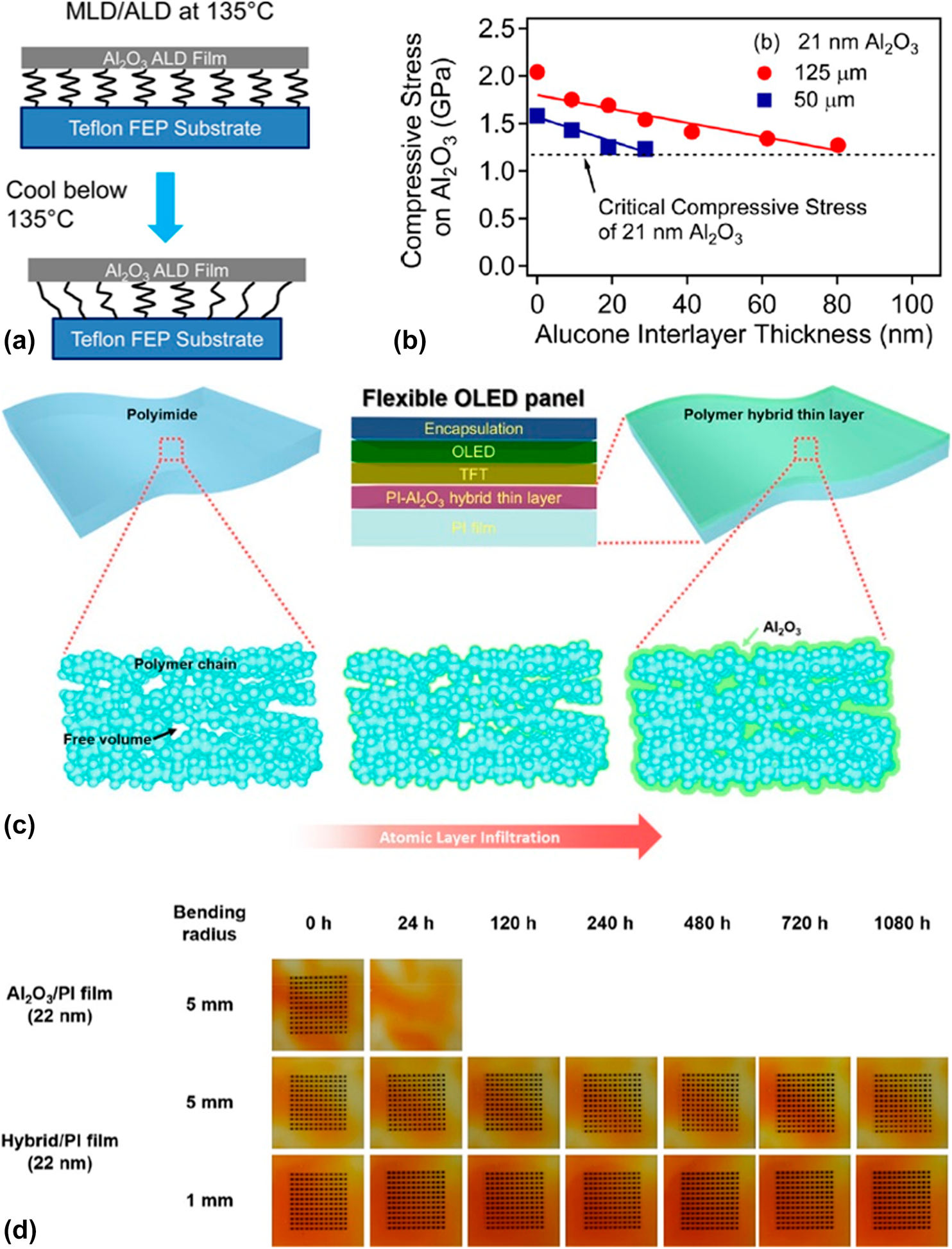
Although the polymer substrates (such as PET and PEN) perform poor barrier property, their excellent flexibility attracts great interests from the researchers. Besides, the polymer films are easy to achieve high-throughput and low-cost fabrication with sol–gel methods. Nowadays, ALD method has been utilized to tune the mechanical and barrier properties of the polymer substrates widely [Reference Parsons, Atanasov, Dandley, Devine, Gong, Jur, Lee, Oldham, Peng, Spagnola and Williams117, Reference Tsai, Wang, Lu, Tseng, Lu, Huang and Yeh118]. To be exact, the growth behavior on the polymer substrates is strongly dependent on the chemical bonds (such as –OH, –C=O–, and –NH2) and process parameters (temperature, purge time, etc.) [Reference Wilson, Grubbs and George119], which have been demonstrated by the quartz crystal microbalance and in situ FTIR investigations. The TMA molecules would diffuse into the sublayer and react with the groups on the surfaces, and the diffusion depth can be controlled to a certain extent by adjusting the process parameters. As shown in Fig. 6(c), Lee et al. reported a gas-proof polymer hybrid thin layer prepared via the atomic layer infiltration [Reference Lee, Yoon, Jung, Yoon, Kim, Kim, Song, Park and Sung120]. Compared with the ALD method, the precursors would not be purged out of the reaction chamber as soon as possible after the pulse, and the chamber was completely closed for a certain period for the precursors to diffuse into the polymers. After several tens of cycles, the voids in the substrates could be filled completely, which was confirmed by the energy-dispersive X-ray spectroscopy, and the barrier property reached below 10−7 g/m2·day while maintaining excellent flexibility (Table III, line 6), which is shown in Fig. 6(d). The barrier properties of the different hybrid laminated structures are listed in Table III.
Thermal management layers
Except for the degradation caused by the moisture erosion in the ambient, the flexible OLEDs based on the plastic substrates with low thermal conductivity face serious performance degradation if no additional heat sink system conducting the heat out of the device is contained [Reference Kwak, Cho and Kim121]. Park et al. reported that the efficiency and lifetime were improved by inserting a metal sheet [Reference Park, Shin and Park122], but the rough surfaces and additional physical pressure would damage the OLED devices. Therefore, an ultrathin heat conducting film with excellent flexibility, ductility, and transparency is needed for the encapsulation for flexible OLEDs.
Among the various materials, graphene and silver possess the best heat conductivity, but the former one needs to be prepared with the CVD method, in which high temperature and catalysts are needed. Due to the simplicity of preparation process, Ag layer is more commonly adopted. Kwon et al. reported a dielectric–organic metal encapsulation structure to guarantee the reliability of flexible OLEDs [Reference Kwon, Choi, Jeon, Kim, Chang and Choi123], which is shown in Fig. 7(a). The thickness optimization of Ag layer is crucial for the device performance, in which a discontinuous Ag layer leads to the nonuniform heat transfer, whereas a thick layer leads to the low transparency. The kick point where the Ag film turned from discontinuous to continuous was shown photographically by the AFM or SEM, and it could also be deduced by the sharp decrease in the sheet resistance [Reference Kwon, Jeon and Choi57]. The overall structure was optimized via optical simulation via Matlab software, and it was found that the transmittance of Al2O3/Ag/Al2O3 structure was 33% higher than that of the Al2O3/Ag structure due to the anti-reflection effect [Reference Kwon, Choi, Jeon, Kim, Chang and Choi123]. Finally, the nanocomposite organic layer was inserted to improve the flexibility further, and the Al2O3/Ag/Al2O3/S–H nanocomposite/Al2O3 multilayer structure was obtained. As shown in Fig. 7(c), the infrared camera was used to observe the real-time temperature profiles of the OLEDs operated at the certain input power, and it was demonstrated that the insertion of the Ag layer in the multilayer structure helped conduct the heat out of the devices effectively, which prolonged the lifetime of the OLEDs. Besides, the excellent flexibility and barrier property of the dielectric–organic metal encapsulation structures were demonstrated before and after the bending tests.
(a) Schematic of Al2O3/Ag/Al2O3/S–H nanocomposite/Al2O3 barrier structure; (b) sheet resistance of MAZO/Ag and MAM structures in relation to Ag thickness; (c) real-time temperature profiles of FOLEDs at an input power of 80 mW over time; (d) Al2O3/graphene composite barrier layer; and (e) electrical Ca tests of different barrier structures.
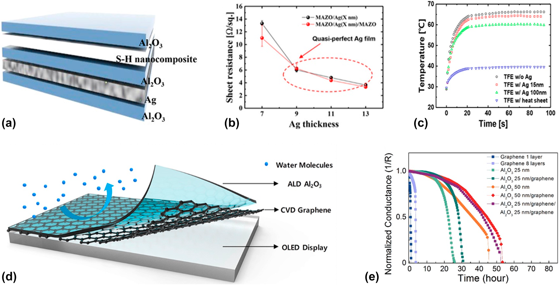
The graphene possesses better heat conductivity and barrier property than those of Ag layer. Theoretically, the lattice constant of graphene is 2.47 Å, which is smaller than the size of H2O molecular (around 4.0 Å). It means that the perfect graphene layer can block the permeation of moisture effectively. To apply the artificial graphene films fabricated via CVD method to flexible electronics, Ruoff and colleagues transferred them to target substrate by an optimized process with the assistance of PMMA [Reference Han, Lee, Choi, Woo, Bae, Hong, Ahn and Lee124, Reference Li, Zhu, Cai, Borysiak, Han, Chen, Piner, Colombo and Ruoff125]. As a good conductor, the insulator is needed to be inserted between the OLEDs and graphene, such as PDMS and PMMA. However, Karnik and colleagues revealed that the CVD-grown single-layer graphene had various defects, such as pinholes and cracks [Reference Boutilier, Sun, O’Hern, Au, Hadjiconstantinou and Karnik126]. Seo et al. prepared the multi-stacked graphene films to form a defect-sealed membrane, and it was found that the permeation rate decreased with the increase in the graphene layers [Reference Seo, Park, Kim, Kwon, Jeong and Lee127], but which was still far from the requirements of OLEDs. As shown in Figs. 7(d) and 7(e), Nam et al. used the ALD-based Al2O3 to passivate the defects of the graphene films [Reference Nam, Park, Lee, Oh, Ahn, Cho, Kim and Lee128] and the barrier property improved significantly.
ALD reactors and processes for TFE
Notably, the ALD precursors are most aggressively reactive, which may lead to the degradation of the chemically active OLED materials. Thus, the chemical compatibility of these as-mentioned ALD techniques with current OLED materials need to be discussed. Singh et al. investigated how the different oxidant precursors (H2O and O3) affected the luminous performance and lifetime of OLEDs. In the experimental procedures, the pulse and purge duration for TMA was fixed at 0.3 s pulse and 0.75 s purge, and the pulse duration for the oxidant precursor ranged from 1 to 45 s, and the purge duration maintained half of the pulse time [Reference Singh, Klumbies, Schröder, Müller-Meskamp, Geidel, Martin, Hoßbach, Albert, Leo and Mikolajick129]. Besides, the deposition temperature was set as 50 °C. The results indicated that the O3-based process seemed to be more compatible with the OLEDs than the H2O-based process [Reference Singh, Nehm, Müller-Meskamp, Hoßbach, Albert, Schroeder, Leo and Mikolajick130]. As reported elsewhere, the activation energy for Alq3 hydrolysis (the emitting layer in OLEDs) is 35% lower than that of the pure Alq3, and the hydrolyzed Alq3 would lead to the nonemissive area [Reference Knox, Halls, Hratchian and Schlegel131]. Thus, the ozone-based Al2O3 was deposited on the OLED surfaces directly, which can block the H2O diffusion in the later processes of H2O-based Al2O3 films, and the blocking effect improves with the increasing O3-based Al2O3 film thickness. To avoid the direct contact with the precursors, Park et al. inserted a 3-μm-thick organic buffer layer between OLED and Al2O3 barrier layer, and the pulse time of the precursors was optimized at the same time [Reference Park, Oh, Hwang, Lee, Yang and Chu62]. It can be found that several dark spots formed in the emitting image when the H2O pulse time was set as 1.43 s, but no black spot was found when the pulse time was reduced to 0.5 s even without the buffer layer. In particular, to improve the performance of the OLED devices, the stacks consisting of materials with high and low refractive indexes would be deposited on the top of the devices, which serve as the optical functional layer to improve the light output. Thus, the chemically active OLED materials will not be exposed to the precursors directly, leading to the enhanced stability and reliability.
Various commercial ALD reactors have been reported for the continuous industrial production. Picosun (Espoo, Finland) has integrated the roll-to-roll module in the reaction chamber, which can be used for the flexible substrates with the width of 70 mm. Similarly, Beneq (Espoo, Finland) has also published its roll-to-roll ALD system, and the web speed of which can reach 10 m/min. The Firebird ALD equipment invented by Veeco Company (Waltham, Massachusetts) can be utilized to fabricate the barrier layers and optoelectronics [Reference Takeuchi, Ezoe, Ishikawa, Numazawa, Terada, Ishi, Fujitani, Sowa, Ohashi and Mitsuda132], and the substrates width can reach above 300 mm. It is noted that the Infinity TM500 invented by Encapsulix (Aix-en-Provence, France) can be applied to the encapsulation of displays with width reaching G5.5 (1300 × 1500 mm2), and the WVTR of 25 nm Al2O3 film reached ∼5 × 10⁻⁴ g/m2·day [Reference Maindron, Simon, Viasnoff and Lafond133]. To further improve the deposition rate, more and more deposition chambers or units are integrated to improve the efficiency, and the related equipment has been reported by ASM International (Almere, Netherlands) [Reference Gschwandtner134], Eugene Technology (Yongin-si, Korea), and Leadmirco (Wuxi, China), which mainly serve for the semiconductor and solar cells.
However, with the continuous expansion of the panel size, the vacuum chamber of ALD reactors can no longer meet the requirements of large area and high throughput. Moreover, a long purge time is needed to clean the excessive precursor and by-product in the low-temperature process. Kwon et al. reported that the Al2O3 monolayer with the thickness of ∼60 nm performed the best barrier property, which could strike a balance between pinhole density and internal stress [Reference Kwon, Jeong, Jeon, Kim, Lee and Choi94]. However, it is calculated that more than 4 h would be spent, which is far from the efficiency of the PE-CVD method. The spatial atomic layer deposition (SALD) is thought to be a potential method to solve this issue [Reference Suntola and Antson135, Reference Suntola, Pakkala and Lindfors136]. Compared with the thermal ALD, the precursors will be injected into the reaction chamber continuously, and different precursors and the ambient will be separated by the inserted physical gas barriers. The substrate moves underneath the injectors cyclically, and the thickness can be controlled precisely by adjusting the cycle numbers. Choi et al. developed the high-throughput SALD system for the TFE of OLEDs, and it was applied to the 2G glass substrate (370 × 470 mm2) with the deposition rate of 7 nm/min. The barrier property of the PEN substrates coated with 100-nm-thick nanolaminates improved from 1.8 × 10⁻³ to 6.9 × 10⁻⁵ g/m2·day [Reference Choi, Shin, Choi, Choi, Kim, Kim, Kim, Park, Chung, Jeon and Oh137]. Franke et al. developed their SALD system integrated with a microwave plasma source, and the WVTR value of 50 nm Al2O3 could reach ∼10−6 g/m2·day [Reference Franke, Baumkötter, Monka, Raabe, Caspary, Johannes, Kowalsky, Beck, Pucci and Gargouri56]. Due to the simplicity of the linear track one, we also developed the modular injector integrated SALD apparatus, and the deposition rate reached 100 nm/min with the nonuniformity around 2% [Reference Wang, Li, Lin, Shan and Chen138]. Besides, George and colleagues developed a modular rotating cylinder SALD reactor, in which the inner cylinder rotated with the flexible substrate and passed underneath the various spatially separated slits in the outer cylinder [Reference Sharma, Hall and George139]. Poodt et al. developed the rotary SALD equipment and applied it to the passivation of silicon solar cells, and the drastic increase in the solar cell efficiency was found [Reference Poodt, Lankhorst, Roozeboom, Spee, Maas and Vermeer140]. Similar commercial equipment such as the InPassion ALD invented by SoLayTec has also been reported [Reference Souren, Gay, Dielissen and Görtzen141], in which more than 4 deposition units are integrated, resulting in the production efficiency of 4500 wafers per hour. Meanwhile, ASTRal and TNO had developed the roll-to-roll SALD equipment, which can be applied in the encapsulation of flexible electronics with the width more than 300 mm [Reference Poodt, Cameron, Dickey, George, Kuznetsov, Parsons, Roozeboom, Sundaram and Vermeer142, Reference Illiberi, Roozeboom and Poodt143, Reference Levy, Freeman, Nelson, Cowdery-Corvan and Irving144, Reference Poodt, Knaapen, Illiberi, Roozeboom and van Asten145].
Except for the limitation of substrate size and low deposition rate, the demand of low-temperature process for polymer substrates requires that only the precursors with high reactivity (such as TMA, DEZ, and TiCl4) can be adopted. However, the oxides will be deposited on the chamber walls and masks at the same time, which are hard to be removed, leading to the particle contamination of the barrier structures after a long period. One of the solutions to solve this problem is to synthesize the new precursors for the oxides such as SiO2, which ought to possess high reactivity and adequate saturated vapor pressure, and the by-product is easy to be eliminated. Besides, the SiO2 film deposited on the chamber walls and masks are easy to be removed by introducing the corrosive gas, which can promote the cleanliness of the chamber. Another way is to develop the plasma-enhanced atomic layer deposition (PEALD) method, in which the oxidant (such as O2, N2) can be activated by the electric fields, and the process temperature can be lowered to the room temperature. It has been successfully applied in the preparation of AlN [Reference Ozgit, Donmez, Alevli and Biyikli146, Reference Bosund, Sajavaara, Laitinen, Huhtio, Putkonen, Airaksinen and Lipsanen147] and SiO2 [Reference Gebhard, Mai, Banko, Mitschker, Hoppe, Jaritz, Kirchheim, Zekorn, de los Arcos, Grochla, Dahlmann, Grundmeier, Awakowicz, Ludwig and Devi148], and the SALD method can also be integrated to increase the deposition rate [Reference Yong-Qiang, Yu, Ya-Hui, Xiao, Ping, Dan, Feng-Bo and Kai-wen49]. Compared with the thermal ALD, denser films can be obtained via PEALD, and the excellent barrier property of the monolayer or laminated encapsulation structures [Reference Kim, Kim, Park, Jeong, Kim, Chung, Kim and Park59, Reference Lee, Choi, Shin, Park, Ham, Jung and Jeon77, Reference Chen, Wang, Wang, Chen, Liu, Zhao, Zhao and Duan116] has been demonstrated.
Summary and outlook
OLEDs are attractive for flexible displays; yet, the reliability is of great challenge to overcome pinholes and crystallization, cracks, and overheated through barrier layers. The ALD-based TFE has emerged as a powerful method to solve the existing issues. The monolayer and composite structures fabricated via ALD can decouple the pinhole defects, and the nanolaminates possess superior water–corrosion-resistant property and inhibit the crystallization. Moreover, hybrid laminated structures can reduce internal stress and improve the flexibility, and an additional heat sink system is embedded to transfer the heat out to avoid the thermal aging. Besides, the SALD and PEALD methods have been proposed to improve the deposition rate and to extend the range of the precursors that can be utilized.
Nevertheless, there are some remaining challenges to be addressed toward further flexibility and potential stretchable displays. With the thickness continuing to go down, the encapsulation structures have to be further optimized with consideration of optical emittance, barrier resistance, and mechanical robustness. A database containing different inorganic or organic materials needs to be built based on the different experimental processes, which covers the parameters of mechanical, optical, thermal, and barrier properties corresponding to different processes. The interfaces between multilayer hybrid films need more accurate theoretical simulations with interface consideration. Moreover, the barrier structures are expected to replace the original capping layer of the OLEDs, leading to the simplified device structures, and the moistures can be blocked effectively.
Another obstacle currently is how to fabricate large-scale organic layer with accurate thickness control and good throughput, as organic layers play an important role in the design of the ultra-flexible barriers. Inspired by the SALD methods, the oxidant precursor can be replaced by the organic materials, and the spatial molecular layer deposition (SMLD) will be achieved. However, the isolation between different precursors in the SMLD will be more complex due to high viscosity of organic precursors. A more reliable method to fabricate the organic layers is ink-jet printing, in which lots of nozzles can be integrated to satisfy the requirement of large-area substrates. Besides, the future stretchable electronics will require TFE as well, and the organic–inorganic hybrid layers with excellent tensile properties need to be developed.
Another issue ALD currently faces urgently is the self-clean. Current ALD components have strongly relied on Al2O3 and other hard-to-etch materials. It is important to have SiOx investigated and be able to grow with low temperature on large scale. The ALD precursor development also needs to be addressed. On the other hand, in the preparation process of the barrier structures, the masks are necessary to protect the electrodes from being covered by the dielectric films. Meanwhile, they also play an important role in the fabrication of the patterned structures for the OLEDs, especially for the MicroLED. Therefore, the frequent cleaning of masks or adopting the thin film deposition processes, which can realize the in situ self-cleaning, is necessary to avoid the particle contamination. Besides, how to promote the high accuracy of linewidth resolution on the edge area is of great importance. The area-selective ALD is expected to streamline the process flow and solve the broken inorganic layers with small folding radius, and TFEs only deposit where they are needed.
The design of the encapsulation structures of the flexible OLEDs is a systematic and complex project, and the ALD method will play a more important role in the future due to its unique assets.
Acknowledgments
This work was supported by the National Natural Science Foundation of China (51835005, 51575217, and 51702106). The authors acknowledge the Flexible Electronics Research Center of Huazhong University of Science and Technology. The authors also thank Yinghao Zhang and Yuan Lin from Huazhong University of Science and Technology and Dr. Jing Huang from Wuhan China Star Optoelectronics Technology Co., Ltd., for the instructive discussions.