Introduction
Dynamic random-access memory (DRAM) device is the most important device among semiconductor memory devices because of its wide range of applications in the IT industry, which include PCs, servers, and mobile phones. The necessity and importance of DRAM have increased because of the tremendous amount of data to be processed in the big data industry (which is one of the most important industries in the fourth industrial revolution) and the increased demand for various electronic devices [Reference Hwang1]. In this regard, the market for DRAM has increased dramatically in the past decades, and this increase has reached unprecedented levels in recent years. As a consequence, research about DRAM devices has attracted a lot of attention from academia and industry. Because the capacitor primarily governs operational characteristics of the DRAM device, most research on DRAM has focused on implementing performance enhancements in the DRAM capacitor. The DRAM capacitor, which consists of a metal–insulator–metal (MIM) structure, requires low leakage current density and high capacitance density for robust operations (e.g., read, write, and refresh). In the early stages of development, decreasing the dielectric thickness or increasing the capacitance area by changing the structure of the MIM capacitor could be used to meet the specifications of DRAM capacitors [Reference Kotecki2, Reference Scott3]. However, using dielectric materials with a high dielectric constant (k) was inevitable in the era of design rules beyond sub-100 nm [Reference Kim and Popovici4, Reference Wilk, Wallace and Anthony5]. High-k materials allow the same capacitance density as a thicker physical thickness, which can effectively suppress the leakage current through tunneling mechanisms. However, additional problems have emerged when using high-k materials. First, other leakage conduction mechanisms offset the leakage current reduction effect observed when using the high-k dielectric [Reference Jegert, Kersch, Weinreich and Lugli6, Reference Robertson and Wallace7, Reference Zhu, Low, Lee, Wang, Farmer, Kong, Xia and Avouris8, Reference Baniecki, Shioga, Kurihara and Kamehara9]. These mechanisms originate from large defect densities or narrow band gaps and include trap-assisted tunneling (TAT), Poole–Frenkel (P–F) emission, Schottky emission, or Fowler–Nordheim (F–N) tunneling. Moreover, further scaling beyond sub-10 nm causes new limitations in the physical thickness of dielectrics when designing MIM structures as thin as possible [Reference Kim and Popovici4]. Ironically, the high-k material was originally introduced to realize a higher physical thickness [Reference Robertson10]. As a consequence, the requirements of high-k materials for next-generation DRAM capacitor applications include both conventional goals (e.g., low leakage current and high capacitance density) and the thinnest possible physical thickness.
Leakage current in the metal–insulator–metal structure with high-k materials
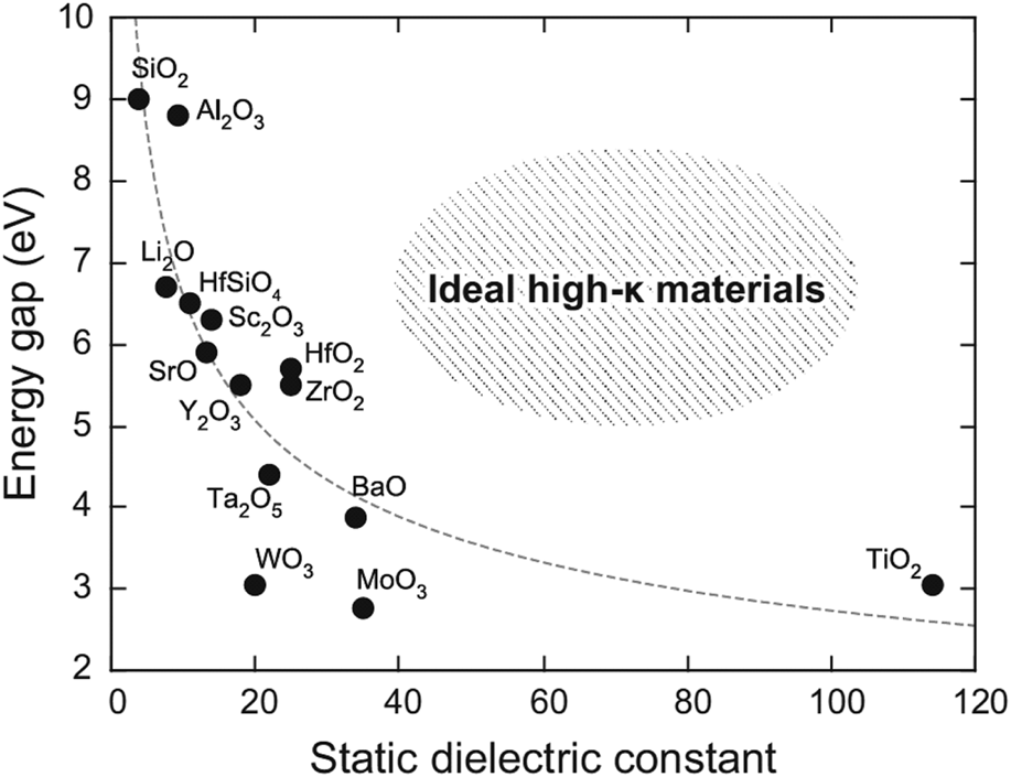
Leakage current through a dielectric layer in MIM capacitors results in severe degradation in DRAM device operation because data in a DRAM unit cell is stored by charging carriers in the MIM capacitor. In this regard, leakage current reduction is a key issue in DRAM device investigations, and this is the reason why high-k materials have been introduced as an insulator in the MIM capacitor. However, MIM capacitors with high-k materials have suffered from leakage currents because of the weak dielectric strength of high-k materials (Fig. 1) [Reference Yim, Yong, Lee, Lee, Nahm, Yoo, Lee, Hwang and Han11, Reference Khan, Kim, Taniguchi, Ebina, Sasaki and Osada12]. Whereas direct tunneling should be considered as an only carrier conduction mechanism in the case of using SiO2, several such mechanisms could contribute to leakage current when using high-k materials, resulting in weak dielectric strength of high-k materials. Figure 2 depicts the carrier conduction mechanisms available in ZrO2 as an example of high-k materials [Reference Jegert, Kersch, Weinreich and Lugli6]. As shown in Fig. 2, the carrier conduction mechanisms are related to defects (e.g., TAT and P–F emission) or low conduction band offsets (CBOs) (e.g., Schottky emission and F–N tunneling). In this regard, these mechanisms can be classified into two categories: bulk-related or interface-related leakage current conduction.
Band gap versus dielectric constant of various high-k materials. [Reprinted with permission from Ref. Reference Yim, Yong, Lee, Lee, Nahm, Yoo, Lee, Hwang and Han11 under CC BY-NC-SA 4.0 license. Copyright (2015) Springer Nature.]
Various leakage current conduction mechanisms on high-k material. [Reprinted with permission from Ref. Reference Jegert, Kersch, Weinreich and Lugli6. Copyright (2010) IEEE.]

Bulk-related leakage current conduction
ZrO2 and HfO2 have been extensively studied as high-k materials for replacing classical SiO2 and SiON insulators because of their relatively high k value (>20), wide band gap (E g) of 5.5–6.0 eV, and well-established atomic layer deposition (ALD) processes [Reference Liu, Ramanathan, Longdergan, Srivastava, Lee, Seidel, Barton, Pang and Gordon13, Reference Ponraj, Attolini and Bosi14, Reference Johnson, Hultqvist and Bent15, Reference George16, Reference Leskelä and Ritala17, Reference Richter, Schenk, Schroeder and Mikolajick18, Reference Kim, Park, Kim, Cho, Jung, Lee and Hwang19, Reference Schroeder, Jakschik, Erben, Avellan, Kudelka, Kerber, Link and Kersch20]. Although ZrO2 and HfO2 share many common properties, ZrO2 has been favored for DRAM capacitor applications because it can obtain a higher k phase crystal structure, tetragonal or cubic phase, in the as-deposited state [Reference Yoo, Jeon, Lee, An, Kim and Hwang21]. The k values of HfO2 and ZrO2 depend on the crystal structure, i.e., monoclinic, and tetragonal or cubic [Reference Zhao and Vanderbilt22, Reference Zhao and Vanderbilt23]. Because tetragonal or cubic phases are thermodynamically stable at much higher temperatures (about 900 °C) at atmospheric pressure, the films deposited by ALD techniques generally have a monoclinic phase crystal structure [Reference Jung, Jang, Cho, Jeon, Kim, Lee and Hwang24, Reference Lee, Jeon, Cho, Lee, Jeong, Park and Park25, Reference Lee, Yu, Lee and Hwang26]. Transition of the monoclinic phase to metastable phases and the accompanying increase in k values are quite difficult (results related to this will be discussed in section “Dopant-mediated crystallinity enhancement”). Fortunately, ZrO2 deposited by the ALD technique exhibits a higher k phase (tetragonal) in the as-deposited state, and further crystallization into the tetragonal phase is easily demonstrated by thermal treatment [Reference Yoo, Jeon, Lee, An, Kim and Hwang21].
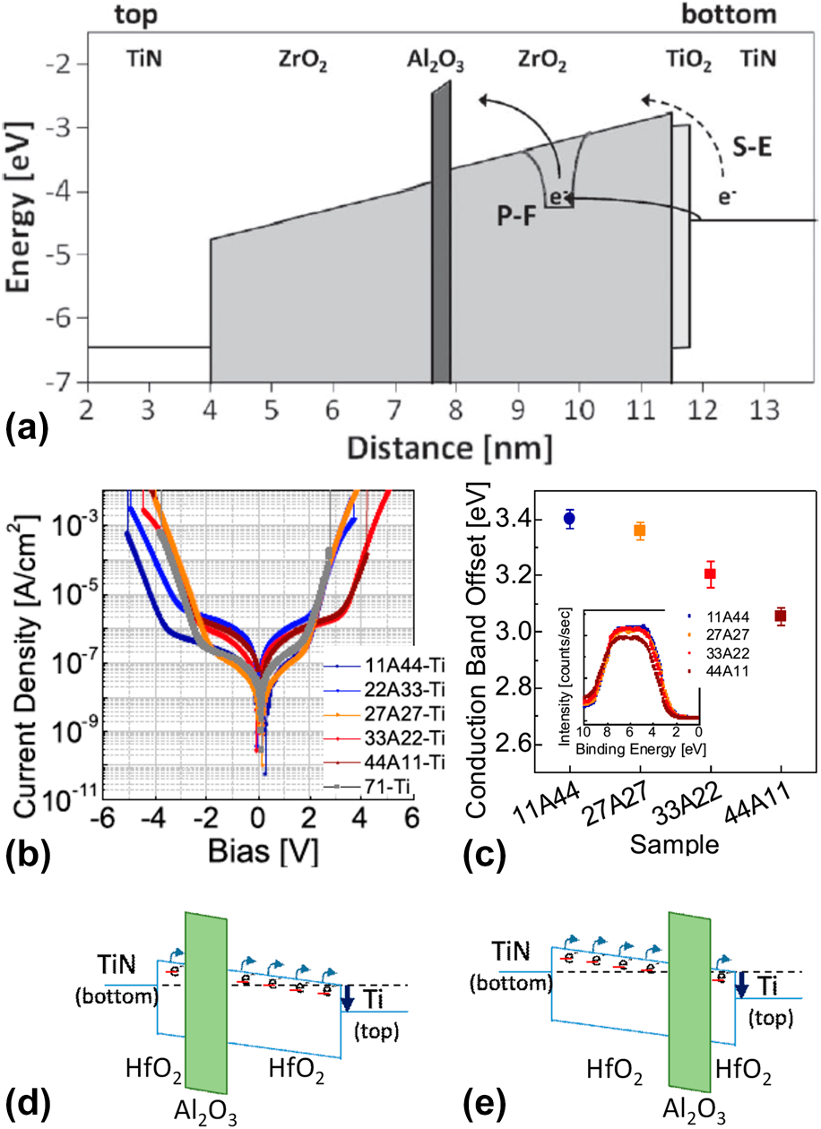
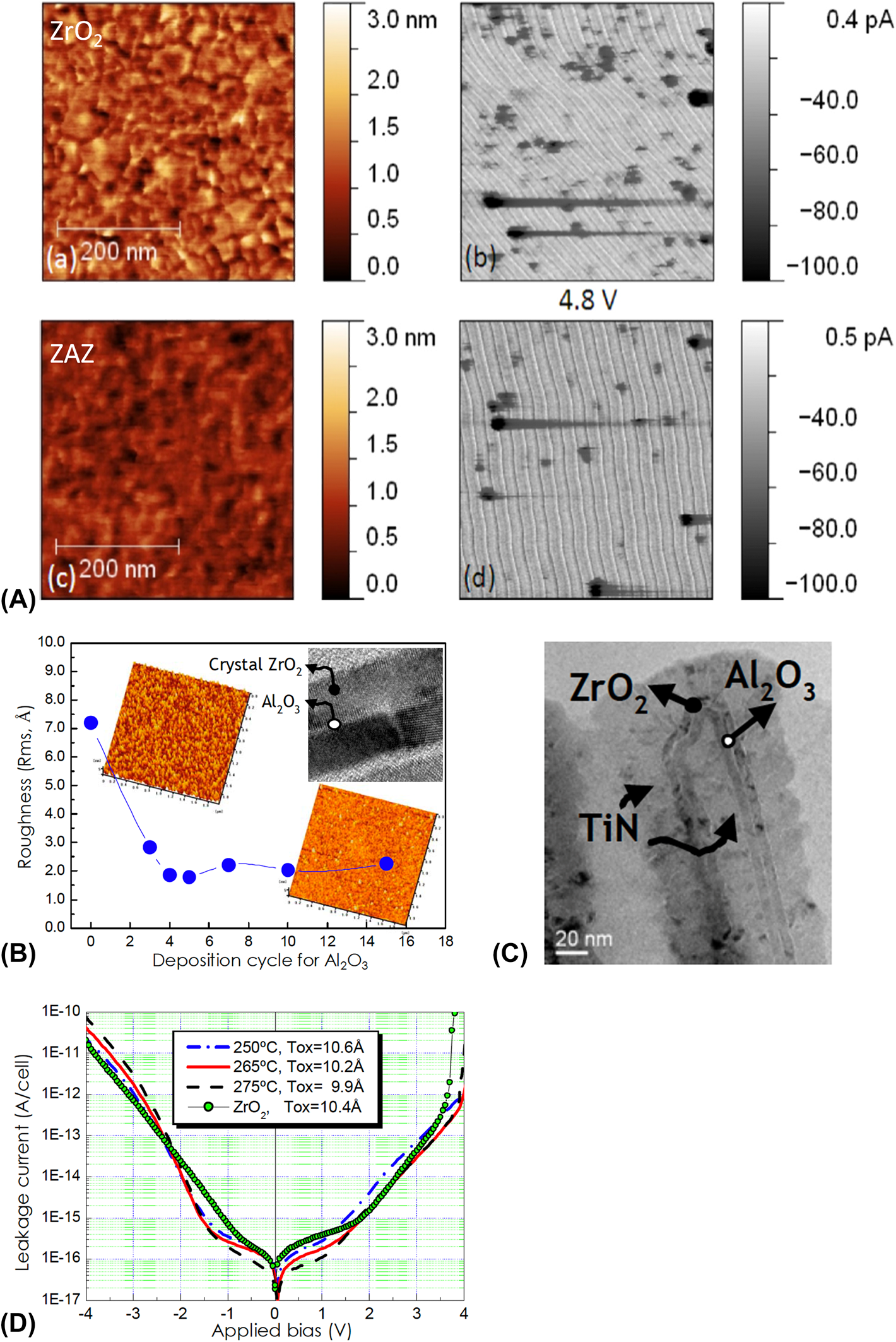
The carrier conduction mechanisms in ZrO2 have been investigated to determine an effective way of reducing leakage current (Fig. 3) [Reference Weinreich, Shariq, Seidel, Sundqvist, Paskaleva, Lemberger and Bauer27]. As shown in Fig. 3, there is a characteristic difference in the carrier conduction mechanism between ZrO2 and classical SiO2 and SiON insulators. First, current conduction by direct tunneling is not observed, and contributions from Schottky emission are not significant. These are attributed to the increased physical thickness and the relatively high E g of ZrO2. The E g values of ZrO2 are 5.5–6.0 eV, which are smaller than those of classical insulators. However, they are sufficient to create a conduction band offset (CBO) of ∼2 eV with a metal electrode (typically TiN or W) [Reference Weinreich, Shariq, Seidel, Sundqvist, Paskaleva, Lemberger and Bauer27, Reference Lee, Chang, Kim, Lim, Jeon and Seo28, Reference Lee, Chang, Choi, Kim, Lim, Jeon and Seo29, Reference Lee, Kim, McIntyre, Saraswat and Byun30, Reference Knebel, Schroeder, Zhou, Mikolajick and Krautheim31, Reference Jegert, Kersch, Weinreich and Lugli32], resulting in suppression of leakage current by Schottky emission. Consequently, carrier conduction in ZrO2 is mediated by TAT (or temperature-activated TAT, T-TAT), P–F, and F–N mechanisms in low, middle, and high electric field (E-field) regions, respectively. These mechanisms are not related to the interface between the insulator and electrode but strongly depend on the bulk properties of the insulator [Reference Jegert, Popescu, Lugli, Häufel, Weinreich and Kersch33] defects such as oxygen vacancies (V O) [Reference Jeon, Kim, An, Hwang, Gonon and Vallee34], grain boundaries [Reference Weinreich, Shariq, Seidel, Sundqvist, Paskaleva, Lemberger and Bauer27, Reference Martin, Grube, Weinreich, Müller, Weber, Schröder, Riechert and Mikolajick35], and impurities [Reference Wang36]. Grain boundaries were assumed to be the dominant carrier conduction paths. Moreover, ZrO2 thin films deposited using the ALD technique tend to have a columnar structure in the direction of film growth [Reference Kim and Hwang37, Reference Cho, Kim, Park, Lee, Park, Jang, Lee, Kim, Ki, Han and Song38, Reference Lee, Choi, Hande, Kim, Wallace, Kim, Senzaki, Shenai, Li, Rousseau and Suydam39]; this is the same as the electron drift direction in the applied E-field. Martin et al. reported the results of carrier conduction in pristine ZrO2 thin films observed by conductive atomic force microscopy (C-AFM) measurements [Reference Martin, Grube, Weinreich, Müller, Weber, Schröder, Riechert and Mikolajick35]. Here, the “trench” on the film surface, which is formed by interconnected grain boundaries, coincides with the location of carrier conduction [Fig. 4(A)], illustrating the role of the grain boundary in carrier conduction. Consequently, various ways of engineering the grain boundary structure in the film have been suggested to suppress the leakage current of ZrO2. Creating a tortuous carrier conduction path by reducing the grain size would reduce leakage current. But basic approaches such as interrupting the path by inserting an amorphous layer in the middle of the ZrO2 thin film or eliminating the grain boundary by inducing an amorphous phase in the ZrO2 itself would be more efficient for reducing leakage current. Accordingly, the ZrO2/Al2O3/ZrO2 (ZAZ) stacked structure, which was designed to reduce the path by integrating amorphous Al2O3 in the middle of ZrO2, was investigated in 2006 [Reference Cho, Kim, Park, Lee, Park, Jang, Lee, Kim, Chae, Ki, Han and Song40]. Indeed, this structure demonstrated excellent properties for DRAM devices with a 45 nm design rule. Al2O3 was inserted into the middle of the ZrO2 layer at a certain thickness (more than 0.5 nm) as a distinctive layer [TEM images in the insets of Figs. 4(B) and 4(C)], resulting in suppression of excessive grain growth during crystallization of ZrO2 as inferred from a dramatically reduced roughness of the ZAZ film [Fig. 4(B)] [Reference Kil, Song, Lee, Hong, Kim, Park, Yeom, Roh, Kwak, Sohn, Kim and Park41]. Therefore, the leakage current of an MIM capacitor with a ZAZ insulator was significantly reduced compared with that of a ZrO2 insulator in an applied bias range of −2 to +1.5 V [Fig. 4(D)] [Reference Kil, Song, Lee, Hong, Kim, Park, Yeom, Roh, Kwak, Sohn, Kim and Park41]. Indeed, a conductive atomic force microscopic (c-AFM) image of the ZAZ film [Fig. 4(A)] showed that the number of carrier conduction paths significantly decreased [Reference Martin, Grube, Weinreich, Müller, Weber, Schröder, Riechert and Mikolajick35]. Additionally, the range of applied bias with reduced leakage current was consistent with the range in which leakage current conduction of ZrO2 was governed by trap-related carrier conduction mechanisms (TAT and P–F) (Fig. 3). This implies that Al2O3 (with distinctive layer formation) can act as a carrier conduction barrier because of its relatively thick band gap of 9.0 eV [Fig. 5(a)] [Reference Knebel, Schroeder, Zhou, Mikolajick and Krautheim31]. Generally, an Al2O3 layer has been used as a barrier to carrier conduction by the CBO-related leakage currents (Schottky emission or F–N tunneling). In this regard, the location of the Al2O3 inserted to reduce leakage current tends to be at the interface between the metal electrode and the insulator. However, as shown in the ZrO2 case, inserting Al2O3 at the interface is not always the most effective way of using Al2O3 for the leakage current reduction. The leakage current asymmetry in HfO2/Al2O3/HfO2 was demonstrated with respect to the location of the inserted Al2O3 layer [Reference Jeon, Salicio, Chaker, Gonon and Vallee42]. A 1.2 nm thick Al2O3 layer was inserted at various locations in the 5 nm thick HfO2 film. The current density decreased with the Al2O3 layer distance from the electron injection electrode (i.e., cathode), rather than at the interface between the electrode and HfO2 layer. Also, the work function of the electrode did not affect the asymmetry of MIM diodes. Indeed, the change in CBO with the location of the inserted Al2O3 is opposite that of the leakage current behavior [Figs. 5(b) and 5(c)]. This result implies that carrier conduction in the HfO2 film is governed by a bulk-related conduction mechanism, i.e., P–F emission. Furthermore, the Al2O3 layer provides a barrier to bulk conduction. Thus, inserting an Al2O3 layer in the middle of the insulator is a more favorable way to interrupt carrier conduction through the conduction band for a bulk conduction-dominant insulator. As shown in the schematic energy band diagram [Figs. 5(d) and 5(e)], conduction of detrapped carriers in the conduction band from the trap site of the insulator, i.e., the carrier produced by the P–F emission mechanism, was blocked by the inserted Al2O3 layer. The leakage current reduction caused by insertion of the Al2O3 layer is strongly influenced by the carrier conduction mechanism of the insulator. In other words, the method of using the Al2O3 layer for reducing leakage current should be changed depending on the carrier conduction mechanism of the insulator.
Dominant leakage current conduction mechanism depicted on J–E curves of the 7.2 nm thick ZrO2 thin film. [Reprinted with permission from Ref. Reference Weinreich, Shariq, Seidel, Sundqvist, Paskaleva, Lemberger and Bauer27. Copyright (2013) AIP Publishing.]

(A) AFM and c-AFM image of ZrO2 and ZAZ thin films. [Reprinted with permission from Ref. Reference Martin, Grube, Weinreich, Müller, Weber, Schröder, Riechert and Mikolajick35. Copyright (2013) AIP Publishing.] (B) Roughness of the ZAZ thin film with respect to the deposition cycle of Al2O3 (inset) cross section TEM image of the ZAZ thin film. (C) Cross section TEM image of the TiN/ZAZ/TiN DRAM capacitor structure. (D) I–V curves of MIM capacitors using ZrO2 and ZAZ as an insulator layer. [Reprinted with permission from Ref. Reference Kil, Song, Lee, Hong, Kim, Park, Yeom, Roh, Kwak, Sohn, Kim and Park41. Copyright (2006) IEEE.]
(a) Simulated energy-band diagram of a 7.5 nm TiN/ZrO2/Al2O3/ZrO2/TiO2/TiN stack, showing schematically Poole–Frenkel emission and Schottky-emission. [Reprinted with permission from Ref. Reference Knebel, Schroeder, Zhou, Mikolajick and Krautheim31. Copyright (2014) IEEE.] (b) J–V curves and (c) the CBO of (bottom) TiN/HfO2–Al2O3–HfO2/Ti (top) with various Al2O3 inserting location (inset) valence band spectra of the HfO2–Al2O3–HfO2 films on TiN (left-bottom). [Reprinted with permission from Ref. Reference Jeon, Salicio, Chaker, Gonon and Vallee42. Copyright (2019) IEEE.] (d) and (e) Schematic energy band diagram of TiN/HfO2–Al2O3–HfO2/Ti capacitors.

ZrO2 and HfO2 insulators are dominated by bulk-limited leakage conduction; therefore, using a metal electrode with a higher work-function does not result in any significant improvement in leakage current. An et al. reported that the leakage current of an MIM capacitor with a ZAZ film was successfully reduced by using a Ru electrode (a noble metal electrode) rather than a TiN electrode [Reference An, Lee, Kim, Cho, Kim, Kwon, Cho, Cha, Lim, Jeon and Hwang43]. However, it should be noted that the leakage current reduction did not originate from the relatively higher work-function of the Ru electrode than that of TiN. When the top electrode was changed from TiN to Ru, the leakage current density due to electron injection from the bottom electrode decreased significantly compared with that of the TiN top electrode sample only in the specific electric field region of 1–2 MV/cm, even though the bottom electrode was the same (TiN for both Ru and TiN top electrodes) [Fig. 6(a)]. This unprecedented behavior was due to the change in oxygen vacancy density in the ZAZ film, which induces P–F emission through the reaction with active oxygen during Ru top electrode fabrication. The same behavior was observed in comparison with TiN, RuO2, and Pt metal used as a top electrode for TiN/ZAZ MIM capacitors [Reference Jeon, Kim, An, Hwang, Gonon and Vallee34]. As shown in Fig. 6(b), the leakage current density caused by electrons injected from the bottom electrode was changed with respect to the used top electrode materials, even for the same TiN bottom electrode. Moreover, the MIM capacitor with a Pt top electrode exhibited a higher leakage current density in a specific electric field region (where the P–F emission governs the leakage current density) than that of the RuO2 top electrode sample, even though the work-function value of RuO2 is lower than that of Pt. This result also indicates that adapting a treatment for reducing defects in the bulk is an effective way to reduce the leakage current of ZrO2 or HfO2 due to grain boundaries or oxygen vacancies, rather than for changing the barrier height at the interface.
(a) J–E characteristics of the MIM capacitors with different top electrodes (inset): J–E characteristics of the MIM capacitors with the (opened) Pt top electrode and (closed) Pt top electrode and using O3 treatment. [Reprinted with permission from Ref. Reference An, Lee, Kim, Cho, Kim, Kwon, Cho, Cha, Lim, Jeon and Hwang43. Copyright (2019) John Wiley and Sons] (b) J–V curves of MIM structures consisted of TiN for the bottom electrode, 5 nm thick ZAZ for the insulator, and TiN (blue), RuO2 (green), and Pt (red) for the top electrode, respectively. [Reprinted with permission from Ref. Reference Jeon, Kim, An, Hwang, Gonon and Vallee34. Copyright (2018) IEEE.] (c) Leakage current density measured at the top electrode (J TE) in dependence of the CET at 0 V of MIM capacitors with TiN electrodes and as deposited and annealed (PDA at 650 °C for 20 s in N2) ZSZ, and ZAZ films as the dielectric. The included numbers reveal the nominal layer thicknesses. [Reprinted with permission from Ref. Reference Weinreich, Shariq, Seidel, Sundqvist, Paskaleva, Lemberger and Bauer27. Copyright (2013) AIP Publishing.] (d) Variations in J as a function of t ox at a +0.8 V applied voltage. The solid lines were added for eye guidance. [Reprinted with permission from Ref. Reference An, Lee, Kim, Cho, Kim, Kwon, Cho, Cha, Lim, Jeon and Hwang43. Copyright (2019) John Wiley and Sons.]

Usually, the contribution of the interface increases with decreasing film thickness as the ratio of the interface increases. However, the contribution of the bulk-related terms to the leakage current paradoxically increased for MIM capacitors with ZrO2 or HfO2 as the physical thickness of the insulator decreased. The asymmetry in leakage current with respect to the location of the inserted Al2O3 layer [Fig. 6(c)] was not observed when the total film thickness was increased to 9 nm [Reference Weinreich, Shariq, Seidel, Sundqvist, Paskaleva, Lemberger and Bauer27]. As shown in Fig. 6(d), a reduction in leakage current was only exhibited for a ZAZ film thickness of 4.6 nm [Reference An, Lee, Kim, Cho, Kim, Kwon, Cho, Cha, Lim, Jeon and Hwang43]. These results imply that engineering grains or defects are becoming more important. Additionally, as the design rule decreases, the total thickness of the ZAZ film decreases, meaning that it is impossible to insert an Al2O3 layer as a distinctive layer. The number of ALD cycles of Al2O3 in a ZAZ film is less than 4–5 cycles. Thus, it should be considered as a dopant rather than a distinctive layer. Thus, the Al2O3 in ZAZ cannot block the carrier conduction path in ZrO2. However, the ZAZ film with dopant level Al2O3 concentration provides an adequate leakage current level for DRAM capacitor applications. This indicates that even a small amount of Al2O3 can successfully suppress carrier conduction in ZrO2. The reason for this is related to crystallization. Crystallization occurs through stages of nucleus formation and coalescence. In the thin film process, the nucleus generally formed on the substrate surface in the very early stages, followed by coalescence during film deposition, resulting in deposited films with a columnar structure [Reference Tapily, Gu, Baumgart, Namkoong, Stegall and Elmustafa44, Reference Hornsveld, Put, Kessels, Vereecken and Creatore45]. This columnar structure forms a grain boundary along the thickness direction of the thin film, which coincides with the direction of the applied electric field, making it vulnerable to leakage current. The effective leakage current suppression by the inserted Al2O3 layer in the ZrO2 layer is actually related to intersections in the grain boundary along the thickness direction. However, when Al2O3 was used as a dopant, it inhibited coalescence of the dielectric, resulting in a smaller grain crystal structure of the matrix dielectric. In this regard, a “mesocrystalline” structure was suggested for reducing leakage current [Reference Lee, Jeon, Cho, Lee, Jeong, Park and Park25, Reference Choi, Sheng, Jeong, Park, Kim and Jeon46]. The mesocrystalline structure consisted of partially crystallized grains incorporated in an amorphous matrix. This structure helps enhance the dielectric constant and reduce leakage current by partially crystallized grains in the remaining amorphous matrix, which eliminate the grain boundaries and their network, respectively [Reference Lee, Jeon, Cho, Lee, Jeong, Park and Park25]. This structure shows that the dopant (Al2O3 in this case) cannot hinder nucleation but can suppress coalescence. The ZrO2 thin film can form nuclei during the deposition process. This is followed by coalescence of nuclei during the continued deposition process, resulting in enhanced crystallinity with increasing thin film thickness. However, when dopants such as Al2O3 are added in the ZrO2 thin film, the grain size is reduced compared with that of the pristine ZrO2. Dopants in ZrO2 or HfO2 also operate by forming a winding conduction path (by reducing the grain size or eliminating the grain boundary) by inducing an amorphous phase. In this role, the relatively higher band gap of Al2O3 (9 eV) does not contribute to reduce the leakage current. This result is contrary to the overall intention of using the Al2O3 thin film for reducing leakage current. Indeed, the total thickness of the dielectric is thick enough to use a distinctive layer of Al2O3, the band gap of which played a significant role in reducing the leakage current. However, as the design rule has decreased, the physical shape of Al2O3 in the dielectric changed from a layer to a dopant, and the resulting role of Al2O3 in reducing leakage current has changed, even though the community may not be aware of it. Consequently, there is no reason to continue to use Al2O3 in the era of dielectric physical thickness less than 5 nm. Based on this new finding about the role of Al2O3, we can now find alternatives for achieving better performance with ZrO2. This is the motivation for determining the exact mechanisms of carrier conduction in dielectrics before developing new dielectric materials or processes.
Interface-related leakage current conduction
A critical trade-off relationship in high-k dielectrics is that increasing the dielectric constant results in a decreased band gap, and all research works have suffered from this (Fig. 1). As a consequence, the CBO, i.e., the barrier height between the metal electrode and dielectric, decreased with the increasing dielectric constant, resulting in a decrease in dielectric strength. In other words, the contribution of interface-related leakage current conduction to overall leakage conduction in the dielectric increases when using higher-k dielectric thin films. This implies that the approach using a higher k dielectric for reducing leakage (such as ZrO2 and HfO2) does not result in any significant leakage current reduction for high-k dielectrics.
ZAZ-like approach for TiO2
TiO2 is one of the most extensively studied high-k materials for dielectric materials in DRAM capacitors because of its higher dielectric constant of ∼40 or ∼100 for anatase and rutile crystal structures, respectively [Reference Kim, Kim, Jung and Hong47]. On the other hand, the band gap of TiO2 is quite narrow (3.3 and 3.0 eV for anatase and rutile phase, respectively) [Reference Tang, Prasad, Sanjinès, Schmid and Lévy48, Reference Di Mo and Ching49]. Thus, TiO2 has shown poor results for several decades because of its severe leakage current problem. Meanwhile, the ZAZ structure was the most successful example among the various suggested attempts for reducing leakage current of high-k dielectrics. The ZAZ-like approach for reducing leakage current is summarized by these two strategies: (i) cutting the leakage path by inserting an Al2O3 layer with fully crystallized ZrO2 or (ii) minimizing grain size or forming amorphous ZrO2 by using Al2O3 as a dopant. In this regard, the ZAZ-like approach has been demonstrated on TiO2. Jeon et al. prepared various structures of TiO2 and Al2O3 by changing the crystal structure of TiO2 and position of Al2O3 (i.e., layer of the dopant) [Reference Jeon, Chung, Joo and Kang50].
First, the electrical properties of a TiO2–Al2O3 mixed (Al-doped TiO2) and laminated (TiO2–Al2O3–TiO2) film structure were investigated for suppressing crystallization of TiO2 by inserting an Al2O3 layer. In case of the mixed structure, an Al2O3 layer thickness greater than 10 nm can effectively suppress crystallization of TiO2, resulting in a dramatic reduction in leakage current density from ∼10−3 to ∼10−7 A/cm2 [Fig. 7(a)]. However, the dielectric constant also significantly decreased below 30, which is comparable with that of ZrO2 and HfO2, because of severe crystallinity degradation. This makes it difficult to find any reason for using TiO2 instead of ZrO2 or HfO2. Most of all, the difference in k values between the crystalline phase and amorphous phase increased for dielectrics with a high-k value. The laminated film structure also exhibited only a dielectric constant under 50 [Fig. 7(b)]. Therefore, the ZAZ-like approach resulted in more disadvantages than advantages in the case of TiO2. Moreover, the electrical properties of the TiO2–Al2O3 mixed film structure (i.e., using Al2O3 as a dopant) should be emphasized. In the case of ZrO2, merely doping with Al2O3 can suppress the leakage current effectively. By contrast, when Al2O3 was doped in TiO2 with a same level of Al concentration in ZrO2 cases, no enhancement in leakage current was observed. The Al2O3 dopant in TiO2 would also suppress coalescence of grains of TiO2, which might suppress carrier conduction through the grain boundary, i.e., bulk-related leakage current. However, the lack of enhancement in leakage current by the Al2O3 dopant implies that the dominant carrier conduction mechanism of TiO2 is not related to the bulk.
(a) Dielectric constant and leakage current of TiO2/Al2O3 mixed films. The TiO2 sublayer thickness is 40 Å, and the Al2O3 sublayer thickness is 5, 10, and 20 Å, respectively. (b) Dielectric constant and leakage current of anatase-TiO2/Al2O3/anatase-TiO2 films. The TiO2 sublayer thickness is 40 Å, and the Al2O3 sublayer thickness is 10, 12.5, 15, and 20 Å, respectively. [Reprinted with permission from Ref. Reference Jeon, Chung, Joo and Kang50. Copyright (2008) The Electrochemical Society.]

Al-doped TiO2
Kim et al. reported an exceptional result related to leakage current reduction in TiO2 thin films [Reference Kim, Choi, Lee, Seo, Lee, Han, Ahn, Han and Hwang51]. The leakage current of a rutile phase TiO2 thin film obtained using a Ru bottom electrode and an O3 source for the TiO2 ALD process decreased by about 105–106 times with a few at.% of Al doping [Fig. 8(a)]. Finally, a minimum equivalent oxide thickness of 0.5 nm was achieved in this Al-doped TiO2 (ATO) thin film because of the significant contribution of appropriate Al doping, which reduced leakage current by ∼105 times. The dielectric constant for this ATO thin film was ∼60, which was significantly smaller than the expected ∼100 for a rutile phase because of the decrease in crystallinity from the Al dopant. The tremendous leakage current reduction in this report was likely because Al doping increased the CBO to its ideal value via the acceptor-like characteristics of the Al ions in the TiO2 [Reference Deák, Aradi and Frauenheim52, Reference Jeon, Rha, Lee, Yoo, An, Jung, Kim and Hwang53]. Moreover, the leakage current reduction observed when using a higher work-function electrode also indicates that the overall leakage current density of ATO dominantly depends on the CBO [Figs. 8(b)–8(d)] [Reference Han, Han, Lee, Lee, Kim, Gatineau, Dussarrat and Hwang54]. According to this suggested mechanism that only focuses on the interface, there is no reason to homogeneously dope the Al throughout the whole thin film. Consequently, evaluation of the leakage current reduction mechanism in the rutile TiO2 was performed by changing the location of the Al doping in the dielectric film.
(a) J @ 0.8 V versus t ox for the TiO2 and Al-doped TiO2 thin films with various subcycle ratio. [Reprinted with permission from Ref. Reference Kim, Choi, Lee, Seo, Lee, Han, Ahn, Han and Hwang51. Copyright (2008) John Wiley and Sons.] (b) The negative and (c) positive J–V characteristics of the Pt/TiO2/RuO2 capacitor with elevating measurement temperature from 318 to 368 K (inset in b and c). (d) Change in the leakage current density of the Pt/ATO/RuO2 (or Ru) capacitors as a function of the applied bias voltage. [Reprinted with permission from Ref. Reference Han, Han, Lee, Lee, Kim, Gatineau, Dussarrat and Hwang54. Copyright (2011) AIP Publishing.]

These results [Reference Jeon, Rha, Lee, Yoo, An, Jung, Kim and Hwang53, Reference Jeon, Rha, Lee, An, Chung, Kim, Cho, Kim and Hwang55] showed that the electrical properties of ATO depended on the Al doping profile. Specifically, an asymmetric Al doping profile along the film thickness direction induced characteristic behavior in leakage current density versus electric field (J–E) and capacitance versus voltage (C–V) plots (Fig. 9). These characteristic behaviors are solely related to the changes in CBO values with respect to the concentration of the Al dopant at the interface of the ATO and electrode. The leakage current density in the −1.0 ∼ +1.0 MV/cm range was determined by Al concentration at the interface where the electrons were injected [i.e., at the bottom interface when a positive bias was applied on the top electrode, Fig. 9(A)]. Moreover, a hump with a significant slope change was observed in the J–E plot for samples with the lowest Al concentration at the electron–injection interface. This hump provides evidence that only the Al dopant at the interface increases the barrier height, resulting in a decrease in leakage current. A different Al concentration induces a barrier height difference between the two interfaces. An internal bias originating from the barrier height difference is induced, and the presence of such a barrier height difference distorts the J–E plots. Moreover, this result revealed that the CBO increases because of Al doping only in the TiO2 thin film having a rutile crystal structure, not in the anatase-phase TiO2 thin film [Fig. 9(B)] [Reference Jeon, Rha, Lee, Yoo, An, Jung, Kim and Hwang53]. This difference originated from the difference in energy levels of the Al+ dopant with respect to the crystal structure of the TiO2 thin film, indicating that the CBO governs the entire leakage current density level in TiO2 thin films. The internal bias caused by the Al concentration difference between two interfaces also induced a distortion in the C–V plot [Fig. 9(C)] [Reference Jeon, Rha, Lee, An, Chung, Kim, Cho, Kim and Hwang55]. It is common to observe a decrease in the C value in small signal C–V measurements under a high DC bias in an MIM capacitor with a high-k dielectric as an insulator. Therefore, the maximum C value is generally observed at an applied bias of 0 V. However, the asymmetry of the Al concentration induced a shift in V max, the applied bias value where the maximum C is observed, from 0 V to a point corresponding to the internal bias voltage that could be induced by different Schottky barrier heights between two interfaces. The ∼ −0.1 V (+0.1 V) shift in V max of the 0 A (250 A) sample revealed that the barrier height at the bottom interface was higher (lower) than that of the top interface. From the aforementioned results, it was concluded that the leakage current density of the MIM capacitor with ATO thin films is governed by the barrier height at the interface of the insulator and metal electrode, which can be altered by the Al dopant concentration at the interface but not in the bulk region. This is the opposite result from that observed in the ZrO2 case, wherein the Al dopant in the bulk region is responsible for leakage current reduction. This difference in the effect of the Al dopant on leakage current for ZrO2 and TiO2 originated from the difference in the dominant carrier conduction mechanism in ZrO2 (bulk-related) and TiO2 (interface-related).
(A) J–V curves of the ATO samples with various Al locations (inset) ln(J/T 2) versus E 1/2 plots of the low–electric field region to confirm the Schottky emission mechanism. (B) Variation of the CBO as a function of the Al concentration of rutile (red) and anatase (blue) TiO2. The left and right panels of the inset show the valence band spectra of the rutile and anatase TiO2 films, respectively. [Reprinted with permission from Ref. Reference Jeon, Rha, Lee, Yoo, An, Jung, Kim and Hwang53. Copyright (2014) American Chemical Society.] (C) C–V curves of the various ATO films. The number in each graph indicates the number of TiO2 ALD cycles before the single Al2O3 ALD cycle was commenced (right-bottom). Applied bias on the top electrode where the maximum capacitance was acquired for various ATO films. [Reprinted with permission from Ref. Reference Jeon, Rha, Lee, An, Chung, Kim, Cho, Kim and Hwang55. Copyright (2015) John Wiley and Sons.]

SrTiO3
SrTiO3 (STO) has also attracted a lot of attention as one of the most promising dielectric materials, offering an extraordinarily high dielectric constant of ∼300 because of its perovskite crystal structure [Reference Shim, Choi, Kim, Torgersen, An, Lee and Prinz56, Reference Ulrich, Schaper, Nelms and Leftwich57, Reference Choudhury, Rao and Choudhury58]. However, the MIM capacitor with STO also suffers from severe leakage current problems based on the trade-off relationship between the dielectric constant and band gap. The dominant reason for severe leakage current problems in STO thin films is related to its narrow band gap of 3.2 eV. Therefore, carrier conduction in STO thin films deposited by pulsed laser deposition techniques (which can offer a relatively perfect crystal structures) occurs through the Schottky emission mechanism, as in TiO2, which also has a very narrow band gap [Fig. 10(a)] [Reference Dugu, Pavunny, Scott and Katiyar59]. However, defect-related mechanisms (i.e., bulk-related, such as TAT or P–F emission) become the dominant mechanisms of carrier conduction in STO thin films deposited by ALD [Figs. 10(b) and 10(c)] [Reference Swerts, Popovici, Kaczer, Aoulaiche, Redolfi, Clima, Caillat, Wang, Afanasev, Jourdan, Olk, Hody, Van Elshocht and Jurczak60, Reference Mojarad, Kwa, Goss, Zhou, Ponon, Appleby, Al-Hamadany and O’Neill61]. This is because ALD techniques result in imperfect ternary oxide deposition. Even when the band gap of STO is as narrow as that of TiO2, the carrier conduction mechanism would not be the same as that of TiO2. In other words, it is difficult to anticipate the carrier conduction mechanism based only on the band gap of the dielectric film.
(a) Leakage current density of the dielectric stack with a CET value of 2.4 nm measured at four different temperatures. (inset-left) Room-temperature Schottky plot for the stack with a CET value of 2.4 nm. (inset-right) Leakage current values of the four stacks versus capacitance density measured at 300 K and at 1 V. [Reprinted with permission from Ref. Reference Dugu, Pavunny, Scott and Katiyar59. Copyright (2016) AIP Publishing.] (b) (left) Current density as a function of the gate bias for the Ru/SrTiOx/Ru stack with TiN deposited at 25 and 200 °C. (inset) Current as function of capacitor area, (right) current density as a function of the gate bias measured at different temperatures (symbols) and fitted using the Poole–Frenkel model (lines). (inset) The extracted Poole–Frenkel trap depth at + and −1 V. [Reprinted with permission from Ref. Reference Swerts, Popovici, Kaczer, Aoulaiche, Redolfi, Clima, Caillat, Wang, Afanasev, Jourdan, Olk, Hody, Van Elshocht and Jurczak60. Copyright (2014) IEEE.] (c) (left) Negative voltage bias at the top electrode and low injection of electrons to the bottom electrode due to the large distance of oxygen vacancies from the bottom electrode. (right) Positive voltage bias at the top electrode and high injection of electrons to vacancies due to the small distance between oxygen vacancies and the bottom electrode. [Reprinted with permission from Ref. Reference Mojarad, Kwa, Goss, Zhou, Ponon, Appleby, Al-Hamadany and O’Neill61. Copyright (2012) AIP Publishing.]

Summary
Based on the previous results, there is no absolute solution for controlling leakage current for all high-k dielectric materials. Although use of Al2O3 has been considered a universal solution for reducing leakage current reduction, dramatic leakage current reduction by Al2O3 was achieved only for some cases of high-k dielectrics, such as ZrO2 and rutile-TiO2. Although the obtained leakage current reduction results were the same for these two dielectrics (i.e., ZrO2 and rutile-TiO2), the mechanisms were quite different. Moreover, there are no absolute criteria governing the carrier conduction mechanisms in high-k dielectrics. At a glance, band gap appears to be a definitive criterion for determining the dominant carrier conduction mechanism. That is, carrier conduction is bulk-related for a relatively higher band gap and interface-related for relatively lower band gap high-k dielectrics. However, as in the STO case, the bulk-related carrier conduction mechanism can cause a dominant overall leakage current for narrow band gap high-k dielectrics when the dielectric has many bulk defects caused by the deposition technique. Therefore, an exact carrier conduction mechanism evaluation should be conducted in advance for the targeted dielectric to develop an effective method to reduce leakage current.
Capacitance density
Higher capacitance density is desirable for robust operation of all electronic devices that use capacitor components. Capacitance density is related to the polarization of a dielectric material as represented by the dielectric constant. However, in an actual MIM capacitor, the measured capacitance density is generally lower than expected. The difference between actual and ideal capacitance is likely caused by the polycrystalline nature of the deposited thin film and the crystallinity degradation in the surface region. In this regard, research on enhancing the capacitance density has focused on increasing the crystallinity of the thin film and eliminating the influence of the interface region.
Increasing the crystallinity
The polycrystalline nature of deposited thin films decreases the actual dielectric constant. However, achieving a single crystal insulator by a deposition technique is theoretically impossible and is not favorable from a processing perspective. Therefore, approaches for inducing a high-k crystal structure and increasing the proportion of the crystallized region have been investigated as effective solutions for enhancing the capacitance density in MIM capacitors.
Dopant-mediated crystallinity enhancement
Most high-k dielectrics have various crystal structures, and the dielectric constant also varies with respect to the crystal structure. Deposited HfO2 and ZrO2 films typically exhibit three crystal structures of monoclinic, tetragonal, and cubic phases with dielectric constants of 20, 30–50, and 30, respectively [Reference Jung, Jang, Cho, Jeon, Kim, Lee and Hwang24, Reference Lee, Yu, Lee and Hwang26], indicating that capacitance density could be changed considerably with respect to the crystal structure of the deposited film. The tetragonal phase has the highest dielectric constant crystal structure and is readily obtained in the ZrO2 deposition process [Fig. 11(a)]. However, the deposited HfO2 thin film generally has the lowest dielectric constant crystal structure of the monoclinic phase [Fig. 11(b)] [Reference Yoo, Jeon, Lee, An, Kim and Hwang21, Reference Lee, Jeon, Cho, Lee, Jeong, Park and Park25, Reference Jeon, Salicio, Chaker, Gonon and Vallee42]. In this regard, various methods for inducing high-k phases of HfO2 have been investigated. Tetragonal and cubic phases are metastable at atmospheric pressure and room temperature. The transition of the monoclinic phase to these metastable phases requires application of an internal stress that acts as a driving force for the transition from the monoclinic, low-symmetric phase to the tetragonal and cubic high-symmetric phases [Reference Zhao and Vanderbilt23]. Based on this understanding, several methods, such as cation doping [Reference Yoo, Jeon, Lee, An, Kim and Hwang21, Reference Lee, Jeon, Cho, Lee, Jeong, Park and Park25, Reference Lee, Cho, Lee, Hwang and Han62, Reference Tomida, Kita and Toriumi63, Reference Park and Kang64], carbon impurity incorporation [Reference Cho, Jung, Yu, Yoon, Kim, Lee, Jeon, Han, Kim, Park, Park and Hwang65], production of oxygen-deficient phases [Reference Jang, Jung, Kim, Lee, Hwang and Kim66], and alloying of ZrO2 and HfO2 [Reference Park, Kim, Kim, Lee, Moon and Hwang67, Reference Park, Lee, Kim, Kim, Moon, Do Kim, Müller, Kersch, Schroeder, Mikolajick and Hwang68], have been suggested. Among them, cation doping is the most favorable method because it can simultaneously reduce leakage current. In this regard, various cations have been used as dopants of HfO2 to obtain high-k phases. Doping of Al2O3 has attracted a lot of attention because of its relatively wide band gap, which produces an expectation of leakage current reduction. Results of the enhanced dielectric constant (up to ∼40) and improved leakage current achieved by Al doping into HfO2 thin films have been reported in various device applications, such as DRAM capacitor dielectrics and gate insulators [Fig. 11(c)] [Reference Yoo, Jeon, Lee, An, Kim and Hwang21, Reference Lee, Jeon, Cho, Lee, Jeong, Park and Park25, Reference Park and Kang64]. It should be noted that the dielectric constant gradually increases with increasing Al concentration to a specific concentration value and decreases to the level of pristine HfO2 as Al exceeds this specific concentration [Figs. 11(c)–11(e)]. This is because of the phase transition in HfO2 thin films from monoclinic to tetragonal or cubic and finally to amorphous with increasing Al concentration. The mechanism of the phase transition was revealed by first-principle calculations based on the density functional theory that the relative phase stability changed with the Al concentration [Fig. 11(f)] [Reference Lee, Jeon, Cho, Lee, Jeong, Park and Park25, Reference Lee, Cho, Lee, Hwang and Han62]. From the calculation, the most stable phase is changed from monoclinic to tetragonal and cubic with increasing the Al concentration in HfO2. The critical grain size (CGS) can also be used to explain this phase transition behavior, especially in the difference between ZrO2 and HfO2 [Reference Cho, Jung, Yu, Yoon, Kim, Lee, Jeon, Han, Kim, Park, Park and Hwang65, Reference Park, Kim, Kim, Moon and Hwang69, Reference Garvie70, Reference Garvie71, Reference Pitcher, Ushakov, Navrotsky, Woodfield, Li, Boerio-Goates and Tissue72, Reference Shandalov and McIntyre73]. The CGS is the grain size of the dielectric film where the transition occurs from tetragonal or cubic to monoclinic based on surface energy and phase stability. The CGS for the ZrO2 film was ∼25–30 nm, resulting in thin films with tetragonal and cubic phases in the as-deposited state. However, the only ∼5–10 nm CGS of HfO2 indicates the need for a dopant to obtain a high-k phase. Furthermore, phase engineering using a dopant has recently attracted a lot of attention for demonstrating ferroelectric HfO2 thin films.
GAXRD patterns of the postannealed (a) Al-doped ZrO2 and (b) Al-doped ZrO2 films with different Al concentrations. [Reprinted with permission from Ref. Reference Yoo, Jeon, Lee, An, Kim and Hwang21. Copyright (2014) American Chemical Society.] (c) Variations in (left) the dielectric constant and (right) leakage current density at 1 MV/cm (blue) and breakdown electric field (red), as functions of ALD cycle ratio between HfO2 and Al2O3 [Reprinted with permission from Ref. Reference Lee, Jeon, Cho, Lee, Jeong, Park and Park25. Copyright (2016) American Chemical Society.] (d) Dielectric constants of Hf aluminate films with respect to the number of unit cycles in a HfO2 subcycle before and after the annealing process. [Reprinted with permission from Ref. Reference Park and Kang64. Copyright (2006) AIP Publishing.] (e) Variations in the dielectric constant of the Al-doped HfO2 and Al-doped ZrO2 films as a function of the Al concentration. [Reprinted with permission from Ref. Reference Yoo, Jeon, Lee, An, Kim and Hwang21. Copyright (2014) American Chemical Society.] (f) Relative stabilities between phases for different Al doping concentrations. [Reprinted with permission from Ref. Reference Lee, Jeon, Cho, Lee, Jeong, Park and Park25. Copyright (2016) American Chemical Society.]

Crystallinity coherency with the electrode
Another effective way to enhance the crystallinity of dielectric films is to induce epitaxial growth due to coherence between crystal structures of the dielectric and electrode substrate during dielectric film deposition. Generally, a crystallized dielectric film has a higher dielectric constant than that of amorphous or low crystalline forms. Hence, crystallization during the deposition process would be favorable to improve capacitance density of the MIM capacitor. However, the temperature of the ALD process is relatively lower than the moderate annealing process temperature. Therefore, ways to increase the process temperature to induce crystallization during the deposition process have been suggested, although this might result in degradation to the thermal budget of the device. Moreover, most high-k dielectrics have two or more representative crystal structures. Unfortunately, higher dielectric constants can be achieved with higher temperature-stable crystal structures. This also makes it difficult to achieve sufficiently high dielectric constants when the thermal budget is applied during the deposition process.
In this regard, epitaxial growth behavior based on coherence between the crystallinity of the substrate and deposited film has been evaluated as the most effective way to obtain highly crystalline high-k dielectric thin films with desirable crystalline structures. ALD of TiO2 thin films on Ru or RuO2 is a most good example of crystallization of dielectrics facilitated by coherency with the substrate [Reference Kim, Kim, Kim, Hwang and Jeong74]. TiO2 thin films have three kinds of crystal structures: anatase, rutile, and brookite. Among them, the rutile structure is the most favorable for DRAM capacitor dielectric applications because of its higher dielectric constant of 80–100. However, the rutile structure is difficult to obtain through moderate deposition or annealing processes because of the high temperature stability of rutile crystal structures. Many attempts have been made, but researchers have struggled to achieve the rutile phase. In 2004, Kim et al. reported TiO2 thin films of the rutile phase at the as-deposited state by the ALD process at a process temperature of 250 °C, which is actually too low to induce rutile phase crystallization. The key factor in this achievement was the use of a Ru film as a substrate and O3 as an oxygen source in the TiO2 ALD process. In this case, O3 introduced in the first stage of TiO2 ALD oxidized the surface of the Ru substrate to form RuO2 [Fig. 12(a)]. RuO2 easily crystallized to the rutile phase with almost identical lattice parameters to that of the rutile phase of TiO2 thin films. Thus, the deposited TiO2 thin film on a Ru substrate with O3 as an oxygen source resulted in a rutile crystal structure in the as-deposited state. When H2O was used as an oxygen source of TiO2 ALD instead of O3, only anatase or amorphous phases were obtained because the weak oxidation potential of H2O cannot produce RuO2 on the surface of the Ru substrate during the TiO2 ALD process [Figs. 12(b) and 12(c)]. This result indicates that coherence of the crystal structure between the substrate film and deposited film, RuO2 and TiO2 in this case, is the key factor that allows deposition of a desired specific crystal structure (e.g., rutile-phased TiO2). The deposition of TiO2 on RuO2 is not the only case for crystallinity coherency of dielectric with the electrode. As the same manner, IrO2, MoO2, and SnO2 also can induce the rutile-phased TiO2 thin film during the ALD process [Reference Jeon, Chung, Joo and Kang50, Reference Kim, Han, Han, Lee and Hwang75, Reference Lee, Cho, Lee, Hwang, Chang and Kim76, Reference Lee, Kwon and Ahn77]. Consequently, using a substrate that has crystal structure coherency is one of the most effective ways of acquiring high dielectric constants in deposited dielectric thin films.
(a) Schematic diagram of the formation of RuO2 and resulting rutile-phased TiO2 thin film during TiO2 ALD with O3 as an oxidant. (b) XRD spectra of TiO2 thin film deposited on Ru with (upper) H2O and (lower) O3 as an oxidant, respectively. (c) Variations in the oxide equivalent thickness of TiO2 films grown on Ru with H2O and O3 as an oxidant, respectively, indicating bulk dielectric constants. [Reprinted with permission from Ref. Reference Kim, Kim, Kim, Hwang and Jeong74. Copyright (2004) AIP Publishing.]

Defective phase–assisted crystallinity enhancement
Generally, dielectric thin films have amorphous or partially crystallized structures right after the deposition process. Hence, particular crystallization processes, such as postdeposition annealing (PDA) or postmetallization annealing (PMA), have been used to enhance or induce a specific crystal structure in deposited thin films. Furthermore, these postannealing processes are also adopted for the formation of stoichiometric compositions of deposited thin films, especially for ternary oxide deposition using the ALD technique [Reference Lee, Han, Kwon and Hwang78, Reference Lee, Jeon, An, Chung, Kim, Eom, George, Park, Han, Kim, Chung, Lee and Hwang79, Reference Kosola, Putkonen, Johansson and Niinistö80, Reference Vehkamäki, Hänninen, Ritala, Leskelä, Sajavaara, Rauhala and Keinonen81, Reference Lee, Han, Jeon, Yoo, Lee, Kim, Ko, Lansalot-Matras and Hwang82, Reference Lee, Han, Han, Lee, Jang, Seo, Kim, Dussarrat, Gatineau, Min and Hwang83, Reference Kil, Lee and Roh84, Reference Kwon, Kim, Cho, Hwang and Jeong85, Reference Popovici, Tomida, Swerts, Favia, Delabie, Bender, Adelmann, Tielens, Brijs, Kaczer, Pawlak, Kim, Altimime, Van Elshocht and Kittl86]. In the ALD process for binary as well as ternary oxides, each atom will have its metastable location in the aspect of potential energy in the as-deposited state. Therefore, the crystal structure of the deposited thin film in the as-deposited state is generally amorphous. The PDA or PMA process is applied to supply additional energy for achieving the designated crystal structure or stoichiometry. Here, the key point is that the purpose of the PDA or PMA process is to apply additional energy to facilitate movement (or migration) of atoms to their own lowest energy positions at a given condition (such as temperature or atmosphere). In other words, there is a kind of energy barrier that should be overcome to transition from the metastable state of the deposited thin film in the as-deposited state to the stable state. Thus, inducing a more unstable as-deposited state would be helpful to obtain the desired final state.
Crystallinity enhancement of SrTiO3 (STO) thin film mediated by defective ALD subcycles has been reported [Reference Chung, Jeon, An, Kim, Lee, Lee and Hwang87]. The STO thin film is a representative ternary oxide deposited by ALD consisted of SrO and TiO2 subcycles. Stoichiometry is controlled by the subcycle ratio, and the characteristic perovskite crystal structure is achieved by a subsequent PDA process. Developing more robust and stable ALD subcycles is a crucial way of achieving highly crystallized STO thin films by ALD. By contrast, Chung et al. reported crystallinity enhancement in STO ALD from a faulty TiO2 ALD subcycle. During the STO ALD, the deposition behavior of the TiO2 ALD subcycle is strongly dependent on the nature of the surface terminations, which influence chemisorption of the Ti precursor. The deposition rate and chemical status of deposited TiO2 in the STO ALD change with respect to the last reactant introduced into the chamber. In particular, the TiO2 deposited when the SrO ALD was performed with H2O as the reactant instead of O3 had more defects than that from SrO ALD with O3 [Fig. 13(a)]. Even though the deposited TiO2 had more defects, the final STO thin film exhibited significant crystallinity enhancement [Figs. 13(b)–13(d)]. Eventually, a remarkable dielectric constant of 236 was achieved [Fig. 13(c)], which is the highest value of STO thin films deposited by ALD. It seems that the unstable phase in TiO2 had a relatively higher energy level than that of the stoichiometric TiO2 phase, making it easier to overcome the energy barriers to atom movement of Sr, Ti, and O to the perovskite crystal structure positions. In this result, the defective phase in the STO thin film was rather beneficial and enhanced the crystallinity of the STO film. Namely, the imperfect ALD subcycle induced significant improvements in ternary oxide ALD.
(a) Peak fits of Ti 2p spectra of STO films deposited by (left) [TOSO] and (right) [TOTOSHSH]. (b) XRD spectra of the STO films deposited by [TOTOSHSH] (H2O) and [TOSO] (O3) sequences. (c) Variation of equivalent oxide thickness as a function of the physical thickness of STO films with the STO films deposited by [TOSO] and [TOTOSHSH] sequences. (d) Cross-sectional image of the MIM structure consisted with STO, and (right) magnified image of the STO film right above the bottom Ru electrode [Reprinted with permission from Ref. Reference Chung, Jeon, An, Kim, Lee, Lee and Hwang87. Copyright (2018) American Chemical Society].

Dead-layer effect
Even if the crystallinity of the insulator is perfect, the measured capacitance value in the actual device is less than the expected or calculated value. Among many factors that can be involved in capacitance degradation in an actual device, the most severe is the dead-layer effect. The dead-layer effect includes all the effects that reduce the capacitance of the MIM structure in the interfacial region of the insulator and metal electrode; indeed, “dead-layer” indicates the degraded interfacial region. Many mechanisms have been suggested for dead-layer effects. Among them, one of the widely accepted mechanisms is the E-field screening capability of the metal electrode intrinsically would govern the dead-layer effect [Reference Stengel and Spaldin88, Reference Hwang89]. Some applied E-fields will penetrate into the metal electrode because of poor E-field screening of the metal electrode, resulting in a decrease in effective E-fields applied on the insulator layer. In this regard, noble metals such as Pt can reduce the dead-layer effect based on their higher E-field screening capability. However, in an actual case, using a noble metal as the electrode does not improve the capacitance density of the MIM structure compared with conventional electrode materials such as TiN, or Ru [Reference Jeon, Kim, An, Hwang, Gonon and Vallee34, Reference Kim, Yu, Lee, Park and Hwang90, Reference Kyeom Kim, Yu, Lee, Park and Seong Hwang91, Reference Jeon, Yoo, Kim, Lee, An, Chung, Cho, Kim and Hwang92]. Hence, practical aspects, such as crystallinity degradation at the interface, would be more important for improving the total capacitance of an MIM structure by reducing the dead-layer effect. Therefore, several results dealing with the dead-layer effect based on the nature of the interface between the insulator and electrode have been reported.
Dead-layer effect by crystallinity degradation of the insulator at the interface
As mentioned earlier, use of noble metals as electrodes has attracted a lot of attention to enhance the performance of MIM structures. This is attributed to the advantageous electrical properties of the noble metals, including effective E-field screening and a higher work-function. Pt metal has the highest work-function value among noble metals, and it has been used as a metal electrode to reduce leakage current in the MIM structure. However, there have been no results about experimentally demonstrating capacitance density improvements in actual MIM structures by adopting noble metal electrodes [Reference Jeon, Kim, An, Hwang, Gonon and Vallee34, Reference Kim, Yu, Lee, Park and Hwang90, Reference Kyeom Kim, Yu, Lee, Park and Seong Hwang91, Reference Jeon, Yoo, Kim, Lee, An, Chung, Cho, Kim and Hwang92]. In contrast to the theoretical results [Reference Stengel and Spaldin88], the capacitance density of the MIM structure with the noble metal decreased compared with that of a metal that has lower E-field screening capability. These results imply that there is another dominant factor in the capacitance density degradation by the dead-layer effect.
To clarify this factor, changes in the electrical properties of the top electrode of an MIM structure were investigated for devices in which ATO was the insulator layer [Reference Jeon, Yoo, Kim, Lee, An, Chung, Cho, Kim and Hwang92]. In this study, RuO2 and Pt were used as top electrodes because they have quite different intrinsic natures, sufficient difference in work-function (∼0.8 eV), and are representative of conductive oxides and noble metals, respectively. Although Pt seems preferable to eliminate the dead-layer effect from its beneficial intrinsic properties compared with that of RuO2, the measured capacitance density value indicates that a RuO2 top electrode is favorable to enhance the capacitance density value of the MIM structure [Fig. 14(A)]. In the as-deposited state, the capacitance density of an MIM capacitor with a RuO2 top electrode exhibited a slightly higher value of ∼10% than that having a Pt top electrode. However, after the PMA process, the difference in capacitance density between RuO2 and Pt top electrodes significantly increased to ∼38%. During these processes, the bulk dielectric constant of Al-doped TiO2 [as calculated from slope of the equivalent oxide thickness (t ox) versus physical oxide thickness (t phy) curve] was identical for all samples with various thicknesses. This indicates that the difference with respect to the top electrode is solely caused by a change at the interfacial layer of the dielectric and electrode, which is called the “dead-layer.” Accordingly, transmission electron microscopic (TEM) analysis was performed to determine the difference at the interface [Fig. 14(B)], which induces differences in capacitance density. TEM analysis showed significant differences in crystallinity of the ATO film at the interface depending on the top electrode material. When Pt was used as the top electrode, an amorphous region in the ATO film was clearly observed at the interface with Pt. By contrast, the Al-doped TiO2 film had a perfectly crystalline structure (even at the interface) when RuO2 was adopted as the top electrode. This difference originated from the crystal structure coherence of the dielectric and electrode. RuO2 has a common crystal structure with the TiO2 rutile phase, resulting in recrystallization of the interfacial region of Al-doped TiO2. However, Pt does not have any crystal structures in common with Al-doped TiO2, which resulted in severe degradation of the crystallinity of Al-doped TiO2 located at the interface. Therefore, the difference in coherency of the crystallinity of electrodes with dielectric films caused differences in crystallinity of the dielectric film in the interface region. This is because the difference in t ox of the MIM structure as a function of t phy of the dielectric film was constant regardless of the t phy. The y-intercept in t ox–t phy plots for RuO2 and Pt top electrode samples showed the same difference for changes in t ox. This implies that enhancements caused by a RuO2 TE solely originate from improvements in the interface region. In other words, capacitance degradation originated from the interface of the insulator, and the electrode was successfully improved by inducing recrystallization of the amorphized region of an insulator at the interface by adopting an electrode that had a crystal structure similar to that of the insulator. Consequently, the factor that most strongly influences the dead-layer effect is degradation of crystallinity of the insulator at the interface with the electrode. The crystallinity coherency between the insulator and electrode can successfully suppress the dead-layer effect.
(A) (a) Difference in the C–V curve of the 9.5 nm thick ATO film (5% Al) deposited on RuO2 with respect to RuO2 (red) and Pt (black) TE, and before (open) and after (closed) the PMA process. (b) t ox (left axis) versus t phy of the TiO2 and ATO films for RuO2 (closed) and Pt (open) TE, and EOT difference (right axis) between Pt and RuO2 TE for each TiO2 and ATO film. (B) Cross-sectional TEM images of the MIM structure with (left) Pt and (right) RuO2 top electrode. [Reprinted with permission from Ref. Reference Jeon, Yoo, Kim, Lee, An, Chung, Cho, Kim and Hwang92. Copyright (2014) American Chemical Society.]

In the same manner, an MIM structure with ZrO2 as an insulator also showed a change in capacitance density based on the electrode material [Reference Jeon, Kim, An, Hwang, Gonon and Vallee34]. When TiN was used as the electrode, the device suffered from leakage current degradation caused by the formation of TiON at the interface. Even so, the capacitance density of the MIM structure exhibited the highest value when TiN was used as the electrode compared with other electrode materials such as RuO2 and Pt. TiN has only one advantage over the other materials, namely, crystallinity coherence. Among the various electrode materials examined in this result, such as TiN, RuO2, and Pt, TiN has the most similar crystal structure with a small lattice mismatch of xx %. This influences the dead-layer effect and overcomes the advantages provided by other electrode materials (i.e., E-field screening or robustness to chemical reaction). This is because the TiN has been used as the electrode for the MIM structure with ZrO2 as an insulator [Reference Onaya, Nabatame, Sawada, Kurishima, Sawamoto, Ohi, Chikyow and Ogura93, Reference Kwon, Han, Park, Bok, Jung, Shin, Kang, Lee, Jammy, Lee and Lee94, Reference Kim, Ignatova, Kücher, Heitmann, Oberbeck and Schröder95, Reference Monaghan, Cherkaoui, Connor, Djara, Hurley, Oberbeck, Tois, Wilde and Teichert96]. Thus, crystallinity coherence is the most important aspect for the dead-layer effect in MIM structures.
Summary
Two strategies were considered for increasing capacitance density of the MIM structure: enhancing the crystallinity of the dielectric and managing the interfacial dead-layer. However, these two strategies are intrinsically the same because the dead layer is reflected in the crystallinity degradation of the dielectric at the interface with the electrode. In other words, enhancing the crystallinity of the dielectric layer is the only way to effectively increase capacitance density. In this regard, various methods have been suggested to obtain the desired crystal structure and enhance the crystallinity of the dielectric. Exploiting the dopant has been suggested for obtaining a specific crystal structure with a relatively higher dielectric constant than the others. Generally, dopants in a dielectric deteriorate the crystallinity of the dielectric. However, selected dopants and optimized concentrations induce crystallization to other crystal structures that are generally not in the most stable phase because of induced internal stress. The dopant is simultaneously used in the dielectric to reduce the leakage current. Therefore, introducing the dopant in the dielectric is a general approach for enhancing the properties of an MIM structure.
Conclusion
Physical and chemical mechanisms involved in the change in leakage current and capacitance density, which are the most crucial properties governing DRAM operation characteristics, were revealed in a comprehensive discussion of previously reported results. The most important thing for enhancing leakage current properties is determining the carrier conduction mechanism in the operation voltage region of the device, followed by investigating effective solutions for reducing leakage current based on the appropriate carrier conduction mechanism. Capacitance density depends on crystallinity of the dielectric, and the crystallinity coherence between dielectric and electrode becomes more important as the proportion of interface increases. The conclusions revealed in this review may pave the way for efficient and effective development of next-generation DRAM capacitor materials and processes.
Acknowledgment
This work was supported by the National Research Foundation of Korea (NRF) grant funded by the Korean government (MSIT) (No. 2018R1C1B5045854), and the Industrial Strategic Technology Development Program (20003555, Development of SrTiO3BaTiO3 superlattice highk films for next generation DRAM capacitor) funded by the Ministry of Trade, Industry & Energy (MOTIE, Korea).