

Introduction
Organic semiconductors have been the subject of focused research efforts for more than two decades. This has led to impressive improvements in their materials and device performance, giving rise to new devices with unique capabilities. In some areas, the large-scale industrial integration and applications could even be realized.[Reference Himmelberger and Salleo1] For instance, organic light-emitting diodes (OLEDs) have successfully been commercialized and have revolutionized modern display and lighting applications. In this respect, it is most notably the excellent emission properties, tunability and record quantum yields that have allowed molecular emitters to disrupt a multi-billion dollar industry. In other areas, molecular semiconductors have not been fully commercialized but have demonstrated clear potential. State-of-the-art organic transistors (OFETs) have improved impressively and by now, are able to (reliably) reach mobilities of 2–5 cm2/Vs for polymers and 5–15 cm2/Vs for small molecular systems.[Reference Venkateshvaran, Nikolka, Sadhanala, Lemaur, Zelazny, Kepa, Hurhangee, Kronemeijer, Pecunia, Nasrallah, Romanov, Broch, Mcculloch, Emin, Olivier, Cornil, Beljonne and Sirringhaus2,Reference Podzorov, Menard, Borissov, Kiryukhin, Rogers and Gershenson3] These levels of performance in principle suffices for high-end applications such as thin-film transistor (TFT), active-matrix OLCD, and OLED displays. The appeal of replacing existing TFT technology with molecular semiconductors is their mechanical robustness, flexibility, and even stretchability enabling fully conformable high-resolution displays. The market need for such products is highlighted by several display manufacturers that are currently set to launch products showcasing this flexible display technology. In the area of bioelectronics, organic electrochemical transistors (OECTs) have matured into an attractive technology enabling sensing devices that can reliably convert ionic signals into electrical signals (and vice versa). This property makes OECTs uniquely suited for new sets of sensing applications that can revolutionize human healthcare.[Reference Rogers, Malliaras and Someya4] Also, in the field of energy conversion, molecular semiconductors have attracted substantial attention. For instance, the power conversion efficiency of organic solar cells (OPV) has increased to 14–157 due to the availability of advanced material systems, in particular, the development of nonfullerene acceptors.[Reference Baran, Ashraf, Hanifi, Abdelsamie, Gasparini, Röhr, Holliday, Wadsworth, Lockett, Neophytou, Emmott, Nelson, Brabec, Amassian, Salleo, Kirchartz, Durrant and McCulloch5,Reference Li, Ye, Zhao, Yan, Yang, Liu, Li, Ade and Hou6] In this context, the low-deposition temperatures and ability to print active devices over large areas have revealed a long-sought pathway toward low-cost photovoltaics. It is for the same reasons, that especially in the area of photovoltaics, hybrid organic–inorganic materials have recently received a lot of attention. For instance, research into solution-processed hybrid organic–inorganic perovskites has gained significant traction with power conversion efficiencies of >20% demonstrated in research laboratories.[Reference Wilks and Bär7] Also, other easy-to-process hybrid materials, such as polymer-sorted networks of carbon nanotubes (CNTs), have drawn attention with impressive charge transport properties exhibiting mobilities exceeding 100 cm2/Vs.[Reference Zaumseil8] It goes without mentioning that all these impressive performance figures are attracting serious industrial investment with the goal to ready these molecular and hybrid material systems for a range of next-generation products.[Reference Sirringhaus9]
One of the challenges that has, however, not been fully addressed in all these promising materials or devices yet, is environmental stability and operational reliability and despite significant progress, it is fair to say that neither OFETs and OLEDs, nor organic or perovskite solar cells, match the impressive reliability of inorganic semiconductor-based technologies. These in many cases can exceed 5–10 years of product lifetime. Given that the chemical structures of most state-of-the-art semiconductors are engineered to be chemically stable in controlled environments, their reduced stability is often associated with interactions between the semiconductor and external environmental species creating reversible and irreversible trap states. Such traps often originate from the presence of water, oxygen, ozone, or ions and chemical impurities. It is the goal of this Prospective to look at the effect of trapping and device degradation in a range of optoelectronic devices. Rather than giving a complete overview of all relevant degradation pathways, we will only focus on the dominant role that water plays in reducing the environmental and operational stability of state-of-the art materials. This focus is motivated by a range of recent publications, which have independently identified water as the key degrading species in optoelectronic devices due to its strong dipole moment, high dielectric constant, electrochemical stability, and particularly, its omnipresence in almost all processing, environmental and operational conditions. For instance, in polymer diodes, water has been pinpointed to cause a reduction in current density by several orders of magnitude[Reference Nikolka, Broch, Armitage, Hanifi, Nowack, Venkateshvaran, Sadhanala, Saska, Mascal, Jung, Lee, McCulloch, Salleo and Sirringhaus10]; in perovskite solar cells, humidity has been identified as a key factor that impairs shelf-life stability[Reference Solanki, Lim, Mhaisalkar and Sum11]; in FETs, it is consensually agreed to significantly reduce operational lifetimes[Reference Bobbert, Sharma, Mathijssen, Kemerink and De Leeuw12]; and even in electrochemical devices, its potential for causing long-term degradation has recently been highlighted.[Reference Savva, Cendra, Giugni, Torre, Surgailis, Ohayon, Giovannitti, McCulloch, Di Fabrizio, Salleo, Rivnay and Inal13] The scope of this Prospective, therefore, is to illuminate the specific roles of water-generated trapping in a broad range of these optoelectronic and sensing devices. The importance of addressing such a water-related stability issue will be highlighted and a comprehensive overview will be given over the cases, in which addressing water-related trapping has resulted in device stability on par with many inorganic technologies. The initial focus of this analysis will be on molecular semiconductors, such as small molecules and conjugated polymers, which will then be used as a springboard to discuss related and structurally similar hybrid materials such as perovskites and CNTs.
Charge transport in molecular and hybrid materials
To fully appreciate a discussion on the stability of molecular semiconductors, it is firstly essential to understand how charges move in these materials. For molecular semiconductors, we can generally distinguish two elementary classes of materials: small molecules and conjugated polymers. In both systems, charges are delocalized across several conjugated molecular units, whereas the delocalization of carriers between individual units is strongly morphology dependent.[Reference Noriega, Rivnay, Vandewal, Koch, Stingelin, Smith, Toney and Salleo14] For crystalline small molecules such as rubrene (Fig. 1), well-defined packing motifs result in charge carrier delocalization over many individual moieties. Thermal fluctuations in these van der Waals-bonded crystals, however, tend to result in transient localization of the electronic wave function[Reference Fratini, Mayou and Ciuchi16] and, hence, limit the obtainable charge carrier mobility to a few tens of cm2/Vs (This should be compared to >1000 cm2/Vs for crystalline silicon).[Reference Schweicher, D'Avino, Ruggiero, Harkin, Broch, Venkateshvaran, Liu, Richard, Ruzié, Armstrong, Kennedy, Shankland, Takimiya, Geerts, Zeitler, Fratini and Sirringhaus17] In the absence of major defects, impurities or grain boundaries, band-like transport and a Hall effect can be seen in these systems.[Reference Troisi18] However, in many cases, it will be difficult to process the active electronic devices from single crystals (especially when attempting to use low-cost solution processing for the active layer deposition). Large-area films of small molecules will, therefore, commonly exhibit a polycrystalline nature with smaller crystallites separated by grain boundaries.[Reference Iino, Usui and Hanna19] Charge transport in such polycrystalline systems often will not be purely band-like but rather dominated by grain boundaries inducing energetic disorder and scattering. In the context of this discussion, even more importantly, such grain boundaries disturb the well-ordered molecular lattice which makes it easier for impurities such as water and oxygen to diffuse and occupy this less crystalline space. A small number of grain boundaries can, therefore, severely disrupt the overall charge transport process, localize charge carriers and mask intrinsic transport properties normally seen in trap-free single crystals.[Reference Steiner, Poelking, Niedzialek, Andrienko and Nelson20]
Comparison of molecular and hybrid semiconductors such as (a) single-crystalline rubrene and its molecular packing structure; (b) the donor–acceptor polymer IDT–BT and the simulated amorphous microstructure; (c) perovskite with the general chemical formula ABX3. The red spheres are X atoms (usually oxygen), the blue spheres are B atoms (a smaller metal cation), and the green spheres are A atoms (a larger metal cation); (d) networks of CNTs deposited between two electrodes. A possible conduction path is indicated in red. Image contains content reproduced from Ref. [Reference Venkateshvaran, Nikolka, Sadhanala, Lemaur, Zelazny, Kepa, Hurhangee, Kronemeijer, Pecunia, Nasrallah, Romanov, Broch, Mcculloch, Emin, Olivier, Cornil, Beljonne and Sirringhaus2,Reference Illig, Eggeman, Troisi, Jiang, Warwick, Nikolka, Schweicher, Yeates, Geerts, Anthony and Sirringhaus15] with permission from Macmillan Publishers Limited.

For solution-processed conjugated polymers, on the other hand, the long conjugated backbones and the resulting need for solubilizing side chains makes it significantly harder to achieve the high level of ordering seen for small molecular semiconductors. In polymers, the “messy” solution processing results in only semicrystalline to amorphous microstructures with defects and free volume being the norm rather than an exception. This gives rise to energetic disorder and consequently charges move by thermally activated hopping transport rather than being transported ballistically through an extended crystal lattice. In some cases, it has been possible to reduce this disorder by techniques such as alignment, which has led to the observation of a Hall effect signal or the band-like temperature dependence of charge carrier mobilities.[Reference Yamashita, Hinkel, Marszalek, Zajaczkowski, Pisula, Baumgarten, Matsui, Mu and Takeya21] In agreement with independent spectroscopic studies, this observation confirms that in many polymer systems charges are sufficiently delocalized along individual chains but are macroscopically heavily limited by interchain charge transfer.[Reference Thomas, Harkin, Gillett, Lemaur, Nikolka, Sadhanala, Richter, Armitage, Chen, McCulloch, Menke, Olivier, Beljonne and Sirringhaus22,Reference Abramavicius, Pranculis, Melianas, Inganäs and Gulbinas23] Over the past years, various attempts have been made to overcome this limitation by engineering polymers that intrinsically exhibit good intra- and interchain transport properties. One successful approach has been the design of polymers that are able to minimize disorder by accommodating backbone torsion and defects while simultaneously allowing charges to efficiently hop between close contact points (Fig. 1). This has given rise to materials such as indacenodithiophene–benzothiadiazole (IDT–BT) that despite an amorphous polymer microstructure exhibit charge carrier mobility values of 2–3 cm2/Vs and, surprisingly, low levels of energetic disorder on the order of k BT. The low disorder, nevertheless, also makes these latest generations of polymers highly susceptible to any disorder broadening induced by external traps.
Looking beyond the scope of molecular semiconductors, many organic–inorganic material systems share resemblance in their charge transport processes to soft molecular semiconductors. Here, we want to broaden our discussion and include two specific organic–inorganic material systems that resemble small molecular crystals and conducting polymers in their charge transport behavior. These equivalent materials classes are perovskites and CNTs. In fact, perovskites show many resemblances to small molecular crystals such as the ability to form single crystals, the presence of lattice vibrations of the inorganic cages, or the observation of band-like transport exhibited by these materials.[Reference Senanayak, Yang, Thomas, Giesbrecht, Huang, Gann, Nair, Goedel, Guha, Moya, McNeill, Docampo, Sadhanala, Friend and Sirringhaus24] Yet, a key difference is the presence of cations and the adverse effects of ion migration; this poses a key challenge for the design of high-field devices such as FETs. Nevertheless, on small length scales and using THz measurements, mobility values of up to 100 cm2/Vs have been predicted in perovskites demonstrating the excellent charge transport properties these materials are capable of.[Reference Johnston and Herz25]
Networks of polymer-wrapped and -sorted CNTs, on the other hand, can be considered very similar to polymer semiconductors[Reference Zaumseil26]; despite the ballistic transport in individual CNTs, charges in networks of CNTs have to hop between isolated chains such that the macroscopic transport will be temperature activated.[Reference Brohmann, Berger, Matthiesen, Schießl, Schneider and Zaumseil27] In terms of microstructure, there are many further parallels in terms of free volume, the presence of grain boundaries and, hence, susceptibility to diffusing environmental species. For this reason, we will use these systems to highlight key parallels in the stability and degradation of molecular and hybrid materials.
Charge carrier trapping in small molecular crystals
Despite their weakly bonded van der Waals lattice, small molecular semiconductors can exhibit surprising degrees of long-range crystalline order, with crystallites comfortably extending up to the device scale. This well-defined morphology makes small molecules an excellent model system to understand fundamental processes and limitations in these soft materials. A particularly impressive example defining an upper bound on the intrinsic capabilities of molecular crystals is the work done by Karl and coworkers. By using ultrapurified, highly perfect anthracene crystals and minimizing any environmental exposure, the group could demonstrate time-of-flight (TOF) mobilities reaching 50 cm2/Vs at 35 K for anthracene.[Reference Karl and Marktanner28] These values can still be considered some of the highest long-range (i.e., tens of μm) transport measurements reported on molecular semiconductors and serve as an example of the high-performance ultrapure molecular semiconductors are capable of, when their exposure to any degrading species is minimized. However, for applications, this level of purity and operation in a vacuum environment is simply not feasible. Here, we, therefore, want to focus on some of the early work done on small molecular single crystals that can help us to, instead, fundamentally understand and describe why molecular semiconductors are generally less stable than many of their inorganic counterparts. In molecular crystals, degradation of transport properties is closely associated with the mechanisms that are responsible for the trapping of charge carriers in localized states. To severely affect the overall charge transport properties, such states must be situated in the energy gap between the highest occupied molecular orbital (HOMO) and lowest unoccupied molecular orbital (LUMO) level. Of course, energetically unfavorable states can also be introduced within the molecular orbital (these are then called scattering centers or antitraps). Such states will, nevertheless, only affect the highest mobility and delocalized carriers which we can ignore at this stage. We can, therefore, safely state that the choice of energy levels of any molecular semiconductor predetermines its susceptibility to a trap sitting at a predefined energy level. However, in contrast to a static defect in a silicon crystal lattice, trap states in molecular crystals can be transient and their origin cannot be often fully controlled. The origin of these trap states can either be caused by chemical and conformational defects in the molecular structure (we will also count external grain boundaries into this) or due to the external chemical impurities that are present either in the crystal lattice or at the charge transport interface. It should first be noted that conformational defects are present even in the most perfect molecular single crystal and are caused, for instance, by slight irregularities in the weakly bonded lattice or by molecular vibrations that give rise to an intrinsic distribution of traps. These irregularities are intrinsic and will cause a distribution of trap states that can be best described by a Gaussian distribution:
 $$h\lpar E \rpar = \displaystyle{{N_{\rm t}} \over {\sqrt {2\pi \sigma ^2}}} {\rm exp}\left( {-\displaystyle{{{\lpar {E-E_{\rm t}} \rpar }^2} \over {2\sigma^2}}} \right) $$
where N t is the density of trap states, σ is the width of the distribution centered at a level E t with respect to the transport level. A chemical defect, on the other hand, will create additional trap levels beyond this trap tail. A good and simple illustration to describe the energies of traps formed by the chemical impurity of a guest molecule in a host crystal can be given by the polarization model. For the case of a guest molecule (such as tetracene) in a host crystal (such as anthracene), a trap state in the host molecule is created with a depth that can be approximated by the energy difference between the HOMO or LUMO levels of the guest and host molecule [Fig. 2(a)]. Very similar to this mechanism of generating traps in host–guest co-crystals is the trap generation by external chemical impurities such as the adsorption of water and oxygen or the presence of ozone and UV-radiation. For instance, Krellner et al. have used space-charge-limited current measurements to identify sharp hole bulk trap states that are generated in rubrene single crystals by the exposure to singlet oxygen. These states are situated at distinct energy levels above the valence band and serve as an example of how environmental species in combination with irradiation can cause the creation of additional states within the bandgap [Fig. 2(b)]. Beyond oxygen, also adsorbed water or hydroxyl groups have been demonstrated to increase the overall trap density of molecular single crystals and result in a degradation of the overall charge transport properties.[Reference Goldmann, Gundlach and Batlogg30,Reference Northrup and Chabinyc31] However, for single crystals, the presence of defect sites will often be required for water to readily diffuse into the bulk.
(a) Mechanism of creating chemical trap states in an anthracene crystal lattice by Tetracene molecules. (b) Density of trap states in rubrene single crystals before and after exposure to singlet oxygen (1O2). Samples were illuminated in an oxygen atmosphere (Ru65-2) or were exposed to oxygen excited by UV light (Ru71-4). Reproduced from Ref. [Reference Krellner, Haas, Goldmann, Pernstich, Gundlach and Batlogg29].

At this point, it should be noted that the creation of gap trap states by chemical impurities should be considered different from the process of oxidizing a molecular semiconductor. The latter poses an additional challenge as any chemical impurity with a LUMO level in the vicinity to the molecule's HOMO level (the opposite is true for n-type transport) will oxidize (reduce) the molecule. This, in turn, can lead to unwanted doping and additional degradation of the charge transport properties. Many environmental species and complexes have LUMO (electron acceptor) levels ranging between 3.5 and 5 eV which is why p-type semiconductors will often be specifically designed to exhibit HOMO levels deeper than 5 eV.[Reference Bobbert, Sharma, Mathijssen, Kemerink and De Leeuw12] The material rubrene with a HOMO level of 5.3 eV is, therefore, far less susceptible to oxidation, whereas oxidation in pentacene has been shown to lead to reduced stabilities due to its lower HOMO level situated at 5.0 eV.[Reference Kraft, Anthony, Ripaud, Loth, Weber and Klauk32] As a side remark, this is also the prevailing reason, why stable n-type transport is notoriously difficult to achieve for molecular semiconductors in ambient environments.
Trapping and degradation of conjugated polymers
The generation of traps in polymer semiconductors conceptually resembles trapping in small molecular systems. However, in contrast to small molecules, solution-processed conjugated polymers do not exhibit perfectly single-crystalline or polycrystalline microstructures. Instead, they can be considered semicrystalline to amorphous with extended polymer chains connecting bulk amorphous domains through localized close contact points forming chain aggregates or microcrystallites.[Reference Venkateshvaran, Nikolka, Sadhanala, Lemaur, Zelazny, Kepa, Hurhangee, Kronemeijer, Pecunia, Nasrallah, Romanov, Broch, Mcculloch, Emin, Olivier, Cornil, Beljonne and Sirringhaus2,Reference Noriega, Rivnay, Vandewal, Koch, Stingelin, Smith, Toney and Salleo14] As a result of this microstructure, polymers generally exhibit excellent large-area uniformity, with the latest generations of donor–acceptor polymers showing some particularly impressive performances.[Reference Yamashita, Hinkel, Marszalek, Zajaczkowski, Pisula, Baumgarten, Matsui, Mu and Takeya21] However, the “messier” microstructure, extended and rigid polymer backbones and the presence of solubilizing side chains also make it difficult to deconvolute fundamental processes related to both charge transport and degradation in these materials. For instance, it is common for structural defects (such as backbone torsion or kinks) or side-chain-induced disorder to result in a widening of the density of tail states resulting in trapping.[Reference Nikolka, Hurhangee, Sadhanala, Chen, Mcculloch and Sirringhaus33] This makes it hard to distinguish traps created by structural conformation with trapping caused by external species that can cause long-term degradation. In this respect, important lessons can be learned from the recent family of amorphous low-disorder polymers from the family of indacenodithiophenes (IDT) or diketopyrrolopyrroles (DPP), which have the intrinsic width of trap states on the order of k BT.[Reference Venkateshvaran, Nikolka, Sadhanala, Lemaur, Zelazny, Kepa, Hurhangee, Kronemeijer, Pecunia, Nasrallah, Romanov, Broch, Mcculloch, Emin, Olivier, Cornil, Beljonne and Sirringhaus2] Their inherently low disorder makes these materials not only high performing but also very susceptible to any widening of the trap tail caused by external species or impurities. Therefore, understanding degradation in these model systems can help us to identify some of the key factors responsible for their degradation.
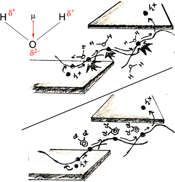
For this discussion, it is elementary to highlight that in polymers, the presence of large amorphous domains results in the occurrence of free volume within the polymer matrix. This makes them particularly vulnerable to the diffusion of chemical and environmental impurities such as oxygen or water. For water-insoluble biodegradable polymers, it has, for instance, been shown that it is the rate of water diffusion that triggers the degradation process and decides if erosion occurs in the bulk or at the surface.[Reference von Burkersroda, Schedl and Goepferich34] Furthermore, even for the most crystalline semiconducting polymers, such as poly(2,5-bis(3-alkylthiophen-2-yl)thieno[3,2-b]-thiophene (PBTTT), diffusion of oxygen and water has been shown to occur and affect their properties.[Reference Boufflet, Han, Fei, Treat, Li, Smilgies, Stingelin, Anthopoulos and Heeney35] Many current-generation conjugated polymers are, nevertheless, designed to be chemically stable (i.e., not biodegradable) with deep-lying HOMO levels ranging between 5.1 and 5.9 eV. In principle, this should stabilize them against oxidation and as a matter of fact, materials with exceptional air stability have commonly been reported.[Reference Park, Lim, Kim, Son and Chung36] However, it has been shown that water and its decomposition into hydroxyl groups, nevertheless, are a key factor that degrade transport properties in these materials.[Reference Zschieschang, Amsharov, Jansen, Kern, Klauk and Weitz37] For a long time, it was thought that water predominantly affects the n-type transport, yet it could be shown that the strong dipole moment of water, in fact, can have a drastic impact on the p-type transport of polymers as well.[Reference Nikolka, Nasrallah, Rose, Ravva, Broch, Harkin, Charmet, Hurhangee, Brown, Illig, Too, Jongman, McCulloch, Bredas and Sirringhaus38] There might be various underlying mechanisms and reactions which cause the generation of charge traps by water molecules. For instance, the application of an electric field has been shown to lead to the splitting of water molecules, which has consequences on the operational stability.[Reference Bobbert, Sharma, Mathijssen, Kemerink and De Leeuw12,Reference Kettner, Zhou, Brill, Blom and Weitz39] However, simply the high dielectric constant and resulting dipole moment of water molecules can also trigger a localization of polarons as soon as water and polaron are brought into proximity. Since charges are predominantly delocalized along the polymer backbone, a small number of water molecules can, hence, be sufficient to detrimentally disturb charge transport (Fig. 3). The resulting disorder broadening can significantly impact the polaron's mobility, however, would not necessarily trigger time-dependent degradation. Such degradation is expected, once water molecules readily diffuse within the polymer microstructure and/or electric fields trigger water splitting. Unfortunately, the large free volume in the microstructure of most conjugated polymers creates ideal conditions for the diffusion of water to occur. Kamerink and coworkers have recently demonstrated how the electrostatic interaction between ensembles of H2O clusters and the backbone of polymers can lead to the formation of hole traps. For a range of p-type polymers with HOMO levels ranging from 5 to 6 eV, the presence of water clusters caused a shift in the energy of the occupied states leading to 0.3–0.4 eV deep shallow traps.[Reference Zuo, Linares, Upreti and Kemerink40] A recent paper by Wetzelaer et al., on the other hand, comes to a different conclusion, and although it clearly identifies the same traps generated by water clusters, their onset was only found to occur for HOMO levels below 6 eV.[Reference Kotadiya, Mondal, Blom, Andrienko and Wetzelaer41] The different conclusions between the two papers can partially be explained by different computational methods used; however, it highlights that a deeper understanding of the role of water, its diffusion as well as its role during the device fabrication and operation is urgently needed.
Illustration of the movement of charges in a plastic semiconductor hindered by the strong electrical dipole of water molecules in vicinity to the backbone (top) and with the water being displaced by an additive (bottom) resulting in unhindered movement of charges.

Degradation of organic optoelectronic devices
So far, we have mainly touched on the general effect that environmental species, such as water and oxygen, can have on the generation of trap states in molecular semiconductors. However, when used in the active layer of an optoelectronic device, the molecular semiconductor is also exposed to additional factors such as an electric field or UV radiation. In reality, the latter can easily be addressed by using a UV-absorbing barrier layer. However, the presence of an electric field is necessary for the transport of charges through the active layer of the device but as an unwanted side effect it also supplies the energy for additional electrochemical reactions to occur. For this reason, an organic optoelectronic device that is stable without an applied voltage (i.e., that exhibits good shelf-life stability), might degrade under constant current operation. For instance, in OLEDs, carrier injection generates positive and negative polarons as well as excitons, which have all been shown to cause electrochemical degradation, deep trap states, interfacial degradation, and reduce the overall OLED lifetime.[Reference Tsang and Adachi42] Some of these factors are associated with damages to the organic materials during the electrical processes that drive light emission,[Reference Song and Lee43] while others are associated with particular device structures. Rather than illuminating these factors one-by-one, it is also clear that OLEDs can achieve lifetimes exceeding 10,000 h once vacuum processed and while using an environmental barrier layer.[Reference Nakayama, Hiyama, Furukawa and Ohtani44] In this Prospective, we, instead, want to focus on the stability of organic devices that are solution processed and where the use of expensive barrier layers might be unfeasible. For this discussion, a good starting point is single carrier diodes made from solution-processed semiconducting polymers. These diodes are particularly susceptible to trapping given that carrier densities in the bulk of such undoped devices rarely exceed 10−15–10−16 cm−3. The presence of trap-limited currents in such diodes typically materialize in steep J–V characteristics exhibiting a slope ≫ 2 when plotted on a log–log scale. Although other factors such as image force lowering and tunneling for injected-limited currents can also affect this slope, these effects can be deconvoluted from trapping by measuring the thickness dependence of the current. Work on both p-type and n-type diodes has demonstrated that charge transport in such single carrier devices is often limited by traps that exhibit a Gaussian energy distribution in the bandgap. For instance, Blom and coworkers could show that for a range of polymers, the number of electron traps is constant at 3 × 10¹⁷ traps per cm3, suggesting a common origin of these traps [Fig. 4(a)].[Reference Nicolai, Kuik, Wetzelaer, de Boer, Campbell, Risko, Brédas and Blom45] They identify the most likely cause of these traps to be related to hydrated oxygen complexes forming trap states close to the polymers' LUMO levels. The trap concentration is also within the same order of magnitude as the obtained carrier densities in these devices making evident the detrimental impact environmental traps can have on charge transport.
(a) Potential configuration of water molecules interacting with the polymer PPV (top) and schematic representation of the energies of the LUMO and the center of the measured trap distribution (bottom); (b) Schematic representation of water molecules in the matrix of the polymer IDT–BT (top) and dn/dE values (representing the density of trap states) for the polymer IDT–BT before and after water was removed through an azeotropic solvent. Reproduced from Ref. [Reference Nikolka, Broch, Armitage, Hanifi, Nowack, Venkateshvaran, Sadhanala, Saska, Mascal, Jung, Lee, McCulloch, Salleo and Sirringhaus10,Reference Nicolai, Kuik, Wetzelaer, de Boer, Campbell, Risko, Brédas and Blom45] with permission from Macmillan Publishers Limited.

However, not only in n-type diodes but also hole-only diodes have been shown to be detrimentally affected by sub-bandgap trap states. The trap levels created by hydrated oxygen complexes as shown in Fig. 4(a) are too remote to affect transport in the deep-lying HOMO levels of polymers. However, it has been shown that the presence of water molecules or water clusters with their strong dipole moments is enough to generate additional trap states in the bandgap close to the HOMO level. For instance, for low-disorder polymers such as IDT–BT, water has been shown to generate a broad trap distribution on the order of 1016 traps per cm3 overshadowing any additional (intrinsic) traps in the material [Fig. 4(b)]. The slow ingestion and diffusion of water, hence, has led to a gradual decrease in the device performance, rendering such polymer diodes highly unstable. By using azeotrope forming solvents, it is, nevertheless, possible to completely remove water traps recovering the sharp band tails measured optically in these materials. Interestingly, by removing water traps from the bulk, space-charge-limited current mobilities approaching the field-effect mobility values are possible. Such diodes, furthermore, exhibit trap-free space-charge-limited current conduction with currents several orders of magnitude higher than before the removal of water traps. The presence of water traps, hence, completely overshadows the intrinsic charge transport properties of these high-performing polymer systems, severely reducing their overall performance.[Reference Nikolka, Broch, Armitage, Hanifi, Nowack, Venkateshvaran, Sadhanala, Saska, Mascal, Jung, Lee, McCulloch, Salleo and Sirringhaus10]
The higher carrier density present in the accumulation layer of field-effect transistors makes these devices intrinsically more robust to bulk trap concentrations ranging between 1017 and 1018 traps per cm3. However, OFETs heavily rely on a trap-free charge transport interface where the accumulation layer is formed and along which charges can move from the source to the drain electrode. One example for the challenges involving this interface is dipolar disorder caused by the mismatch of dielectric constants (and specifically the use of high-k dielectrics) between the molecular semiconductor and dielectric which has been shown to lead to the broadening and generation of trap states.[Reference Sirringhaus46] Additionally, the mismatch in mechanical properties also makes this interface vulnerable to accelerated diffusion of degrading species such as water which can create additional dipolar disorder. Several research groups have independently demonstrated that the diffusion of water molecules at the semiconductor–dielectric interface or inside of nanometer-sized voids in the polymer microstructure is a key factor for reduced operational stability.[Reference Kalb, Haas, Krellner, Mathis and Batlogg47,Reference Mathijssen, Cölle, Gomes, Smits, De Boer, Mcculloch, Bobbert and De Leeuw48] This is generally measured as a shift in the transistor's threshold voltage V th. For instance, Bobbert et al. have shown that redox reactions involving water and a subsequent exchange of mobile charges in the semiconductor with protons in the gate dielectric is the key mechanism responsible for the reduced operational stability of polymer OFETs.[Reference Bobbert, Sharma, Mathijssen, Kemerink and De Leeuw12] The underlying mechanism can, for instance, explain the stretched exponential-like time dependence which is observed for the degradations of OFETs in operando. Further evidence for the key role of water not only in the generation of sub-bandgap trap states but also for the reduced operational stability of molecular FETs could recently been shown by Weitz and coworkers. Performing stress measurements in a vacuum Cryostat, the group was able to show that stress-related threshold voltage shifts can be entirely suppressed for temperatures below 275 K (Fig. 5). The authors argue that, in fact, H3O+ and OH− stemming from the autoionization of liquid water is the universal extrinsic trap, which is responsible for the observed threshold voltage shifts and device degradation. When freezing out this autoionization process at low temperatures, devices with exceptional stability could be demonstrated with extrapolated threshold shifts below 1 V even after 6 days of continuous stressing. This is comparable to many inorganic FET technologies such as oxide semiconductors or amorphous silicon and unambiguously demonstrates that (i) the key role that water plays in reducing the operational stability of OFETs and (ii) the stability that can, in principle, be obtained in solution-processed high-performance polymer semiconductor devices. This demonstrates that a clear need arises to completely displace water molecules from the polymer film and nip water-based degradation processes in the bud.
Threshold voltage shift (ΔV th) measured at various bias-stress conditions for a stress duration of 3600 s. The dashed sloped lines are fits to the data in the high-temperature regime. Reproduced from Ref. [Reference Kettner, Zhou, Brill, Blom and Weitz39] with permission from the American Chemical Society (ACS).

Operation in aqueous electrolytes
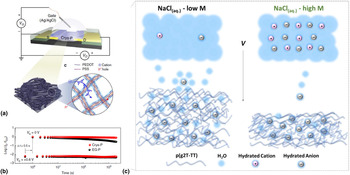
So far, we have discussed the role of water as a degrading species for organic devices. Especially, for low-disorder and high-mobility conjugated polymers, the presence of water was unraveled to be the key species degrading the operational stability as well as a major contributor leading to a reduction in shelf-life stability. This, in turn, raises the critical question how devices that operate in aqueous electrolytes, such electrolyte-gated transistors (EGOFETs) or electrochemical transistors (OECTs), can show highly reliable performances. In fact, devices such as OECTs are, in principle, subject to the same degradation pathways as conventional OFETs and additionally have to be electrochemically oxidized and reduced requiring exceptional electrochemical stability over many cycles.[Reference Rivnay, Inal, Salleo, Berggren and Malliaras49,Reference Giovannitti, Nielsen, Sbircea, Inal, Donahue, Niazi, Hanifi, Amassian, Malliaras, Rivnay and McCulloch50] It should be noted though that, in contrast to conventional OFETs, the operational voltages of OECTs are only on the order of a few hundreds of mV which at no point exceeds the electrochemical window of water splitting and might help to prevent rapid stress-related degradation as seen in many OFETs. Yet, unsurprisingly, there have been several studies on the stability and degradation of common OECT materials looking at the effect of electrolytes, exposure to oxidants, and reducing agents or biological counterions.[Reference Green, Lovell and Poole-Warren51,Reference Thaning, Asplund, Nyberg, Inganäs and Von Holst52] All these studies find that materials, such as poly(3,4-ethylenedioxythiophene):poly(styrenesulfonate) (PEDOT:PSS), exhibit high stabilities for several days, and 100–1000 s of consecutive cycles, however, show an eventual drop in the device performance [Figs. 6(a) and 6(b)].[Reference Asplund, Nyberg and Inganäs53] For instance, when operated and switched repetitively, PEDOT:PSS OECTs have been shown to exhibit a gradual drop in on-current over the course of 1 h which is at a level not too dissimilar seen in OFETs when stressed.[Reference Nikolka, Nasrallah, Rose, Ravva, Broch, Harkin, Charmet, Hurhangee, Brown, Illig, Too, Jongman, McCulloch, Bredas and Sirringhaus38,Reference Kim, Kim, Kim, Kim, Lee, Lee, Kim, Park, Lee, Rivnay and Yoon54] Increasing the overall crystallinity of PEDOT:PSS has been demonstrated to improve these trends but does not suppress this degradation entirely. Recently, Inal and coworkers could show that an effect that is overlooked in the cyclic stability of accumulation-type OECTs is the water taken up by the film during device operation [Fig. 6(c)].[Reference Savva, Cendra, Giugni, Torre, Surgailis, Ohayon, Giovannitti, McCulloch, Di Fabrizio, Salleo, Rivnay and Inal13] It was demonstrated that the hydration shell of dopant anions leads to structural and morphological changes occurring in the film upon electrochemical doping and is responsible for lowering the overall device speed and cyclic stability. A similar observation has been made by the group of Ginger, who argue that the loss of connectivity in amorphous polymer regions upon hydration is responsible for reduced charge carrier mobilites.[Reference Flagg, Bischak, Onorato, Rashid, Luscombe and Ginger55] This clearly shows that the adverse effect of water molecules penetrating the active semiconductor cannot be underestimated. Interestingly, for depletion-type OECTs, this phenomenon has not been observed so far, and it is rather assumed that in such devices, hydration is generally beneficial for device operation.[Reference Savva, Cendra, Giugni, Torre, Surgailis, Ohayon, Giovannitti, McCulloch, Di Fabrizio, Salleo, Rivnay and Inal13] An explanation for this might be found in the particular microstructure of depletion-type OECT materials such as PEDOT:PSS. Here, the hydrophobic PEDOT core is surrounded by a shell of hydrophilic PSS. The electronic charge transport process, on the other hand, is dominated by hopping between sub-micrometric domains of PEDOT separated by insulating layers of PSS.[Reference Colucci, Faria, Santos and Gozzi56] Therefore, the role of PSS in spatially separating the electronic charge transport process from ingested water clusters is one potential explanation for the improved robustness of PEDOT:PSS OECTs over the accumulation-type material. Additionally, the high conductivities and beneficial role of polarons stabilizing the transport along the PEDOT backbone can also contribute to this improved stability. Further evidence for the important role that PSS plays in the stability of depletion-type OECTs is the observation that aging PEDOT:PSS in water for extended time periods leads to loss of PSS chains making the films more hydrophobic.[Reference Duc, Vlandas, Malliaras and Senez57] Therefore, water can be expected to preferably interact with PSS chains which might be sufficient to prevent its detrimental effect on the charge transport along the PEDOT backbone. The removal of PSS could also explain the slow and steady degradation of charge transport properties seen for depletion-type OECTs when cycled over extended times [Fig. 6(b)]. Nevertheless, it should also be pointed out that cyclic stability requirements for OECTs are less stringent than for OFETs which must operate for extended periods under constant current stress at high voltages. It should also be highlighted that charge transport processes in mixed ionic–electronic conductors, such as PEDOT:PSS, are complex with both charges and ions moving at different mobilities and the doping and de-doping processes resulting in constant changes to the polymer microstructure.[Reference Cendra, Giovannitti, Savva, Venkatraman, McCulloch, Salleo, Inal and Rivnay58] Due to the focus of this Prospective, we have only picked water as one cause for degradation and addressing stability issues in OECTs will require a holistic understanding of all these degradation process.
(a) Structure of a PEDOT:PSS OECTs schematic diagram of the hole and ion transport in PEDOT:PSS; (b) normalized current on/off ratio traced during the repeated VG switching of a PEDOT:PSS PECT for 2000 cycles; (c) schematic showing the polymer-electrolyte interface and the differences in the swelling behavior of the film in low- and high-concentration electrolyte. Reproduced from Ref. [Reference Savva, Cendra, Giugni, Torre, Surgailis, Ohayon, Giovannitti, McCulloch, Di Fabrizio, Salleo, Rivnay and Inal13,Reference Kim, Kim, Kim, Kim, Lee, Lee, Kim, Park, Lee, Rivnay and Yoon54] with permission from Macmillan Publishers Limited and the American Chemical Society (ACS).

Given that the cyclic penetration of the active semiconductor of an OECT with hydrated ions and the presence of strong dipoles within the polymer matrix has a negative impact on OECT speed and performance, it is interesting to compare OECTs to the performance of EGOFETs. An EGOFET operates very similarly to an OFET with the key difference that the gate dielectric is replaced by an electrolyte. The two electrical double layers (EDLs) that are formed at both gate electrode/water and water/OSC interfaces then form the effective gate-insulator layer.[Reference Zhang, Leonardi, Casalini, Temiño and Mas-Torrent59] For this reason, EGOFETs are an excellent tool to understand some of the intrinsic interactions taking place at the polymer-electrolyte interface without having to consider the complex bulk and ionic interactions that dominate the operation of an OECT. Unfortunately, EGOFETs are notoriously difficult to realize since exposure to aqueous electrolytes can lead to swelling of the active semiconductor and, hence, controlling the accumulation layer becomes a challenge. Despite these challenges, there has been some success showing that it is possible to operate transistors in the narrow electrochemical stability window where transfer curves do not exhibit signs of ionic doping from the electrolyte which can be associated to clean EGOFET operation.[Reference Kergoat, Herlogsson, Braga, Piro, Pham, Crispin, Berggren and Horowitz60] Torsi and coworkers have used such devices to show the ultra-accurate detection of molecular analytes enabled by the high sensitivity of the EDL to any disruption caused by a biomarker binding to one of the interfaces.[Reference Macchia, Manoli, Holzer, Di Franco, Ghittorelli, Torricelli, Alberga, Mangiatordi, Palazzo, Scamarcio and Torsi61] However, it should be noted that many EGOFETs reported up to date exhibit a clear signal drift when operated over several minutes or hours and, thus, have to be considered less stable than OECTs.[Reference Mulla, Tuccori, Magliulo, Lattanzi, Palazzo, Persaud and Torsi62] Schmoltner et al. have argued that this observed instability and drift can be ascribed to the electrolysis of water at the electrolyte/semiconductor interface. This is founded on the observation that drift is minimal when the gate of the transistor is off which suggest a main device degradation pathway that is very similar to that of an OFET.[Reference Schmoltner, Kofler, Klug and List-Kratochvil63] This observation highlights that even the small voltages used in these electrolyte-gated devices cannot entirely prevent water-related degradation when currents are applied over an extended period. However, it is also clear that more research is needed to fully understand the charge transport processes in EGOFETs. Particularly, the role that swelling of the active semiconductor and transient changes in the formation of the ionic double layer play in affecting the overall signal drift and associated device stability.
Overcoming stability challenges
From our previous discussion, it is evident that water plays a key role in degrading the operational stability of molecular semiconductors. To overcome water-related stability challenges for the long-term and mass-market application, therefore, the various water degradation pathways must be addressed independently. From our discussion so far, a clear observation is that charge carrier density plays an elementary role in determining the susceptibility of an optoelectronic device to water-related trapping. For instance, for single carrier diodes, where charge carrier densities are low (10−15–10−16 cm−3), water-related traps exhibit the biggest impact on the overall device. In this case, the intrinsic device performances are being masked and charge carrier mobility values reduced by several orders of magnitude.[Reference Nikolka, Broch, Armitage, Hanifi, Nowack, Venkateshvaran, Sadhanala, Saska, Mascal, Jung, Lee, McCulloch, Salleo and Sirringhaus10] For OFETs and EGOFETs where carrier densities are two orders of magnitude higher than in a diode, water traps can be seen to mostly affect the sub-threshold performance or the operational stability.[Reference Nikolka, Schweicher, Armitage, Nasrallah, Jellett, Guo, Hurhangee, Sadhanala, McCulloch, Nielsen and Sirringhaus64] In OECTs where the electrochemical doping leads to high bulk charge densities and, hence, more effective trap passivation,[Reference Hulea, Brom, Houtepen, Vanmaekelbergh, Kelly and Meulenkamp65] it is mostly the strong dipole and morphological changes induced by significant amounts of water that leads to slower device operation and eventual device degradation. This suggests that the trap densities generated by water will rarely exceed 1017 traps per cm3, and as a result, these trap states can be filled once a higher carrier density is available (Fig. 7). For OECTs and EGOFETs which rely on the presence of water, a challenge, therefore, remains to prevent or alternatively control excessive swelling and water uptake in the next generation of materials. One option is the study of new depletion-type OECT materials with alternative ionomers to PSS which might offer further improved stability in aqueous environments and better and more efficient passivation of the conjugated polymer backbone against the detrimental proximity of water dipoles. These lessons might also be translated to accumulation-type OECT materials where filler materials could be used to serve a similar purpose. For most other optoelectronic devices, where carrier densities are lower, it is a key challenge to exclude water from processing and prevent water ingestion altogether. In OLEDs, this has been achieved by processing devices in a water-free vacuum environment and using highly sophisticated barrier layers with upper limits for water vapor transmission rate (WVTR) in the order of 10−6 g/m2/day.[Reference Paetzold, Winnacker, Henseler, Cesari and Heuser68] For glass-based OLEDs displays, these barrier layers are usually comprising epoxy-based adhesives in combination with a getter for water (i.e., a highly hygroscopic material) that captures water vapor. Alternatively, fillers are used which can enhance the overall properties of such barriers allowing them to meet the highly stringent encapsulation requirements.[Reference Steckel, Khan and Drolet69] Although these give some effective protection, it requires complex manufacturing processes which do not fully agree with the low-cost solution-processed manufacturing that makes molecular semiconductors attractive in the first place.
Approaches of overcoming water-induced traps in molecular semiconductors: (a) pivotal role of charge carrier density in filling water-induced trap states in a range of optoelectronic devices. Electrodes are represented as yellow, insulators are gray, and active semiconducting layers are represented in green; (b) method of overcoming water-induced traps in polymer diodes by diluting the semiconductor with an insulating polymer; (c) achieving high threshold stability in molecular OFETs by using multilayer gate dielectrics; (d) enabling stable diodes by using filler additives that displace water. Reproduced from Ref. [Reference Nikolka, Broch, Armitage, Hanifi, Nowack, Venkateshvaran, Sadhanala, Saska, Mascal, Jung, Lee, McCulloch, Salleo and Sirringhaus10,Reference Abbaszadeh, Kunz, Wetzelaer, Michels, Crăciun, Koynov, Lieberwirth and Blom66,Reference Jia, Fuentes-hernandez, Wang, Park and Kippelen67] with permission from Macmillan Publishers Limited and the American Association for the Advancement of Science.

Therefore, different approaches are required to reduce the susceptibility of polymer devices to bulk traps. Given that water is almost impossible to exclude from solution-based device manufacturing processes (it is present in the synthesized materials, dielectrics, gets absorbed on surfaces, and even in anhydrous solvents, it will be present at low concentrations), new ways of mitigating its negative impacts are needed. An example for such an approach is the work by Blom and coworkers who suggested a general concept of how charge carrier trapping can be suppressed by dilution of the transport and trapping sites.[Reference Abbaszadeh, Kunz, Wetzelaer, Michels, Crăciun, Koynov, Lieberwirth and Blom66] This idea is conceptually very similar to that one of polymer extender fillers used in the chemical industry where a cheaper compound is used to occupy space in the polymer matrix and thus lower the formulation cost. An alternative option is to use additives or functional fillers that are able to actively replace or remove water from polymer films altogether. This has been shown to result in a significant reduction in the water-induced trapping as well as an improvement in the operational stability.[Reference Nikolka, Broch, Armitage, Hanifi, Nowack, Venkateshvaran, Sadhanala, Saska, Mascal, Jung, Lee, McCulloch, Salleo and Sirringhaus10,Reference Nikolka, Schweicher, Armitage, Nasrallah, Jellett, Guo, Hurhangee, Sadhanala, McCulloch, Nielsen and Sirringhaus64] Here, a challenge remains large area processing and guaranteeing sufficient incorporation of usually poorly soluble additives in the polymer microstructure.[Reference Nikolka, Schweicher, Armitage, Nasrallah, Jellett, Guo, Hurhangee, Sadhanala, McCulloch, Nielsen and Sirringhaus64] The use of solvent treatments that remove water ingested during processing through the formation of nazeotropes is another highly effective approach.[Reference Nikolka, Schweicher, Armitage, Nasrallah, Jellett, Guo, Hurhangee, Sadhanala, McCulloch, Nielsen and Sirringhaus64,Reference Jacobs, Wang, Hafezi, Medina-Plaza, Harrelson, Li, Augustine, Mascal and Moulé70] Nevertheless, the benefits of this water-trap removal technique will only persevere, as long as the back-diffusion of water is prevented by using additional barrier layers. For the application in OFETs, Kippelen and coworkers have shown an alternative engineering approach of using sequential layers of both organic and inorganic gate dielectrics that are able to compensate water-induced threshold voltage instabilities during stressing.[Reference Jia, Fuentes-hernandez, Wang, Park and Kippelen67,Reference Wang, Fuentes-hernandez, Yun, Singh, Dindar, Choi, Graham and Kippelen71] In such bilayer devices, the second dielectric layer compensates the threshold voltage shift induced by the water-related trapping of carriers.[Reference Zhao, Tang, Li, Liu and Guo72] This mechanism enabled low-voltage OFETs with threshold stabilities below 0.2 V during 7 days of stressing which is comparable to other commercial TFT technologies such as a-Si TFTs used in LCD displays.[Reference Jia, Fuentes-hernandez, Wang, Park and Kippelen67] However, this threshold voltage compensation requires careful optimization of the various layers involved and the underlying mechanism is still elusive. A potential explanation is the compensation of water-induced threshold shifts through dipolar reorientation in the second (usually high-k) dielectric, which has also been observed for polymer dielectrics with ionic impurities.[Reference Wang, Lee, Kong, Pfattner, Schweicher, Nakajima, Lu, Mei, Lee, Wu, Lopez, Diao, Gu, Himmelberger, Niu, Matthews, He, Salleo, Nishi and Bao73,Reference Kong, Pfattner, Chortos, Lu, Hinckley, Wang, Lee, Chung and Bao74] These approaches clearly show that there are workarounds to address the detrimental effect of water traps in molecular semiconductors that can enable stability levels required for mass-market adaptation.
Beyond molecular semiconductors: water in perovskites and CNTs
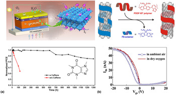
The detrimental role of water on both charge transport properties and stability should not be considered an isolated problem occurring only in molecular semiconductors. Here, we want to give two brief examples of how other solution-processed hybrid organic–inorganic material classes are plagued by water-induced trapping and how the lessons learned from molecular semiconductors might be transferable to these materials in the future. Of course, each one of these materials is complex in their nature; therefore, here we can only give a brief overview of some relevant material classes and water-related trapping phenomena. One such an example is perovskites where moisture-induced degradation has been shown to represent an Achilles heel significantly reducing the overall lifetime that can be obtained in solar cells.[Reference Solanki, Lim, Mhaisalkar and Sum11] It should be noted that charge transport in perovskites is affected by a range of different factors such as trapping induced by vacancies (e.g., of iodine), the presence of ions and grain boundaries as well as grain sizes. Furthermore, due to water acting as a solvent for most perovskites, its role can be considered far more complex than in molecular semiconductors that are insoluble in water. Nevertheless, from the broad range of literature published on this topic, there is a clear consensus that an uncontrolled amount of water is by far one of the most detrimental factors restricting long-term device operation. Interestingly, recently it has been shown that when incorporating caffeine into the microstructure of MAPbI3 and CsFAMAPbI3 perovskite solar cells, both the heat stability as well as moisture stability can significantly be improved (Fig. 8).[Reference Wang, Xue, Meng, Lee, Zhao, Sun, Cai, Huang and Wang75] Interestingly, this concept is the same as the approach of using fillers in molecular semiconductors to either dilute traps or displace water molecules. For the given case, the authors associate the improved stability to caffeine molecules locking onto the perovskite crystal and stabilizing the grain boundaries which prevents the material from degradation triggered by heat and moisture. It should, however, be noted that caffeine is also well known to strongly interact with water which might contribute to the improved stability in a similar fashion to the mechanism by which small molecular additives interact with water in polymers.[Reference Tavagnacco, Schnupf, Mason, Saboungi, Cesàro and Brady79] Although the underlying mechanism might indeed vary, this example, nevertheless, exhibits the overlap to molecular electronics and the possibility of using small molecular additives in perovskites. The use of polymer fillers in perovskites might, therefore, offer new routes to overcoming stability shortfalls in this highly promising materials class.
(a) Schematic diagram of the various factors that can degrade MAPbI3 perovskite solar cells. The addition of small molecules such as caffeine leads to a significant improvement in ambient stability; (b) schematic diagram of the polymer wrapping process used to sort CNTs. Residuals of the wrapping polymer will remain in deposited films of CNT networks; stability of CNT transistors in the dry and ambient environment showing the impact of water-generated traps. Reproduced from Ref. [Reference Wang, Xue, Meng, Lee, Zhao, Sun, Cai, Huang and Wang75–Reference Berton, Lemasson, Hennrich, Kappes and Mayor78] with permission from Macmillan Publishers Limited, the Royal Society of Chemistry, Cell Press, and the American Chemical Society (ACS).

A different class of materials that are well known to be affected by trapping from water molecules are CNTs. It should be noted here that we can indeed count solution-processed semiconducting CNTs amongst the class of organic–inorganic hybrid material; they are often sorted using a polymer wrapping process, and it can, therefore, be assumed that a significant proportion of these wrapping polymers will still be present in the final CNT network.[Reference Arnold, Green, Hulvat, Stupp and Hersam80] It has been demonstrated by several groups independently that such networks of CNTs are highly effective humidity sensors where gradually increasing resistivity for increasing humidity values have been observed.[Reference Arunachalam, Izquierdo and Nabki81] The underlying mechanism for the observed humidity sensitivity was linked to water molecules donating electrons to the p-type CNT networks and thus reducing the overall number of charge carriers.[Reference Zahab, Spina, Poncharal and Marlière82] These results highlight that akin to polymer semiconductors with their soft microstructure, networks of CNTs are highly susceptible to the fast diffusion of water. However, whereas this feature is attractive for highly sensitive humidity detectors, in other CNT-based devices this might not be the case. For instance, it has been demonstrated for CNT transistors that water has an overshadowing impact on device performance causing hysteresis and trapping.[Reference Kim, Javey, Vermesh, Wang, Li and Dai76,Reference Estrada, Dutta, Liao and Pop83] This effect can partially be mitigated by using a polymer coating layer that encapsulates the network of CNTs and, furthermore, reduces the amount of free volume that can be occupied by water.[Reference Kim, Javey, Vermesh, Wang, Li and Dai76] From our discussion on conjugated polymers, it should, nevertheless, be clear that such an approach cannot guarantee stability levels required for mass-market applications. This shows that there is indeed a clear need to transfer some of the lessons learned from polymer FETs to CNT transistors.
Outlook and conclusions
From our discussion, it is clear that water plays a fundamental role in degrading both the performance and stability of a range of molecular and hybrid semiconductor devices. We arrived at the unambiguous conclusion that water-induced traps need to be fundamentally addressed to unlock the intrinsic capabilities of these materials and enable them to be used in mass-market applications. The current route of using barrier layers in the OLED industry, unfortunately only works efficiently once devices are vacuum processed and encapsulated in these environments. For solution processing, this is not an option, as the degrading species like water are already present in the film due to the nature of processing. We have reviewed some of the fundamental mechanisms by which water can create trap states or degrade the performance of a range of semiconducting devices ranging from diodes to electrolyte-gated transistors. A key take-away from our analysis is the strong dependence of susceptibility to traps created by water molecules on charge carrier density. We also reviewed some mechanisms of addressing water traps that either compensate for the detrimental effects of water traps or alternatively dilute traps or displace and remove water molecules altogether. Many of these approaches offer a potential solution to improve the stability levels of molecular and hybrid semiconductors to be comparable to competing for inorganic materials. In this respect, a lot of lessons can be learned from work done in the polymer industry on using additives and fillers. More research needs to be done to find materials and fillers that are able to prevent long-term degradation in mass-market products. Nevertheless, current research clearly shows that it is possible to eliminate the effects of water trapping in promising molecular and hybrid material classes; even though insufficient stability remains a concern, it is also clear that in the future, there are routes to address this problem. This will enable these highly promising material systems to unfold their true potential in a broad range of optoelectronic and sensing applications.
Acknowledgments
M.N. acknowledges financial support from the European Commission through a Marie-Curie Individual Fellowship (EC Grant Agreement Number: 747461). M.N. thanks Dr. Deepak Venkateshvaran, Dr. Ulrike Kraft, and Dr. Guillaume Schweicher for help with illustrations and proof reading.


 Open access