


Introduction
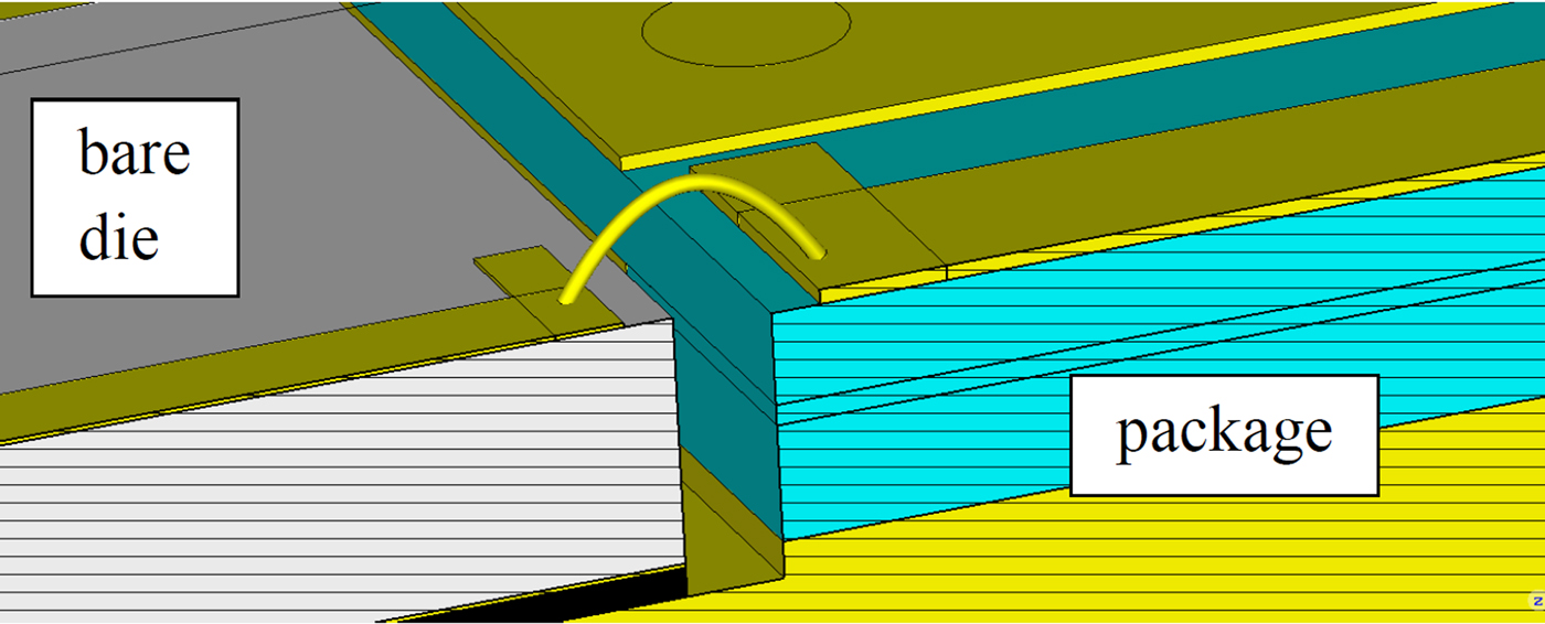
The increasing structural accuracy of conventionally manufactured printed circuit boards (PCBs) with wet-chemical etching processes allows more and more millimeter wave applications to be realized directly on circuit boards. What was previously only achieved directly on the semiconductor or on ceramic chip carriers (e.g. couplers or filters) can now be inexpensively and individually integrated into the PCB. By packaging with organic substrates, radio frequency (RF) chips for applications up to 67 GHz can be integrated in standard PCB substrates [Reference Roehrl, Jakob, Bogner and Hageneder1]. In addition to the PCB connector, the signal path on the PCB and the PCB-package transition, the connection of the chip itself pushes its limit. Broadband applications (e.g. for signal generators with 1.00 mm coaxial system) require transitions with low return loss up to 110 GHz. Here, the conventional wire bonding technology (Fig. 1) reaches its limits. By differential signal routing, a broadband transition between package and chip can be expanded up to 67 GHz [Reference Roehrl, Jakob, Bogner, Hageneder and Zorn2]. Narrowband transitions in this frequency range are possible. Broadband single ended transitions generate much earlier unacceptable reflections. Additive built transitions using aerosol jet printing technology (AJT) have a significantly lower inductive character and, therefore, should allow transitions with lower reflection coefficients.
Bonded package – chip transition (schematic, cross-section).
Aerosol jet technology
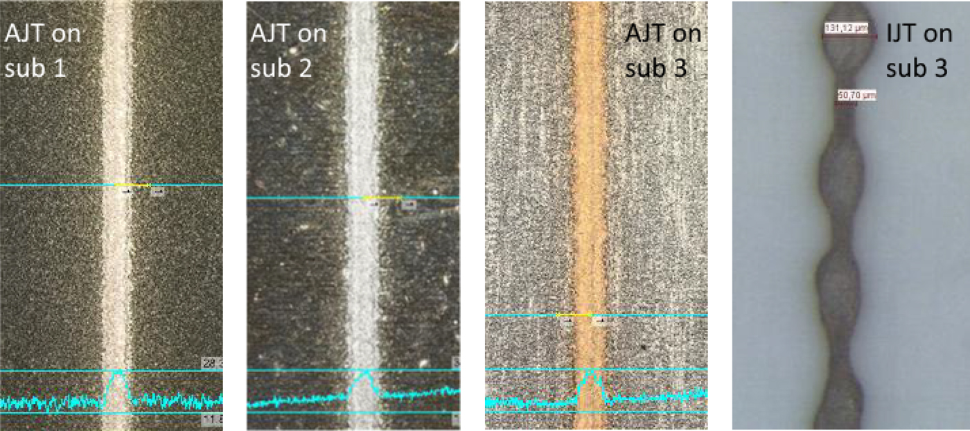
Using the aerosol jet (AJ) technology, a variety of materials can be deposited selectively and maskless. In the field of PCB technology, the additive method has distinct advantages with respect to the achievable structure accuracy in contrast to the traditional subtractive wet chemical etching process. Here, structures can be realized down to 10 µm line width and 10 µm space. Since the method works contactless, it can create structures on almost any surface or shape. Compared with inkjet technologies (IJT), AJT allows narrower and thinner lines. PCBs for RF applications can be made of different PCB materials. In principle, a distinction is made between three groups: FR-4 materials with ceramic fillers (substrate 1 in Fig. 2), Polytetrafluoroethylene-based materials (substrate 2 in Fig. 2) and liquid crystal polymer materials (substrate 3 in Fig. 2). These materials differ in their surface properties partly clear. Unlike IJT, however, AJ technology has the advantage that it adheres to all three material groups (Fig. 2) without having to change the manufacturing parameters significantly. In addition, the layer thickness and conductor width can be set much more precisely than with inkjet, because the proportion of volatile components in AJ inks is significantly lower than in inkjet inks. This is especially important for multiple prints.
AJT and IJT printed 50 µm lines on different RF PCB substrates.
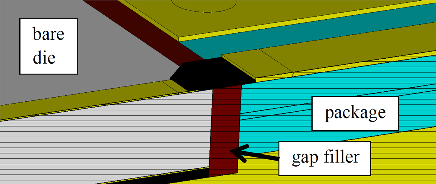
Furthermore, the morphology is independent of the printing direction [Reference Seifert, Sowade, Roscher, Wiemer, Gessner and Baumann3]. The use of AJT to generate lines of silver ink is well-documented [Reference Goth, Putzo and Franke4, Reference Kaestle, Hoerber, Oechsner and Franke5]. Thus, on the one hand, the RF characterization of AJ printed lines is published [Reference Cai, Pavlidis, Papapolymerou, Chang, Wang, Zhang and Wang6–Reference Qayyum, Abt and Papapolymerou10] and on the other hand, the AJT has been used to connect chips [Reference Stoukatch, Laurent, Dricot, Axisa, Seronveaux, Heusdens and Destiné11]. Nevertheless, to the authors’ knowledge, there is still no public research to connect chips to circuit boards (Fig. 3) for millimeter wave applications.
Printed package – chip transition (schematic, cross-section).
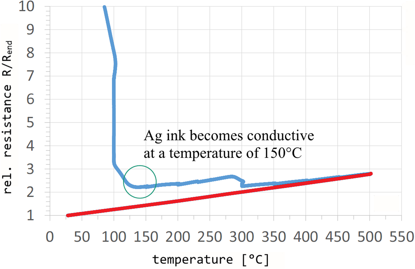
For printing chip transitions, an AJ Printer with pneumatic atomizer (fine feature deposition head with heater and shutter; ±6 µm accuracy motion system; feature size to 10 µm) provided by Fraunhofer IKTS was employed. The ink applied is a commercially available silver nanoparticle ink (Paru PG-007) with a silver content of 70% per weight and a surface tension of 50 mN/m. After depositing, the nanoparticle ink requires a thermal post-treatment to enable the solvent to evaporate and to achieve good electrical conductivity by initializing sintering of the particles. Generally, it can be said, the higher the sintering temperature, the better the electrical conductivity. For usual PCBs it is important that the temperature is not above 170°C. Higher sintering temperatures for best reliability, e.g. 600°C and above [Reference Horibe and Yoshida8], would destroy the PCB substrates. Figure 4 shows the achievable relative electrical resistance as a function of the sintering temperature of the analyzed silver ink and the relative resistance of Rend depending on temperature (cooling curve). The measurement results were obtained experimentally by measuring the resistance of a printed line during the sintering and cooling phase. Since the ink already reaches its 2–3 times minimum resistance (Rend) value at a temperature of 150°C, the ink is very suitable for use on organic PCBs. R end is the resistance of the silver ink at room temperature when sintering with a temperature of 500°C. The temperature coefficient of resistance (TCR) of the AJ silver ink (3.77×10³ 1/K) is nearly the same as the TCR of a pure silver bulk (3.8×10³ 1/K). The TCR was determined by the cooling curve of the resistance. By comparison, inkjet inks have a twice as high electrical resistance due to their lower silver content (<50% compared with AJ inks).
Achievable electrical resistance versus sintering temperature of Ag Ink.
Nearly as important and challenging as the conductive chip connection is the filling of the gap between chip and package with a nonconductive material. Due to dimensional fabrication tolerances of the bare die and primarily the PCB, the gap between bare die can have between 50 and 200% of its nominal value. In our case, the gap has a nominal width of 100 µm and a depth of 290 µm (height of bare die, metallization, and conductive adhesive). It is of particular importance that the gap is filled in a precisely defined way. The gap filler material must neither overflow nor fill the gap only partially. Therefore, a camera-supported individual filling of each gap is applied. The filler used was the commercially available Epotek H70-175 adhesive. With a particle size of 20 µm it is easy to dose and still liquid enough to evenly fill the gap.
Mechanical stability in comparison with bond technology
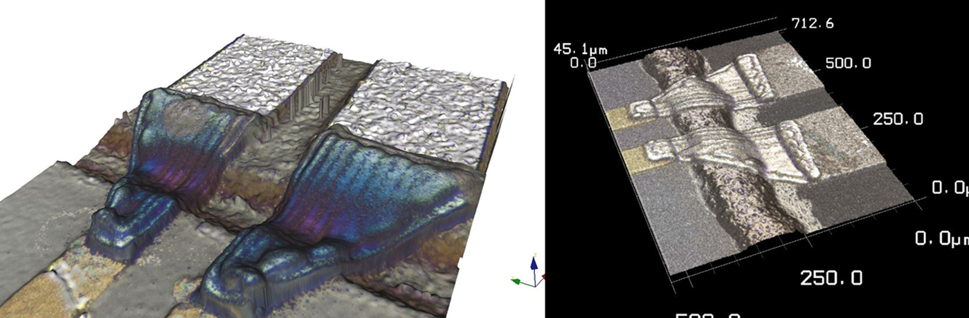
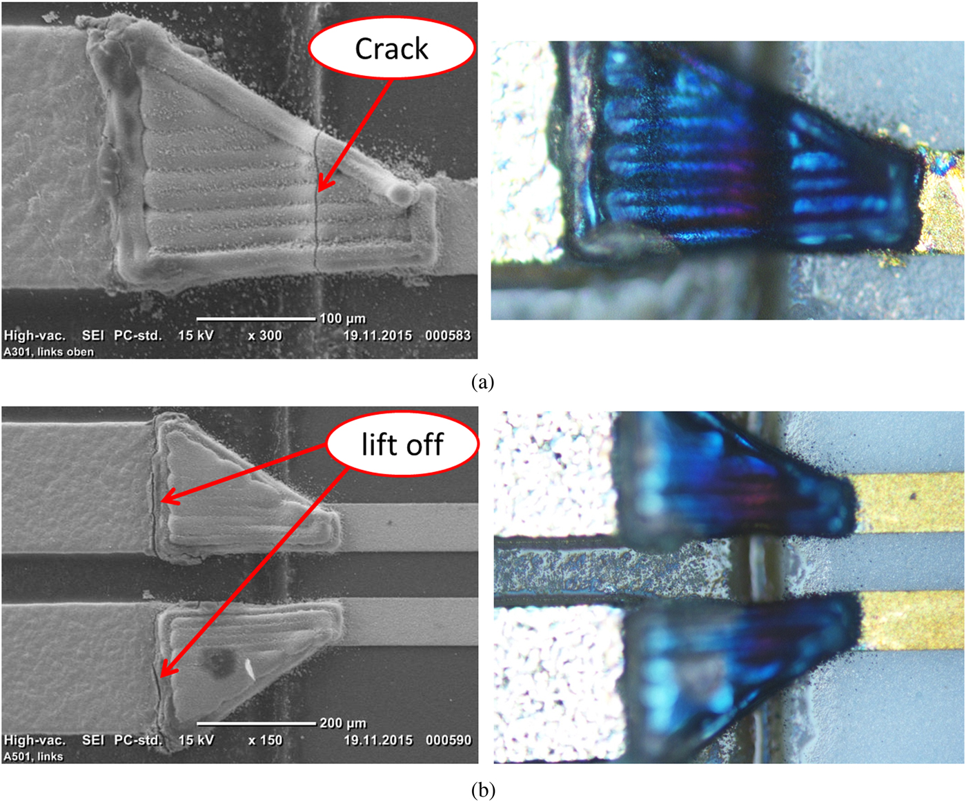
An important point is first how the gap between bare die and PCB is filled. Optimum mechanical stability is achieved when the gap is filled slightly over-inflated so that the substrate for the ink only has flat or obtuse angles (Fig. 5). If there are right or even acute angles, the printed AJ lines may lift off (due to different thermal expansion coefficients of PCB, gap filler, and bare die) or form cracks. Both lead to discontinuities on the transmission lines, which make signal transmission impossible.
Incorrect (left) and correct (right) filled gap.
Cracks are particularly critical as they are extremely hard to see visually by optical microscopes (Fig. 6, right). Only a technology like scanning electron microscopy reveals a crack or lift off in the AJ line (Fig. 6, left).
Failure images of AJ printed lines caused by wrong gap filling.
In contrast to bonding wires, however, the surface finish of the contact points to be connected (PCB and bare die) can be selected almost arbitrarily. Thus, for example, a cheap and highly conductive silver surface can be used on the PCB substrate instead of special bondable metallization like ENEPIG®.
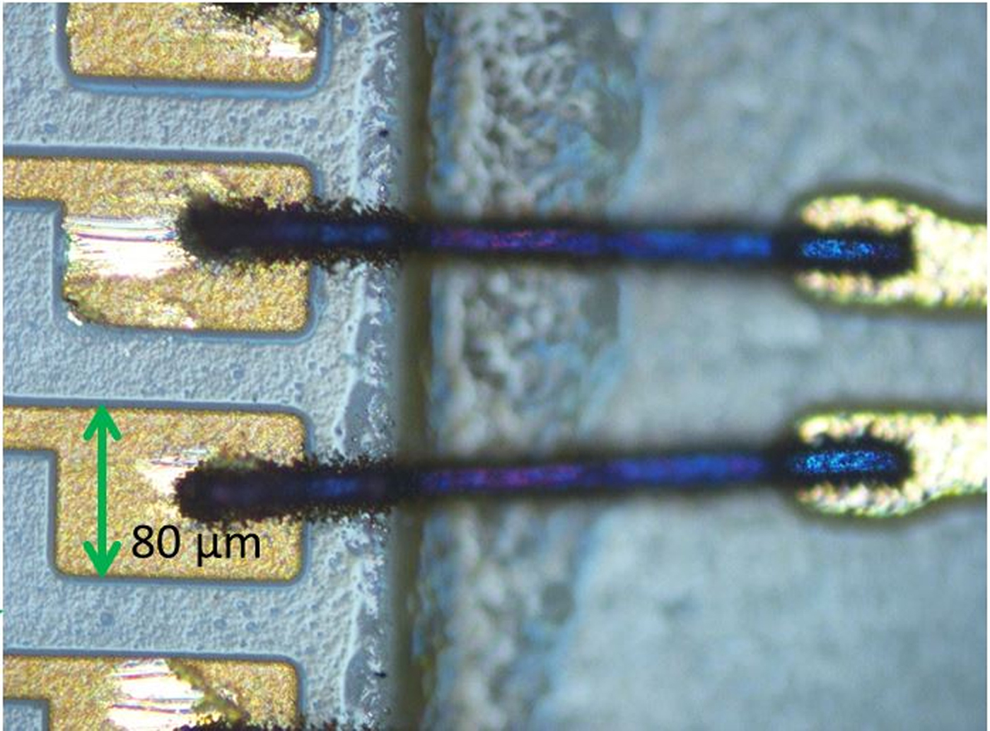
It is only important that the surface is not too smooth (roughness >0.2 µm) and that the coefficient of thermal expansion (CTE) mismatch of the materials used (bare die, gap filler, PCB) is not too high. Moreover, there is no restriction in bond pad size. Common bond pads should not have a size below 80 µm×80 µm, otherwise the pad can be destroyed during the bond process. AJ pads can have a much smaller size (Fig. 7) because there is no mechanical stress during AJ process.
Common wire Bond Pads connected via AJ.
In addition, it is important that the gap filling material is fully cured before the AJ print so that no subsequent stress is built upon the silver ink. The last point to keep in mind is the number of deposited ink layers for a connection. Depositing too few layers, the conductance of the connection reduces too much. If one applies too many, the ink cannot compensate the CTE mismatch between bare die and PCB any more leading to the failures shown in Fig. 6. For the materials used here, the most stable transitions were created with three print passes and a final ink thickness of 16–17 µm. In this case, the horizontal tolerances are smaller than 3 µm. The AJ Printer can print lines with a velocity of 4– 6 mm/s. This means a printing time of nearly 15 s/transition with one printing nozzle, which is significantly higher than conventional well-optimized wire bonders.
Electrical RF characterization of gap filler material and silver ink
For the most mechanically stable configuration (three print passes, 150°C sintering temperature for 1 h) a bulk resistance of 3.5 mΩ/sq was achieved. This is almost 4 times as high as that of a comparable copper line (0.88 mΩ/sq). However, the lines can be realized very smoothly and with an accuracy of ±3 µm, which makes AJ ideal for impedance critical applications. Conventional wet-chemically etched copper lines can currently only be realized with an accuracy of ±5 µm with high-end technology [Reference Hassel12].
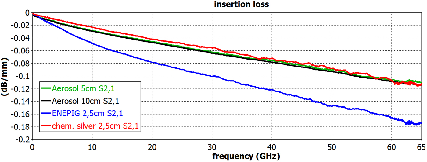
Looking at the RF performance of AJ printed silver ink lines, they achieve similar transmission loss values as silver coated copper wires (Fig. 8). The reason is that surface roughness and dielectric losses dominate the losses in the GHz range and the reduced bulk resistance has virtually no influence. It is also striking that the AJ lines thus also have a significantly lower insertion loss than lines with bondable surfaces (e.g. ENEPIG). ENEPIG [Reference Hofstetter13] is an end surface with a relatively thick nickel layer (4–7 µm), which is required for gold wire bonding. The relative hard nickel allows the bond wires to form a robust connection to the copper line on the PCB. Silver lines on the PCB are not suitable for bonding applications because they are too soft and do not bond sturdily enough to the bond wires. Tests, that simulate soldering procedures in reflow workstations with temperatures up to 268°C (three cycles á 6.33 min) did not change the RF performance of the AJ lines. A measurement of samples stored for 12 months in room atmosphere has shown that the insertion loss of the AJ lines without passivation has deteriorated only by 0.005 dB/mm (@40 GHz).
Insertion loss of aerosol lines compared with common PCB lines (substrate 1 of Fig. 2: Panasonic Megtron 6®, substrate thickness = 100 µm, DK = 3.36@ 40 GHz, DF = 0.01 @ 40 GHz [Reference Roehrl, Jakob, Bogner, Hageneder and Zorn2]).
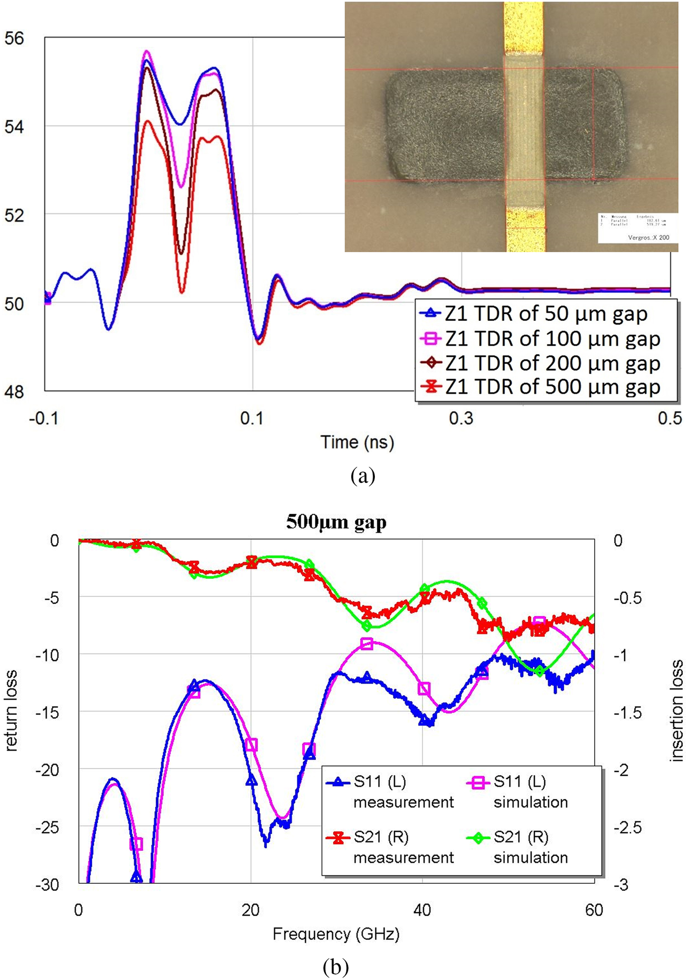
To determine the electrical properties of the gap filler material, gaps were lasered into the PCB with well-known electrical properties (same material as used in Fig. 8). These were filled with the gap filler material and afterward overprinted with AJ (Fig. 9). The impedance steps of different gap widths were then analyzed with a R&S ZVA 67 GHz network analyzer in the time domain. For the determination of the electrical properties, the largest investigated gap with 500 µm is most suitable since it requires the lowest spatial resolution. Since the impedance steps at a gap width of 200 µm are not very different from the impedance of the gap width of 500 µm, it can be assumed that the spatial resolution is high enough. To obtain an impedance of 50 Ω with the here printed line width of 215 µm, the necessary material parameters of the filling material can be determined by simulation (Fig. 9, bottom). Simulations with a dielectric constant (DK) of 4.2 and a dissipation factor (DF) of 0.016 for the gap filling material lead to best matching to the measurement results. The datasheet gives a value for DK of 4.72 (@ 1 kHz) and no value for DF.
Impedance steps of different gaps printed by AJ (top) and S-Parameter comparison of 500 µm gap (simulation and measurement, bottom).
Measured performance of AJ connection
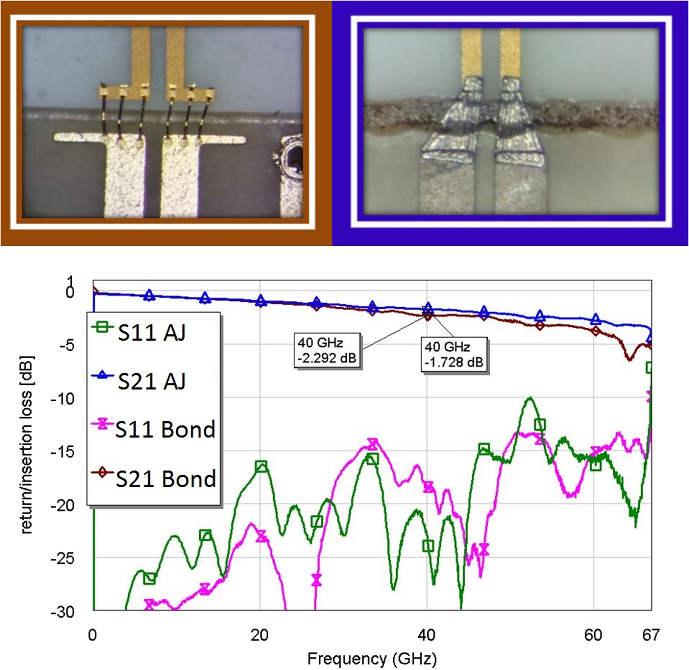
As chip carriers, the packages well-characterized in [Reference Roehrl, Jakob, Bogner, Hageneder and Zorn2] were used. The fabricated broadband differential structures allow an analysis of the aerosol transition from DC to 67 GHz. The measurement setup and the deembedding procedures used are identical to those in [Reference Roehrl, Jakob, Bogner, Hageneder and Zorn2].
Figure 10 shows the comparison of an AJ and a bond transition. The transition contains one connection from baseboard to package and from package to chip. As mentioned in [Reference Roehrl, Jakob, Bogner, Hageneder and Zorn2] the return loss is dominated by the transition from baseboard to package (which is still the same in both cases). The more important difference of both transition types can be seen in insertion loss. Because AJT allows silver as surface finish at the package, the insertion loss can be reduced by 0.56 dB (@40 GHz). This means a reduction of power losses of 6% absolute per transition. Moreover silver is cheaper than gold as surface finish.
Comparison of deembedded baseboard with chip transition.
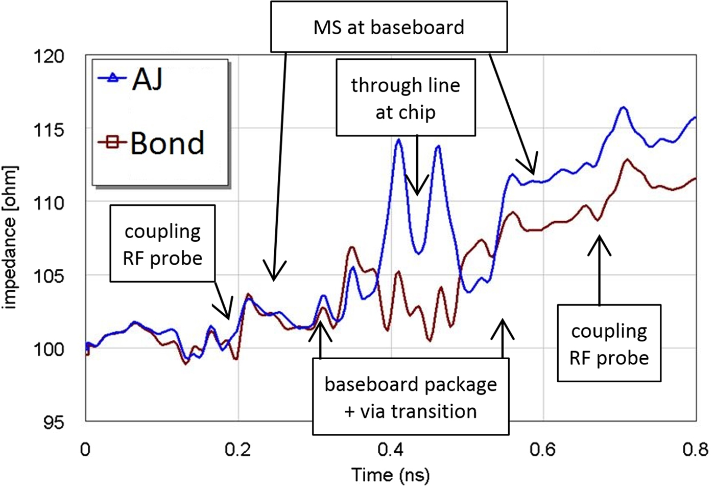
Time-domain reflectometer (TDR) measurements (Fig. 11) allow to review the quality of the designed and produced packages and transitions in detail. It shows the impedance of the whole measurement path between the coaxial calibrated connectors of the VNA (frequency range from 67 MHz to 67 GHz). In comparison with the bond transition, which is matched very well to the desired 100 Ω, the impedance of the AJ transitions is too high. This may be the main reason, why the return loss of the AJ package is not as good as the return loss of the bond package in Fig. 10. However, considering that the AJ junction has no compensation structures on both sides (the chip and the package, Fig. 10 top), the performance is very good. The bond transition would have been significantly worse without compensation.
TDR measurement of differential 0.65 mm BGA incl. baseboard and RF probes (measured with R&S ZVA 67).
Conclusion
Currently, well-established bonding technologies for interconnections are mechanically very flexible and can bridge large distances (even over other components) especially at lower frequencies. Furthermore, the two connection points may even have materials with significantly different coefficients of thermal expansion. However, it must be ensured that the surface finishes are bondable. Especially in the millimeter wave frequency range, AJ technology offers great advantages as compared with bond wires as, in principle, any two conductive surfaces can be interconnected. It has been shown, that this leads to a significant reduction in insertion loss. In addition, the line impedance of the interconnect can be designed as required, enabling low-loss, low-reflection broadband transitions up to the three-digit GHz range.
Acknowledgements
The Project InTeRaPID – “Interconnect Technologies for Radio Frequency PCB Integrated Devices” is financially supported by the Bavarian Research Foundation (AZ 1057-12). All kinds of support are gratefully acknowledged.
 Franz Xaver Röhrl received a degree in electrical engineering and information technology from the Technical University of Munich in 2013. He now does his doctorate in the field of PCB technology for millimeter wave applications. His main research interests are the design and optimization of high-frequency millimeter wave submounts.
 Johannes Jakob received his master of electrical engineering degree in 2011 from the Deggendorf Institute of Technology. He is currently serving as project engineer at the Institute for Precision Manufacturing and High-Frequency Technology and his main research interests are simulations and measurements of millimeter wave structures.
 Werner Bogner received his Diploma in Electrical Engineering in 1988 from Technical University Munich and his Dr.-Ing. degree also from TU Munich in 1994. Thereafter, he was working for Siemens AG and Infineon AG on several topics of high-frequency electronics. Since 2003 he is a professor at Deggendorf Institute of Technology with focus on circuitry and rf-electronics.
 Robert Weigel received the Dr.-Ing. and the Dr.-Ing.habil. degrees from the TU Munich, Germany. From 1996 to 2002, he was the Director of the Institute for Communications and Information Engineering, University of Linz, Austria, where, in August 1999, he co-founded the company DICE, which was then split into an Infineon Technologies (DICE) and an Intel (DMCE) company. Since 2002, he has been the Head of the Institute for Electronics Engineering at the University of Erlangen, Germany. He has published more than 900 papers in the fields microwaves, electronics, and communication. Dr. Weigel is an Elected Member of the German National Academy of Science and Engineering and an Elected Member of the Senate of the German Research Foundation. He was an IEEE Distinguished Microwave Lecturer and the 2014 MTT-S President. He is an IEEE Fellow and an ITG Fellow, and he received the 2002 VDE ITG-Award, the 2007 IEEE Microwave Applications Award, the 2016 IEEE Distinguished Microwave Educator Award, the 2018 IEEE Rudolph E. Henning Distinguished Mentoring Award and the 2018 EuMA Distinguished Service Award.
 Stefan Zorn received the Dipl.-Ing. degree in Electronics Engineering from the Friedrich-Alexander-University of Erlangen-Nuremberg in 2007. Subsequently, he received the Dr.-Ing. degree from the same University in 2012. His research field has been the precise localization of mobile phones in natural disaster scenarios. Since 2012 Dr. Zorn is working as head of R&D PCB Technology at company Rohde & Schwarz. In addition, he holds the chair of RF Engineering at the Deggendorf Institute of Technology since 2016.


 Open access

