


Introduction
The rapid growth of data-driven applications and advancements in telecommunication systems have heightened the demand for faster, more reliable networks, and high-power, high-frequency circuits beyond the W-band. In this context, Indium Phosphide (InP) plays a pivotal role with its exceptional electronic and optical properties, positioning it as a key enabler for cutting-edge 6 G communication systems. Its direct bandgap, high electron velocity, and favourable thermal characteristics make it ideal for high-frequency applications. In this context, InP-based Double Heterojunction Bipolar Transistors (DHBTs) stand out as one of the few technological platforms capable of meeting the performance requirements. More specifically, “Type-II” InP/GaAsSb DHBTs have shown high cut/off frequencies f T [Reference Shiratori, Hoshi and Matsuzaki1] and f MAX [Reference Arabhavi, Ciabattini, Hamzeloui, Flückiger, Saranovac, Han, Marti, Bonomo, Chaudary, Ostinelli and Bolognesi2], with breakdown voltage BV CEO > 4.5 V. The excellent small-signal performances of devices fabricated in “emitter-fin” technology were validated with measurements up to 330 GHz [Reference Arabhavi, Deng, Ciabattini, Hamzeloui, Saranovac, Chaudary, Ebrahimi, Ostinelli, Maneux and Bolognesi3]. Furthermore, W-band InP/GaAsSb DHBT power amplifiers (PAs), fabricated using standard (i.e. non-fin) technology, can achieve the highest measured power density > 10 mW/µm2 [Reference Hamzeloui, Arabhavi, Ciabattini, Flückiger, Marti, Ebrahimi, Ostinelli and Bolognesi4] and a record class-A Power-Added-Efficiency (PAE) = 37.8% [Reference Hamzeloui, Arabhavi, Ciabattini, Ebrahimi, Müller, Ostinelli, Schröter and Bolognesi5]. The outstanding performances observed in W-band demand for further characterization at even higher frequency ranges to explore their capabilities.
Load-pull large-signal measurements at frequencies beyond the W-band are both challenging and rare [Reference De Martino, Galatro, Romano, Parisi and Spirito6], yet they are essential for the comprehensive characterization of PAs or PA cells designed for operation in higher frequency bands. Load-pull measurements help identifying the optimal load impedance to achieve the maximum gain, output power and efficiency, which is critical for designing PAs. They are also fundamental for the validation of large-signal models. The insights provided by a load-pull characterization are crucial to capture the non-linearity of the device when it approaches the gain compression region.
In the present work, we report two different (0.25 × 10) µm2 single-finger common-emitter DHBTs with different collector epitaxial design that show excellent small-signal and load-pull large-signal performances in G-band (140 to 170 GHz). We will present the differences between the two epitaxial designs, highlighting the effect that they cause on the small-signal performances at different biases, while maintaining a cut-off frequency f MAX > 1 THz. Then, a complete load-pull characterization will be provided, followed by a thermal characterization of the epitaxial designs. The reported values of P OUT,SAT > 10 dBm and PAE > 30% for both epitaxial designs over the whole frequency range, PAE = 39.2% at 140 GHz and 38.6% at 170 GHz represent the highest ever reported in G-band in any technology. This confirms the excellent capabilities of InP/GaAsSb DHBTs as a prime technology for the next generation of high-speed communications.
An earlier version of this paper was presented at the EuMIC 2024 and was published in its Proceedings [Reference Ciabattini, Hamzeloui, Arabhavi, Ebrahimi, Ostinelli and Bolognesi7].
Device description
Epitaxial layers
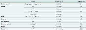
The two DHBT epitaxial layers were grown by metal-organic chemical vapour deposition (MOCVD) on 2-inch semi-insulating substrates. The two only differ for the sub-collector design: the first one features a 50 nm of heavily doped InP and 20 nm of lattice-matched GaInAs, which operates as the collector contact layer, whereas in the second one the InP is completely omitted and the GaInAs layer is thinned to 7.5 nm and made In-rich. The thermal conductivity of the GaInAs is lower when it is lattice-matched on InP, but increases for both Ga-rich and In-rich [Reference Adachi8]. In-rich composition has a higher electron mobility, which helps compensating for the increase in sheet resistance of the thinner layer [Reference Chattopadhyay, Sutradhar and Nag9]. The fraction of Indium in the layer was set to 62%, due to limits in the MOCVD growth.
The details of the two structures are reported in Tables 1 and 2. From now on, they will be labelled structure A for the thicker sub-collector and B for the thinner one.
Epitaxial structure A

Epitaxial structure B

Device fabrication
The fabrication process begins with the pattering in e-beam lithography of the emitter contact, followed by a metal deposition with an e-beam evaporator. The emitter mesa is partially etched and the “emitter-fin” of the emitter cathode is patterned and deposited. This addition to the emitter metal sets the distance between the emitter mesa side-wall and the yet to be deposited base metal, also called “base-access-distance”. At the same time, it also allows for the deposition of a thicker base metal. These two effects combined dramatically decrease the base resistance, thus boosting the RF-performances of the DHBT [Reference Arabhavi, Ciabattini, Hamzeloui, Flückiger, Saranovac, Han, Marti, Bonomo, Chaudary, Ostinelli and Bolognesi2].
Next, the emitter mesa etching is completed and the base metal deposited in a self-aligned fashion over the emitter metal. Then, the emitter mesa side-wall and the base-access-distance are passivated with aluminum oxide (AlOx). The base-collector mesa is etched and the collector contact deposited. The devices are isolated one from the other and planarized with Teflon Amorphous Fluoropolymer (TAF). GSG probing pads conclude the fabrication. Besides different etching times for the collector, there is no difference in the fabrication process of the transistors based on the two epitaxial structures. Details of the fabrication process can be found in [Reference Arabhavi, Ciabattini, Hamzeloui, Flückiger, Saranovac, Han, Marti, Bonomo, Chaudary, Ostinelli and Bolognesi2, Reference Bolognesi, Arabhavi, Hamzeloui and Fornari10]. Figure 1a and 1b show the FIB/SEM cross-section of the final transistors with the epitaxial structure A and B, respectively.
FIB/SEM cross-section of the (0.25 × 10) µm2 DHBT fabricated on the epitaxial structure A (a) and B (b). In (b) it can be seen how the separation between the base and the collector contacts is smaller, as highlighted by the arrows.

DC and RF measurements
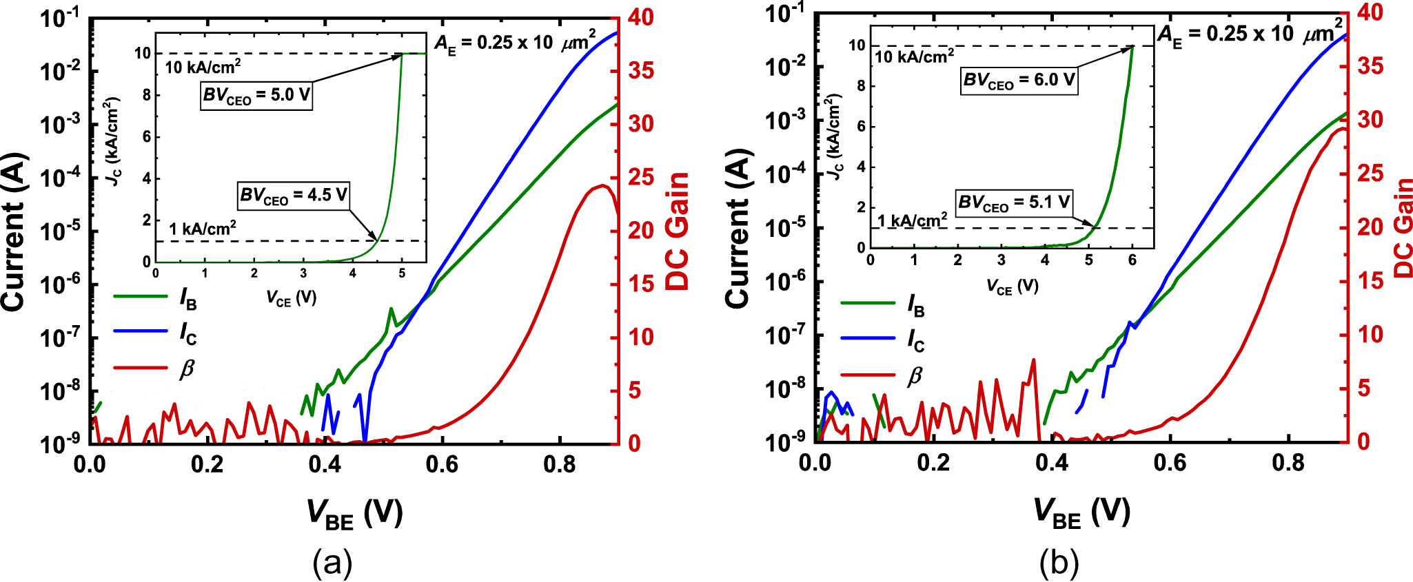
Figure 2 reports the DC Gummel characteristics of a (0.25 × 10 µm2) single-finger common-emitter DHBT, with the open-base common-emitter breakdown voltage characteristics displayed in the insets for both epitaxial structures A and B. They both feature a DC gain β ≥ 25 and a BV CEO ≥ 4.5 V. This confirms the excellent voltage-handling capabilities of this technology.
Typical gummel characteristics of (0.25 × 10) µm2 DHBT at V CB = 0 v fabricated on the epitaxial structure A (a) and B (b). (Inset) measured breakdown characteristics, with BV CEO reported at both 1 ka/cm2 and 10 ka/cm2.

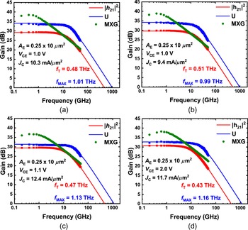
The small-signal performances of the transistors were measured from 0.2 to 50 GHz. Figure 3 shows |h 21|2, U, MAG/MSG and the corresponding cut-off frequencies f T/f MAX for the epitaxial structures A and B at (a), (b) peak f T bias point and (c), (d) peak f MAX.
RF characteristics of a (0.25 × 10) µm2 DHBT. |h21|2, U and MAG/MSG are reported for (a) and (b) best f T bias condition and (c) and (d) best f MAX bias condition for the epitaxial structure A (a)–(c) and B (b)–(d).

The epitaxial structure A shows f T = 0.48 THz at V CE = 1.0 V, J C = 10.3 mA/µm2 and f MAX = 1.13 THz at V CE = 1.1 V, J C = 12.4 mA/µm2. The epitaxial structure B shows f T = 0.51 THz at V CE = 1.0 V, J C = 9.4 mA/µm2 and f MAX = 1.16 THz at V CE = 2.0 V, J C = 11.7 mA/µm2.
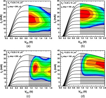
Both structures have excellent small-signal performances, but to better understand their dependence on the applied bias, it is useful to look at the evolution of the cutoff frequencies f T/f MAX over different biases. Figure 4 shows the I-V curves of a (0.25 × 10) µm2 DHBT with f T and f MAX superposed on them for the epitaxial structure A (Fig. 4a and 4c) and B (Fig. 4b and 4d). It is clear how for the epitaxial structure B the range of high small-signal performance is extended both in I C and V CE with respect to the structure A. This feature is highly attractive for a PA design, as it gives great flexibility in the PA cell biasing. Having such high and stable cut-off frequencies enables to reach very high P OUT and PAE without compromising on small-signal RF performances.
Contours showing the variation of f t (a)–(b) and f max (c)–(d) with bias superposed over the I-V curves of a (0.25 × 10) µm2 DHBT for the epitaxial structure A (a)–(c) and B (b)–(d). Each colour contour corresponds to a 2.5% reduction from peak f t and f max.

Large-signal load-pull measurements
In order to investigate the power performances of InP/GaAsSb DHBTs and to properly highlight the differences between the epitaxial structures A and B, the devices were characterized at Vertigo Technologies, by means of an active vector-modulation solution [Reference De Martino, Galatro, Romano, Parisi and Spirito6].
The bias choice is of paramount importance in large-signal measurements, as it affects dramatically figures of merit such as P OUT, G OP and PAE. Transistors used in PAs are usually biased in different conditions than those at which they reach their best small-signal performance. In order to achieve class-A operation, we used a collector current density of J C = 8.0 mA/µm2, around 70% of the density of current needed for peak f MAX, and half of the value J MAX for which there is the onset of thermal effects in the I-V curves. This value of J C allows an active load line without the risk of current-clipping.
The transistors of both epitaxial structures were measured with the collector-emitter voltage starting from V CE = 1.2 V and increased until degradation. For structure A, the degradation happened after V CE = 1.8 V, whereas for B after V CE = 2.0 V. From now on, we will only focus on the results for these bias points.
The load-pull measurements were done at four frequencies, 140, 150, 160 and 170 GHz. First, the optimal load for different input power P IN was found. Figure 5 shows the measured P OUT and PAE contours at 140 and 170 GHz for the epitaxial structure A (Fig. 5a and 5b) and B (Fig. 5c and 5d). For the structure A, the contours do not fully close at 140 GHz, but they do at 170 GHz. For both structures, P OUT and PAE contours do not coincide, yet they show a good overlap. Loading a transistor close to the optimum load for both P OUT and PAE is a desirable feature, because it allows a good compromise between output power and efficiency. It is also clear that the optimum load Z L for both structures at both 140 GHz and 170 GHz is close to the centre of the Smith chart. This is an appealing feature when designing a power amplifier, because the output impedance of the transistor requires a low impedance transformation ratio to a 50 Ω system, a valuable quality in application requiring a low-loss broadband impedance match.
Load-pull contours at P IN,SAT for P OUT (blue) and PAE (red) of a (0.25 × 10) µm2 DHBT for the epitaxial structure A (a)–(b) and B (c)–(d) at V CE = 1.8 V, J C = 8.0 ma/µm2 for a and V CE = 2.0 V, J C = 8.0 ma/µm2 for B. The contours reflect measurements done at 140 ghz in (a) and (c) and 170 ghz in (b) and (d).

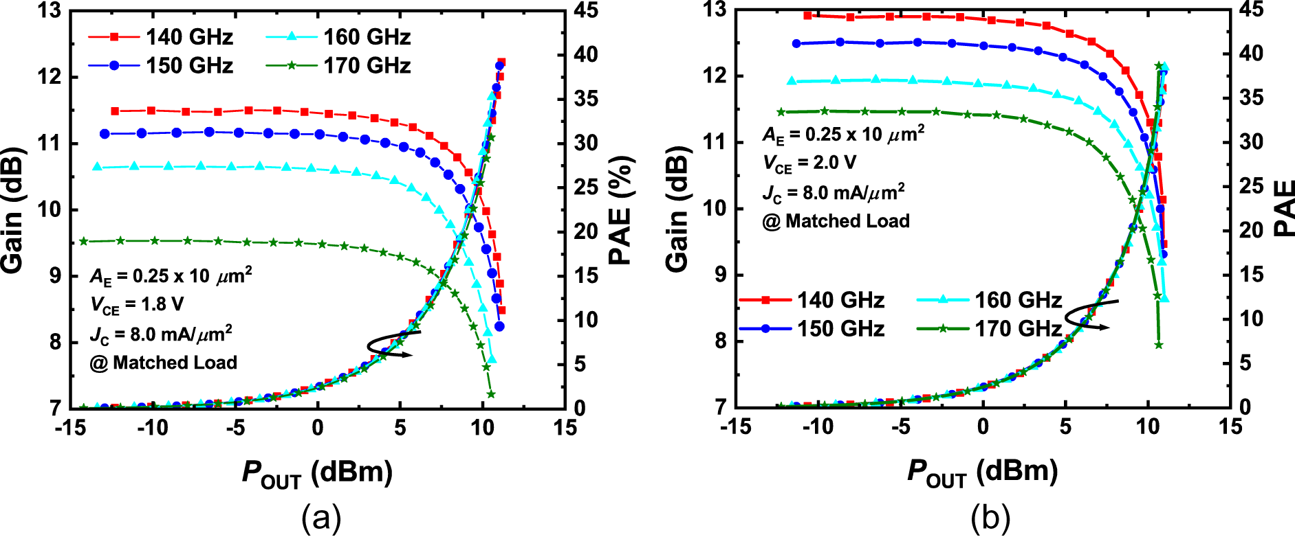
After performing the load-pull measurements, power sweeps were carried out with optimum load impedance Z L,OPT to determine the highest P OUT and PAE. Figure 6 reports the operational gain G OP and PAE against the output power P OUT between 140 and 170 GHz, in steps of 10 GHz, for the epitaxial structure A (a) and B (b), respectively, for a (0.25 × 10) µm2 DHBT.
Gain and PAE versus P OUT at different frequencies of a (0.25 × 10) µm2 DHBT for the epitaxial structure A (a) and B (b). The load is matched for maximum output power.

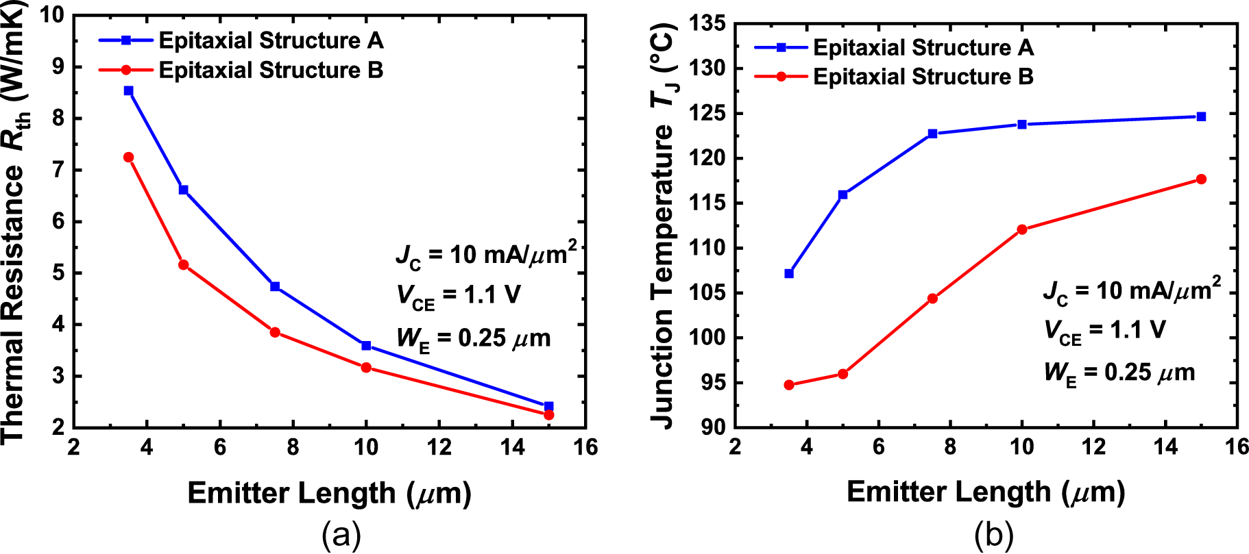
Thermal resistance R TH (a) and junction temperature T J (b) for the epitaxial structures A (blue) and B (red) measured at V CE = 1.1 V and J C = 10 mA/µm2.

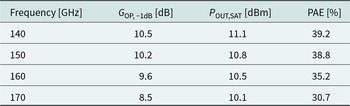
The two structures exhibit quite different behaviours. By increasing the frequency, the transistor realized with the epitaxial structure A shows decreasing G OP, PAE and P OUT. Instead, the transistor realized with the structure B exhibits decreasing gain, but almost unchanged PAE and P OUT. The results are summarized in Tables 3 and 4.
Measured gain at –1 dB compression, output power at –3 dB compression and PAE at different frequencies for the epitaxial structure A

Measured gain at –1 dB compression, output power at –3 dB compression and PAE at different frequencies for the epitaxial structure B

Epitaxial structure B shows a higher gain, due to the superior small-signal gain at the bias point for which the best large-signal performances are observed, as reported in Fig. 4c and 4d.
Both structures offer good saturated output power and very high efficiency. This demonstrates the excellent power performance of Type-II InP-DHBTs. To the best of the authors’ knowledge, these results represent a record in terms of PAE for the entire G-band.
Thermal characterization
In order to further characterize and understand the differences between the two epitaxial structures and thus, the effect that a thinner subcollector has on the performances of a InP-DHBT, the transistors were thermally characterized. It was reported [Reference Ciabattini, Arabhavi, Hamzeloui, Ebrahimi, Ostinelli and Bolognesi11–Reference Grandchamp, Nodjiadjim, Zaknoune, Koné, Hainaut, Godin, Riet, Zimmer and Maneux14] how engineering the emitter and collector epitaxial layers can offer significant advantages to the thermal resistance of a bipolar transistor.
In a DHBT, the majority of the heat is generated in the collector. The thermal conductivity of InP and GaInAs, if lattice matched to InP, is κ = 68 W/mK and κ = 5 W/mK, respectively. Thus, the removal of the 50 nm thick InP and the thinning of the GaInAs layer for the epitaxial structure B, is expected to bring great benefits to the transistor performance.
The thermal resistance R TH is a metric of self-heating in a DHBT. When high, it indicates that the generated heat is not properly shunted, which then leads to an increased junction temperature T J. An elevated T J causes an earlier degradation of the device performances.
In any bipolar transistor a rise in T J leads to a reduction of the base-emitter voltage V BE required to achieve a given current density J C. The thermal-electric feedback coefficient Φ takes this effect into account, and is defined as [Reference Liu, Chau and Beam15, Reference Müller, d’Alessandro, Falk, Weimer, Jin, Krattenmacher, Kuthe, Claus and Schröter16]:
 \begin{equation}\Phi {\left. { = - \frac{{\partial {V_{{\text{BE}}}}}}{{\partial T}}} \right|_{({I_C} = {\text{const}})}}\end{equation}
This coefficient is obtained from Gummel plots measured at different temperatures. Then, it can be used to calculate the thermal resistance R TH of the device as:
 \begin{equation}{R_{{\text{TH}}}} = \,\frac{{{\Delta}{V_{\text{BE}}}}}{{{\Delta}{V_{{\text{CE}}}} \cdot {I_{\text{C}}} \cdot \Phi }}\end{equation}
where ΔV BE is the voltage difference in the base-emitter voltage for a fixed collector current I C when the collector-emitter voltage is changed by a fixed amount ΔV CE. After R TH is calculated, the junction temperature T J can be derived by using:
 \begin{equation}\,\,\,\,\,\,{T_{\text{J}}} = {T_{\text{A}}} + {R_{{\text{TH}}}} \cdot {V_{{\text{CE}}}} \cdot {I_{\text{C}}}\end{equation}
where T A is the ambient temperature. Figure 7 shows the results of the extracted thermal resistance and the calculated junction temperature of both epitaxial structures for different emitter lengths and for an emitter width W E = 0.25 µm. The results are reported for V CE = 1.1 V and J C = 10 mA/µm2.
The epitaxial structure B shows, for the emitter length L E = 10 µm, an improvement of more than 10% in thermal resistance, compared with the structure A and a similar reduction in junction temperature. These results are in agreement with what was reported in [Reference Ciabattini, Arabhavi, Hamzeloui, Ebrahimi, Ostinelli and Bolognesi11].
Conclusion
In this work, we reported a detailed small-, large-signal and thermal analysis of two different (0.25 × 10) µm2 single-finger common-emitter InP/GaAsSb DHBTs, both fabricated in “emitter-fin” technology, but with different collector designs.
Both designs exhibit f T close or above 500 GHz and THz-class f MAX over a wide range of bias points, especially for the optimized collector design. The load-pull large-signal characterization shows very good power-handling capabilities together with outstanding efficiency, with an optimum load impedance Z L,OPT close to the centre of the Smith chart. The PAE reported in this work represents a record in the whole G-band for any technology, reaching 39.2 % at 140 GHz and 38.6 % at 170 GHz.
Finally, it was demonstrated how a wise design of the subcollector layer reduces the thermal resistance of the transistor, broadening the biasing range to achieve close-to-peak small-signal performance and delaying the degradation during large-signal measurements. This work further demonstrates the potential of emitter-fin InP/GaAsSb DHBTs for highly-efficient high-power PAs at G-band and above.
Acknowledgement
The authors thank the staff of FIRST Lab at ETH Zurich, Zurich, Switzerland for their support with the fabrication and Vertigo Technologies and TU Delft, Delft, Netherlands for their support with the load-pull measurements.
Competing interests
The authors declare none.

Filippo Ciabattini was born in Fiesole (Italy) on September 27, 1993. In 2015 he received his Bachelor degree in Physical Engineering at Polytechnic of Turin (Italy) and in 2017 his M.S. in Nanotechnologies for ICTs, a joint Master among Polytechnic of Turin, INP Grenoble (France) and EPFL (Switzerland). Then he joined the University of Hamburg, working on opto-nanofluidic devices. In October 2019 he started his PhD in the Millimeter-Wave Electronics Group at ETH Zürich. His main research area is the design, process development, fabrication and characterization of InP/GaAsSb based Double Heterojunction Bipolar Transistor (DHBTs).

Sara Hamzeloui is a Ph.D. student at Millimeter-Wave Electronics (MWE) Group at ETH Zurich under the supervision of Prof. Colombo Bolognesi. She received her B.Sc. and M.Sc. from the Sharif University of Technology in Tehran, Iran, in 2016 and 2018, respectively. She is currently working on the design, fabrication, and characterization of high-power InP/GaAsSb DHBT device and circuit technology for mm- and sub-mm-wave power amplifiers.

Akshay Mahadev Arabhavi is a postdoctoral researcher at Millimeter-Wave Electronics Laboratory, ETH Zurich. He received his Ph.D. from ETH Zurich and M.Sc. in Microelectronics jointly from NTU-Singapore and TU Munich. His research focuses on developing next generation high-frequency semiconductor devices and circuits on the Indium Phosphide platform for mmWave and THz technologies.

Mojtaba Ebrahimi Maroufi was born in Tabriz, Iran on November 28st, 1996. He received his B.Sc. and M.Sc. degrees in Electrical Engineering from Sharif University of Technology, Tehran in 2019 and 2021 respectively. After the completion of his studies, Mojtaba joined Millimeter-Wave Electronics (MWE) Group as a Ph.D. candidate under the supervision of Prof. Dr. Colombo Bolognesi at the Swiss Federal Institute of Technology (ETH Zürich). His main research interests include mm-wave circuit design and InP/GaAsSb based Double Heterojunction Bipolar Transistor (DHBTs) fabrication.

Olivier Ostinelli was born in Lugano, Switzerland. He received the Ph.D. degree from the Swiss Federal Institute of Technology (ETH Zürich), Zürich, Switzerland, in 2006. In 2006, he joined the Millimeter-Wave Electronics Group, ETH Zürich. His research work is focused on the crystal growth of InP-based double heterojunction bipolar transitors (DHBTs), high electron mobility transistors (HEMTs) and uni-travelling-carrier photodiodes (UTC-PDs).

Colombo R. Bolognesi earned the B.Eng. from McGill University, the M.Eng. from Carleton University, and the Ph.D. from UCSB. In 1994, he joined Northern Telecom as a BiCMOS Process Integration Engineer for high-speed submicron polysilicon emitter BJTs. He joined the Engineering Science and Physics Departments at Simon Fraser University in 1995 to launch and direct SFU’s Compound Semiconductor Device Fabrication Laboratory (CSDL) where he pioneered the InP/GaAsSb heterojunction system for DHBTs. In 2001, his team demonstrated the first bipolar transistors with f T/f MAX cutoff frequencies exceeding 300 GHz with a 6V breakdown.
In 2006, he took the Chair of Millimeter-Wave Electronics at ETH-Zürich. His Group demonstrated THz DHBTs, 300 Gbps GaInAsSb/InP UTC-PDs, the first 200 GHz GaN HEMTs, and developed ultralow-noise InP HEMTs used in European Space Agency (ESA) Deep Space Network ground station cryogenic amplifiers for deep space missions around Mars, Jupiter, Mercury, and dark matter mapping.


 Open access