


Introduction
One common approach for increasing the capacity of today's wireless communication systems is the employment of higher order modulation schemes along with more and more efficient channel coding schemes. With these approaches, data rates in the order of several tens of Gbit/s can be expected in the upcoming wireless standards. However, for some applications that are rather located in the back-end of a communication system, the increased design complexity that comes along with the mentioned techniques is adverse regarding the deployment of large numbers of communication links at a reasonable cost. One example of the above are wireless high-data-rate links for data transfer inside of devices, e.g. for the transmission of uncompressed ultra-high resolution video. Terahertz (THz) data links, which build upon the exploitation of huge portions of spectrum, are a promising candidate to realize such kind of flexible wireless data links at the boundary condition of low-system complexity. The THz intra-device communication channel is constituted by the materials and geometry of the device casing as well as the presence of the electronic building parts throughout the surfaces of the implemented printed circuit boards (PCBs). So far, there have been studies on the impact of flat ground planes made of metals [Reference Fettweis, ul Hassan, Landau and Fischer1] and plastic materials [Reference Fricke, Rey, Achir, Le Bars, Kleine-Ostmann and Kürner2]. Furthermore, the impact of larger structures along the propagation part on a single board such as heat sinks or memory modules has been investigated in [Reference Kim and Zaji3]. In this publication, the so-far unconsidered influence of structures in the order of a single wavelength especially on board-to-board communications is treated. A model for reflection processes at PCB surfaces is derived from vector network analyzer (VNA) measurements with the aim to facilitate ray-tracing-based propagation simulations for intra-device communications in the THz frequency range.
In the remainder of the paper, the section “Measurement setup and methodology” introduces the measurement setup and methodology. Subsequently, in the section “PCB scattering model”, the scattering model for simulating the observed reflection behavior is developed. The section “Simulated annealing algorithm” describes the implementation of a simulated annealing algorithm for optimizing the model behavior to match the measurement results. The model is then modified to allow its utilization for propagation simulation in realistic scenarios in the section “Adoption to realistic propagation environments” Finally, in the section “Model and calibration analysis and discussion” the performance of the model is analyzed and discussed before the conclusions are drawn, and an outlook is provided in the section “Conclusion”.
Measurement setup methodology
The measurements have been performed with a Rohde & Schwarz ZVA50 VNA along with ZVA-Z325 frequency extensions. The frequency extensions have been equipped with two identical 20 dBi standard gain horns manufactured by Flann Microwave. The measurement bandwidth was set to 100 kHz and the system has been calibrated with the waveguide flanges of the frequency extensions as a reference plane. The mechanical setup for performing the angle-dependent reflection measurements of the S21-parameter consisted of a two-arm goniometer capable of rotating the frequency extensions around the PCB. The experiment geometry is depicted schematically in Fig. 1. The measurements have been performed in perpendicular linear polarization with 3201 points in the frequency range between 270 and 320 GHz. The PCB used for the measurements has been taken from an LCD beamer which is considered as an example of a typical piece of audiovisual / multimedia equipment. The five spots shown in Fig. 2 , which are located at different places of the PCB front- and backside, have been measured to generate a number of measurement samples with varying compositions of surface components and details.
Experiment geometry.

Measured positions on the front- (top) and back-side (bottom) of the PCB.

PCB scattering model
The modeling methodology of the PCB reflection behavior is based on the assumption of a superposition of multiple diffuse reflection processes on the PCB surface. Moreover, the approach has been developed with the implementation to a frequency-domain ray-tracing algorithm in mind. The input to the model are the coordinates of the transmitter (Tx) and receiver (Rx) positions along with the point of specular reflection of the considered propagation path. The model output is a set of reflected field components, each consisting of an amplitude coefficient, a frequency-dependent phase angle with respect to the path delay and the angular coordinates in azimuth and elevation relative to the propagation path generated by the ray-tracing algorithm. This way, it is possible to apply arbitrary antenna radiation patterns in a post-processing step. The geometry of a reflection process illustrating the following considerations is shown in Fig. 3. Following the theory of geometrical optics, the electromagnetic wave from transmitter to receiver is assumed to be a locally plane wave, propagating along straight ray paths through free space. The specular reflection path generated by the underlying ray-tracing algorithm is depicted red in the figure above. Thinking of the Tx as a point-source, this leads to a globally spherical wave-front, eventually reaching the surface features of the PCB with different time delays depending on the actual position. It is further assumed that the major contribution of the reflected field is generated within an area around the point of specular reflection called the active scattering region (ASR). The calculation of the ASR geometry is based on the intersection of the reflection plane with an ellipsoid surrounding the Tx and an orthogonal projection of the Rx through the reflection plane as derived in [Reference Klein4]. Inside the ASR, a number of diffuse reflection processes lead to a superposition of reflected field components that summarize at the receiver, forming the received signal. The model is characterized by the four parameters sasr, dd, rdiff, and hb, the values of which have been determined by simulated annealing as described in the section “Simulated annealing algorithm”. The values are implicitly holding the surface properties and are expected to provide different value sets for different types of PCBs. Figure 4 illustrates the distribution of reflection processes in the vicinity of the specular reflection path. Figure (a) introduces the geometrical measures for the angle of reflection Θ, the local polar coordinates of a diffuse reflection process with radius r, and angle ϕ and the radius of the ASR in a certain direction reff. The distances a and b in Fig. 4(b) depict the semimajor and semiminor axes of the ASR, respectively. The first model parameter sasr is the scaling factor of the area in which significant reflection processes are assumed to occur. It describes the curvature of the ellipsoid defining the ASR by the relation
 $$s_{asr} = \displaystyle{R \over D},$$
with D being the total distance between Tx and Rx projection and R being the maximum diameter of the ellipsoid. As illustrated in Fig. 4(b), a smaller value of sasr leads to a shortening of the semi-axes from a to a′ and b to b′. Inside the defined region, a number of reflection processes are generated and arranged in a rectangular grid. The grid fills the entire shape of the elliptical scattering region. The horizontal and vertical spacing between the grid lines and columns is defined by the model parameter dd, which corresponds to the number of scattering processes per mm. Based on these positions, the phases of the scattered signal components can be derived geometrically.
Geometry of the PCB reflection model.

ASR and reflection processes. (a) Coordinate System of the ASR. (b) Distribution of Reflection Processes.

The all-over reflectivity of the PCB is defined by the parameter rdiff. It represents the global reflection coefficient that is applied to every scattering process. Additionally, the amplitude is modified by a non-uniform amplitude distribution depending on the position of the reflection process inside the ASR, with a decreasing value with increasing distance from the specular reflection spot.
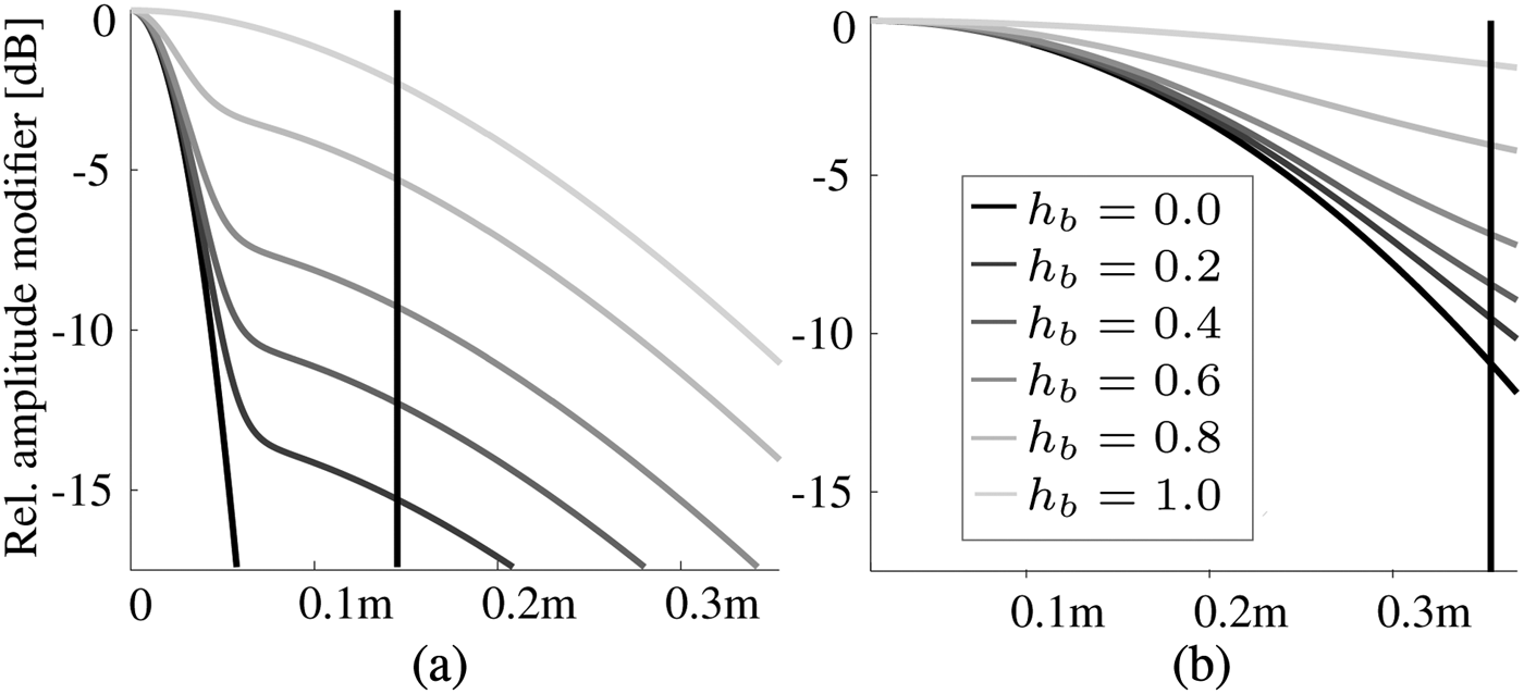
The amplitude distribution has its maximum in the center of the scattering region and its minimum at the borders of the region. The value at the borders as well as the transition between the maximum and the minimum are controlled by the shape parameter hb. As shown in Fig. 5, the relative amplitude distribution is furthermore depending on the angle of incidence (AoI). The vertical black line depicts the absolute stretch of the ASR. As seen in Figure (b), it is much larger for a larger AoI θ. In addition, the amplitude distribution is smeared out to the border of the ASR much more than in the case of a steeper incidence as shown in Figure (a). This behavior represents the fact that building parts further away from the specular point will have a stronger influence at large reflection angles due to their actual height. The value of the introduced amplitude modifier is calculated according to
 $$a_1 = \exp \left( { - \displaystyle{1 \over 2}{\left( {\displaystyle{{log(1 + r)} \over {r_{eff}}}} \right)}^2} \right){\rm },$$
 $$a_2 = \exp \left( { - \displaystyle{1 \over 2}{\left( {\displaystyle{r \over {r_{eff}}}} \right)}^2} \right){\rm },$$
 $$a_3 = ((1 - h_b) \cdot a_1 + h_b \cdot a_2)^{0.575},$$
with
 $$r_{eff} = \displaystyle{{a \cdot b} \over {\sqrt {a^2{\sin }^2\varphi + b^2cos^2\varphi } }}{\rm },$$
being the angle-dependent radius of the ASR and r being the distance between the actual scattering point and the specular reflection. The total amplitude of the generated scattering process results to
 $$a = r_{diff} \cdot a_3 \cdot \displaystyle{b \over a}$$
The factor b/a scales the amplitudes inversely proportional to the sine of the AoI θ as it has been observed that the model produces too large numbers of scattering processes resulting in an unrealistically high-total amplitude of the resulting signal otherwise. The phases of the scattering processes with respect to the specular reflection path are calculated based on the path difference between the specular reflection path and the scattered paths according to
 $$\phi = \exp \left( { - 2\pi if \cdot \displaystyle{\Delta \over {c_0}}} \right){\rm },$$
with Δ being the path difference to the specular path and c 0 being the speed of light.
Relative amplitude modifier over radius along the semi-major axis. (a) Angle of incidence 45°. (b) Angle of incidence 75°.
Simulated annealing algorithm
In order to extract the values of the model parameters from the measurements, a simulated annealing algorithm has been implemented [Reference Ingber5]. A flow chart of the algorithm is depicted in Fig. 6. To start with, an initial simulation result is generated. Based on this, the optimization process is controlled by two nested loops. The outer loop decreases the system temperature and correspondingly the acceptance probability of inferior simulation solutions according to the Metropolis Criterion [Reference Metropolis, Rosenbluth, Marshall, Teller and Teller6]. The inner loop generates a new simulation result with a single varied parameter which may or may not be accepted; upon acceptance or after a maximum of three repetitions at constant system temperature have been rejected, control is passed back to the outer loop and the temperature is further decreased. The optimization reaches its end when the threshold temperature is reached. The value ranges of the four model parameters along with their initial values in the beginning of the optimization process are summarized in Table 1. The initial temperature has been chosen as T 0 = 1000 with a cooling rate of rc = 0.003. In the beginning of the optimization, the initial simulation result R 0 is generated with the chosen starting parameter values. Each simulation result comprises a ray-tracing simulation of the measurement situation for four different angles of incidence AoI ∈ {45°, 55°, 65°, 75° }.
Flow-chart of the simulated annealing algorithm.

Value ranges and starting values of the parameters under optimization

For assessing the performance of a simulation run, both the ray-tracing and the measurement results are filtered and transformed to the time domain via inverse Fast Fourier Transform (iFFT) to obtain the respective channel impulse responses (CIRs). The filter function applied to the measurement and simulation results in the frequency domain is
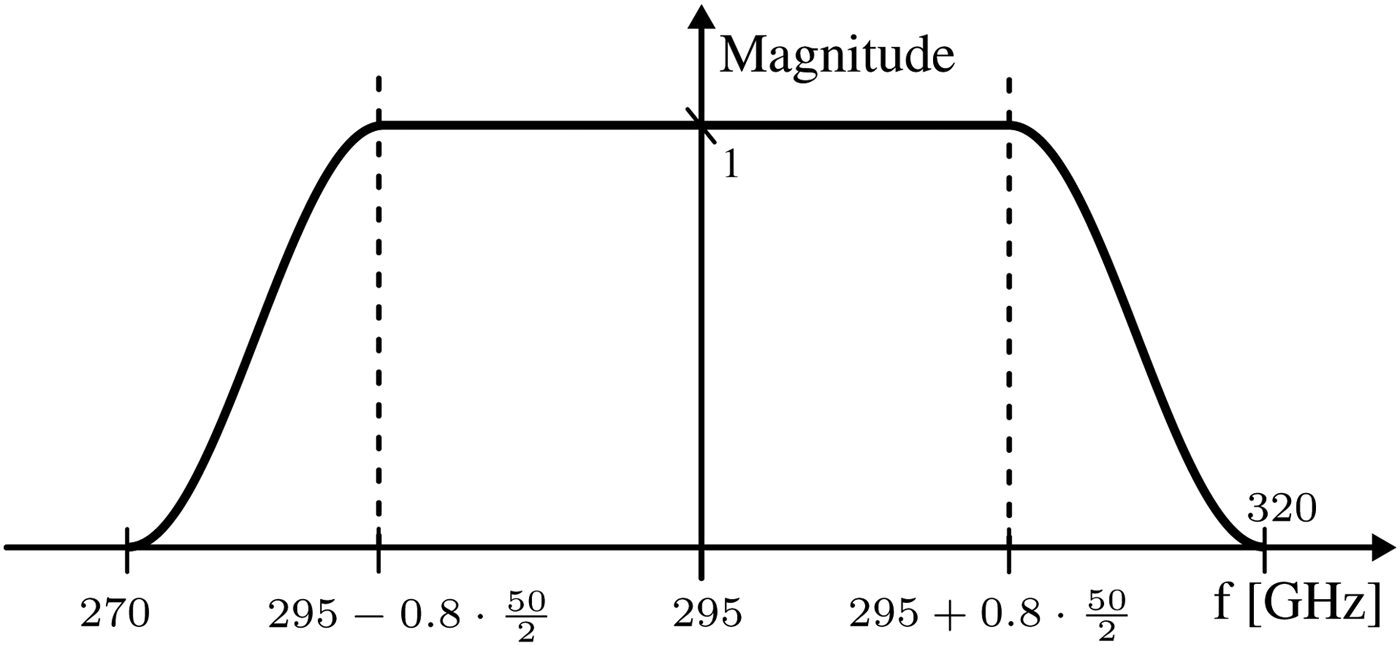
 $$M = cos^2\left( {\displaystyle{\pi \over {0.2 \cdot 50}}\left( {\vert f\,[GHz] - 295 \vert - \displaystyle{{0.8 \cdot 50} \over 2}} \right)} \right)$$
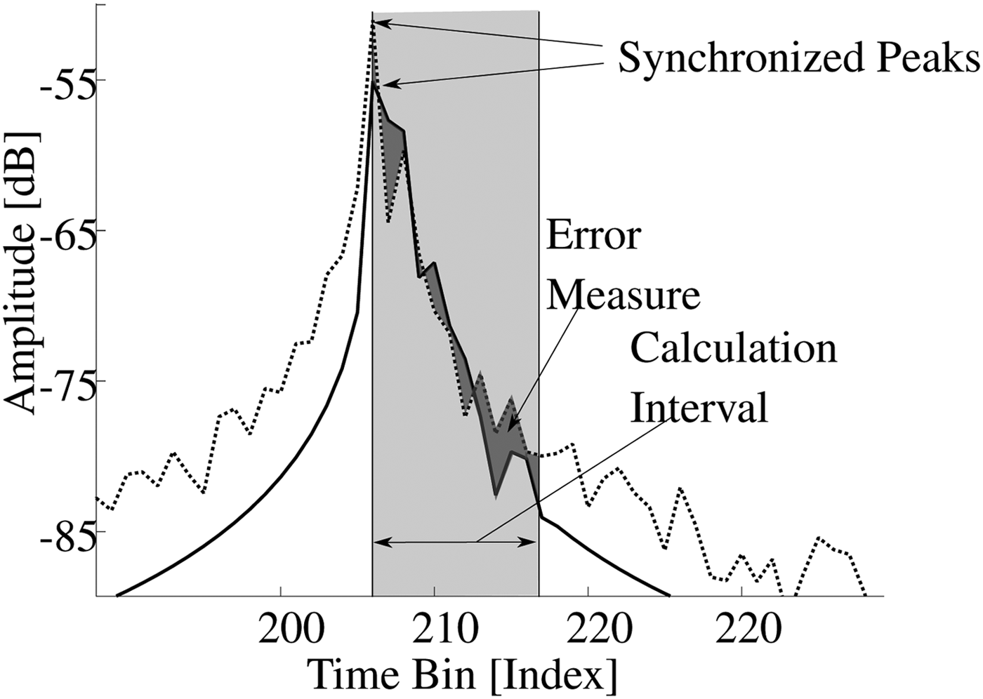
As shown in Fig. 7, it has a constant magnitude of 1 within 80% of the considered bandwidth while the lower and upper ends of the spectrum are masked out via a squared cosine function of frequency. This way, unwanted pulse broadening from iFFT leakage due to the non-periodicity of the spectra is suppressed. Each ray-tracing result is shifted such that the amplitude maxima of the simulation run and the corresponding measurement fall into the same time-domain bin. The cost measure C 0 of the initial solution is then calculated according to the cost function 9, i.e. the logarithmic difference between the simulation and measurement values of the peak i=1 and the following 11-time domain taps i=2, …, 11 is summarized for all angles of incidence and normalized by the number of considered angles.
 $$C_i = {\mkern 1mu} \displaystyle{1 \over 4}\sum\limits_{\scriptstyle a{\kern 1pt} \in {\kern 1pt} 45^\circ ,{\kern 1pt} 55^\circ , \atop {\scriptstyle 65^\circ ,{\kern 1pt} 75^\circ ; \atop \scriptstyle i = 1,...,12}} {\vert(} S_{a,i} - M_{a,i})\vert.$$
Thus, the performance measure is proportional to the mean area between simulation and measurement in the defined range of 12 bins, as further illustrated in Fig. 8. As long as the system temperature TSystem exceeds the defined threshold of Tmin = 0.5, another simulation run n is performed. Solutions providing a lower cost measure than the current optimum are always accepted while higher cost solutions are only accepted with a limited probability pacc which is decreasing with system temperature:
 $$p_{acc} = e^{\displaystyle{{C_{Optimum} - C_i} \over {T_{System}}}}.$$
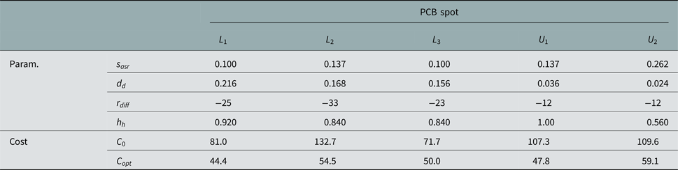
The algorithm has been executed for every measurement spot of the PCB, leading to the five sets of parameter values summarized in Table 2. In addition, the table compares the evolution of the cost function before and after optimization. Please note that the parameter values determined during optimization are different to those presented in [Reference Fricke, Achir, Le Bars and Kürner7] due to the fact that an additional filtering has been applied to the channel transfer functions as described above.
Window function applied to the measured and simulated CTFs.
Error measure defining the cost function.
Parameter values determined by simulated annealing
Model and calibration analysis and discussion
When representing a phenomenon or process with a model, an interesting question is the meaningfulness of the model parameters with respect to the underlying physical background. Having a look at the investigated spots on the PCB, two kinds of surface can be distinguished: a rather flat environment for spots L 1 and L 3 and a densely populated environment featuring building parts along with a lot of soldering joints on the ground for spots U 1, U 2, and L 2. However, from Table 2, no similarities between the parameters of the spots within one group are obvious. It is thus to be mentioned that a systematic correlation between the model parameters and surface properties have not been observed. To assess the general validity of the approach, the performance of the model with uncalibrated and calibrated parameters is evaluated for the reference group of measurements with AoI ∈ {46° … 74° }∖{55°, 65°}. The four angles that have been utilized during the simulated annealing process naturally provide the most obvious improvement in model accuracy as already shown in Table 2. However, all of the five investigated spots provide a significant decrease of the cost function when evaluating the results of reference group as well, as shown in Table 3.
Evolution of the cost function values for the reference scenarios

To illustrate the impact of parameter optimization, Fig. 9 compares four cut-outs of the generated CIRs for reflection angles of the reference group from spot L 3. The region evaluated during the optimization process is highlighted in gray. The simulation result already showed a good model performance before parameter optimization yielding a cost function value of C 0,L 3 = 72.6. Thus the agreement between the measured and initially simulated curves is already quite good. However, having a closer look at Fig. 9, it can be seen that the original simulation result for all four angles of incidence features a larger pulse broadening and peak amplitude than the measurements with even two distinct maximum peaks being visible for AoI 47° and 54°, which is not the case for the measured signals. Instead, the measured signal exhibits a narrower main pulse in all cases with a weak secondary pulse appearing for AoIs 54°, 61°, and 68°. In contrast, the slope of the optimized simulation result resembles the measurement results much better. The amplitude of the main pulse comes as close as ±3 dB to the measured signal for AoIs 47°, 54°, and 61° and also shows a vast improvement in the case of 68°. Moreover, the pulse shape also comes closer to that of the measured signal, being leaner than that of the initial simulation in all cases and even exhibiting a slight secondary peak for AoIs 54° and 62°. As visible in the highlighted areas of the figure, the area between the curves decreased, leading to a decrease of the cost value by almost 50% to C opt,L 3 = 41.7. In contrast to the results presented in [Reference Fricke, Achir, Le Bars and Kürner7], the additional filtering of the frequency responses before evaluating the cost function during optimization leads to an improvement of model accuracy for all five spots. Due to the fact that iFFT leakage has been widely suppressed, the impact of the model parameters to the pulse shape of the signal has a much higher impact on the optimization process.
PCB model output for selected AoI of spot L 3.
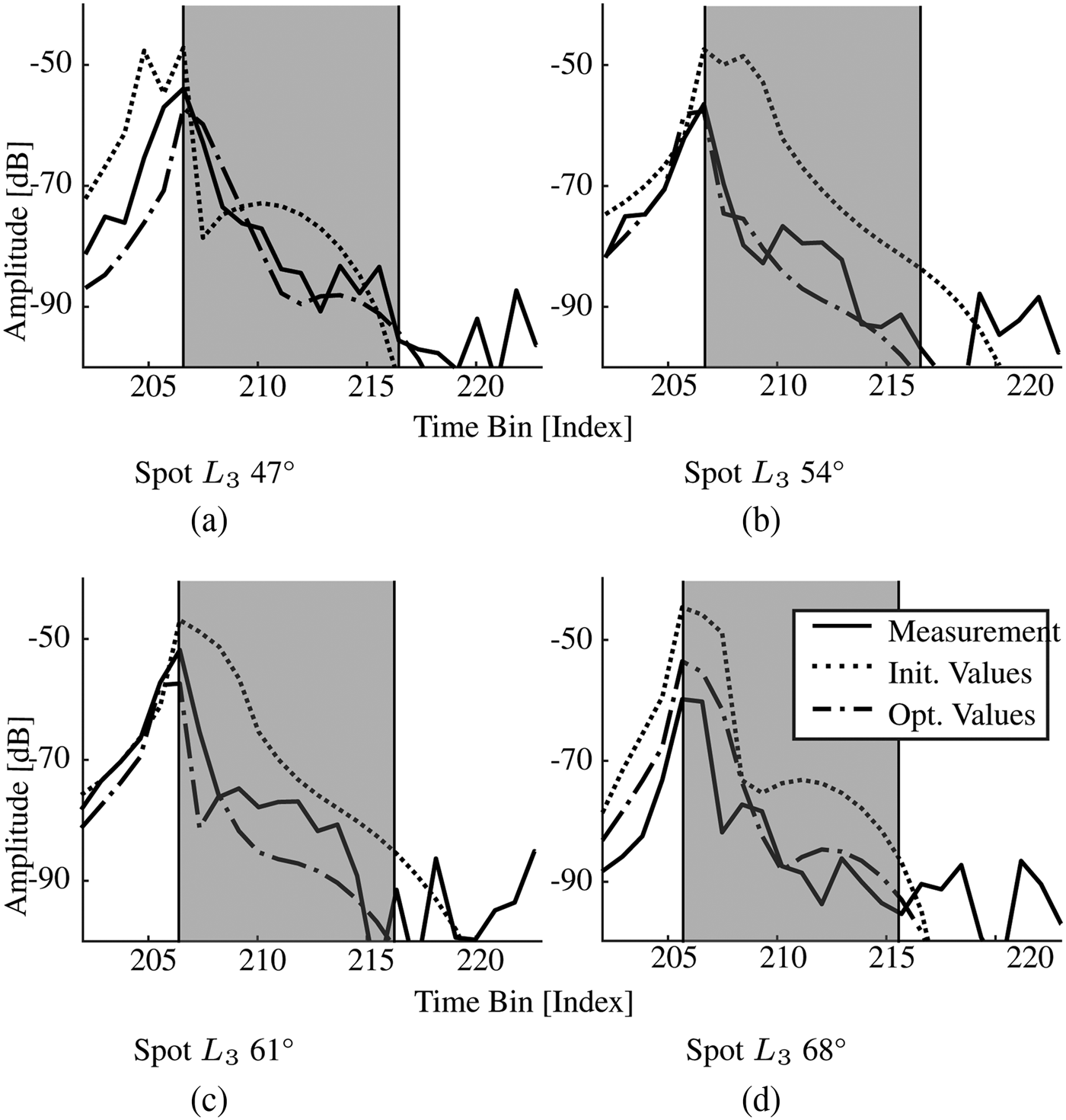
Table 4 shows the cost function of the scenarios when simulations with different parameter sets are compared with different measurements. The highlighted cells mark the cases where the parameter set is applied to its associated measurement scenario, i.e. the values are the same as summarized in Table 2. In the case of spots L 1, L 2, and L 3, the model performs best when calibrated with the parameters corresponding to the measurement it has been optimized with. In cases U 1 and U 2, the model reaches a comparable or even slightly better performance when parameter sets extracted for other spots are applied. For example, the parameter set derived for spot L 1 performs even better when compared with the measurements of spot U 1 with a decrease of the cost function from 74.3 to 60.8. However, the same does not hold for the reverse case: having a look at the performance of parameter set U 1 applied to the L 1 measurement leads to a significant drop in model performance, marked by an increase of the cost function from 51.2 to 100.1. These observations substantiate the observation that it is not possible to assign different parameter characteristics to different properties of the PCB surface.
Cross-comparison of model performance for varying measurements

Finally, Table 5 summarizes an evaluation of the obtained results by means of peak signal amplitude APeak and RMS delay spread τRMS which represent two widely applied quantities to describe the general form of a time-domain signal. The table provides the mean values of said quantities for all investigated AoIs of the reference group. The evaluation shows that despite the missing systematic behavior of the parameters, the general characteristics of the CIRs obtained from the model match those of the measurements extremely well. All of the compared amplitudes lie within ±2.5 dB deviation and the corresponding differences in RMS delay spread are clearly smaller than the temporal resolution of 20 ps at the considered bandwidth of 50 GHz.
Comparison of channel gain and RMS delay spread between the measured and simulated CIRs

Adoption to realistic propagation environments
In the calibration approach described above, the length of the reflected propagation path amounts to 120 cm with the point of reflection always being ata half distance. In general, both of these conditions are not met in realistic environments, e.g. with an antenna mounted close to a board surface communicating with another antenna on a different component inside a rather small piece of consumer electronics. Thus, upon implementation of the reflection model to a ray-tracing simulation platform, additional scaling needs to be applied to account for these effects. It should be mentioned that the modifications described in the following do not alter the model behavior for the calibration scenario.
In realistic environments, the amplitudes of the scatter components from (6) are modified according to
 $$a_{adjusted} = a \cdot \displaystyle{{1.2} \over D} \cdot sin^2\left( {\pi \cdot \displaystyle{{D_{Tx}} \over D}} \right){\rm }.$$
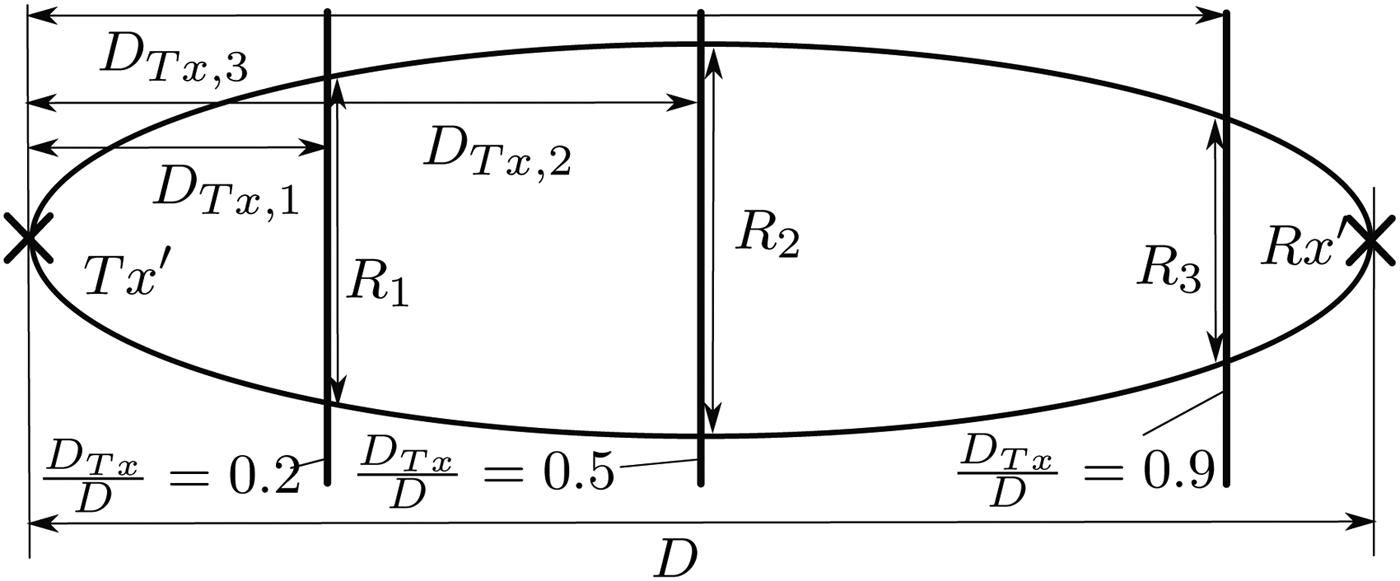
The first term of the normalization,  $\displaystyle{{1.2} \over D}$, accounts for the scaling of the total path length between Tx and Rx. As illustrated in Fig. 10, the diameter R of the ASR region linearly depends on the separation D between the antennas. Thus, this term accounts for the effect of a scaled ASR by inversely modifying the generated amplitudes. The sinusoidal term of (11) adjusts the size of the generated scattering area when the PCB surface is not at half distance between the antennas as illustrated in Fig. 11. The diameter of the intersection between the PCB and the ellipse around Tx and Rx reaches its maximum for a ratio of DTx/D = 0.5 while it approaches zero for the marginal cases when one antenna is located directly at the board surface. For illustrating the performance of the model in realistic environments, Figs 12 and 13 show the simulation results from an intra-device scenario in line-of-sight (LOS) and directed non-line-of-sight (dNLOS) configuration. The scenario comprises a cubic environment with a width of 26 cm, a height of 21 cm and a depth of 16 cm. The frame is made of Acrylonitrile Butadiene Styrene while two PCBs at a separation of 16 cm from its front and backside. A more detailed description along with the employed measurement approach can be found in [Reference Fricke, Achir, Le Bars and Kürner8]. The two dotted lines in each figure depict the measurement results of the respective scenario with a slight re-positioning of the antennas between the two measurement runs. The drawn-through line shows the result of the ray-tracing simulations. In case of the LOS scenario, the antennas have been placed directly opposing each other on the two PCBs. As seen in Fig. 12, the amplitude decay of the multiple signal bounces between the two boards is re-created very well, even though not all of the multipath components observed in the measurements are present in the simulated signals. The source of these echoes could be reflections from the employed measurement equipment or the ground plane of the laboratory which have not been regarded by the ray-tracing scenarios in the current configuration.
A larger antenna separation D 1 > D 2 leads to a larger diameter of the ASR R 1 > R 2.

The scattering radius Ri follows a squared-sine dependency on the ratio of DTxi/D.
Comparison of measurement and simulation in LOS configuration.

The same is the case for the results of the dNLOS geometry depicted in Fig. 13. In this configuration, both antennas have been positioned on the same PCB with their respective main lobe pointing at the specular reflection path via the board on the opposing side of the scenario. The main difference to the above case of direct transmission is that the peak signal is already the product of the guided first-order PCB reflection on the wall opposing the antennas. Again, the amplitude of the main signal as well as the amplitude decay of the multipath echoes is accurately captured by the ray-tracing simulations.
Comparison of measurement and simulation in dNLOS configuration.

Conclusion
In this study, a scattering model for the reflection of broadband THz signals from the surface of PCBs has been presented. Due to its straight-forward structure, the implementation of the model to any broadband ray-tracing algorithm is simple. The parameters of the model have been extracted based on measurements for different spots on the PCB using a simulated annealing process. Even though no direct relation between the four model parameters and the geometrical properties of the PCB could be established, the model is capable of producing results with a signal level and time-domain shape very close to that of actual measurements. Furthermore, examples for the successful implementation of the model to a ray-tracing algorithm have been provided.
Acknowledgement
The authors would like to thank Thomas Kleine-Ostmann of Physikalisch-Technische Bundesanstalt in Braunschweig for providing the 300GHz measurement equipment and expertise as well as Uwe Hellrung from the mechanical workshop of TUBS Institute for Communications Technology for constructing the mechanical setup required for the measurements.
 Alexander Fricke received his Diploma in Industrial Engineering (Major: Communications Engineering) from Technische Universität Braunschweig, Germany (TUBS) in 2011. Since 2012, he is working as a research assistant with the Institute for Communications Technology in the department for mobile radio systems at TUBS. His research interests lie in the field of THz communications, covering wireless channel modeling and system technology. Currently, he is dealing with channel modeling and PHY-layer design in the field of Terahertz intra-device communications. In this context, he had several contributions to the development of IEEE 802.15.3d TG 100G; moreover, he is the technical editor of the corresponding channel modeling document.
 Mounir Achir received an Engineer diploma, in 2001, from the Faculty of Electrical Engineering of the USTHB, Algiers, Algeria; The Master of Science degree in Telecommunication and Networking, in 2002, from the University of Pierre and Marie Curie (Paris VI), Paris, France; and the PhD degree in Telecommunication and Signal Processing, in 2005, from the National Polytechnic Institute of Grenoble, France. From 2005 to 2007, he was a Post-Doctoral Research Fellow in the wireless communication field first at Telecom Bretagne and after at the LIP6 (University of Paris VI). He joined the Canon Research Centre in France in 2007 where he is currently Chief Engineer and Team Leader. His research interests include wireless digital communications and Radar signal processing. He is the author and co-author of more than 15 papers and 40 patents.
 Philippe Le Bars received the engineering degree from Ecole Nationale Superieur dIngénieurs de Caen, Caen, France in 1982 and the Ph.D. degree in mathematics applied to signal processing and telecommunications from the University of Rennes 1, Rennes, France in 2012. In 1987 he Joined Apple Computer Research and Development in La Défense, France, where he was involved into the development of hardware of Public Switched Telephone Network modems for the portables and Performa computers. In 1997, he joined Canon Research Center France, Cesson Sévigné, France, as a Scientist, where he worked on error correction algorithms and hardware. He works now on antenna arrays and detectors at GHz and THz frequencies. He is the author and co-author of more than 35 US patents and 12 publications.
 Thomas Kürner received his Dipl.-Ing. degree in Electrical Engineering in 1990, and his Dr.-Ing. degree in 1993, both from University of Karlsruhe (Germany). From 1990 to 1994 he was with the Institut für Höchstfrequenztechnik und Elektronik (IHE) at the University of Karlsruhe. Since 2003 he is Full University Professor for Mobile Radio Systems with Institut für Nachrichtentechnik (IfN) at the Technische Universität Braunschweig. He participated in numerous European projects, amongst them is H2020-iBroW (Innovative ultra-BROadband ubiquitous Wireless communications through terahertz transceivers). Currently, he is chairing the IEEE 802.15 IG THz and has chaired the IEEE 802.15.3d TG 100G. Prof. Kürner is a member of the Board of Directors of the European Association on Antennas and Propagation (EurAAP). He is Associate Editor of IEEE Transactions on Vehicular Technology (since 2008) and IEEE Transactions on Antennas and Propagation (since 2017). In 2012 he was a guest lecturer at Dublin City University.



