

Introduction
High-power handling capabilities of GaN devices are advantageous for high-power amplifiers (HPA) [Reference Schuh1–Reference Duême3], but also for switches [Reference Campbell and Dumka4,Reference Bunz5] and robust LNAs [Reference Janssen6,Reference Schuh and Reber7]. All these devices are key components for T/R modules in AESA applications.
Figure 1 shows on the left hand a state-of-the-art T/R module frontend often still based on GaAs technology. Today's T/R modules still use a ferrite circulator to separate transmit and receive signals. To realize a high isolation between antenna and HPA on the one hand side and between low noise amplifier (LNA) and antenna on the other hand side, it is important that the LNA with limiter provides a good input match during TX mode and the HPA to provide a good output match during RX mode. The monolithic microwave integrated circuits (MMICs) are typically turned off during that mode of operation, respectively. For that reason a balanced HPA is often used, providing a good output match with the MMICs turned off. On the RX side, an additional PIN diode switch is used to guarantee a good input match during turn-off of the LNA. All these additional parts are not needed anymore when using a GaN-based MMIC switch, due to its higher isolation, when compared with the normally used available circulators. Using a switch results in a massive reduction of area on module level.
State-of-the-art hybrid GaAs-based frontend and new GaN-based single-chip frontend.
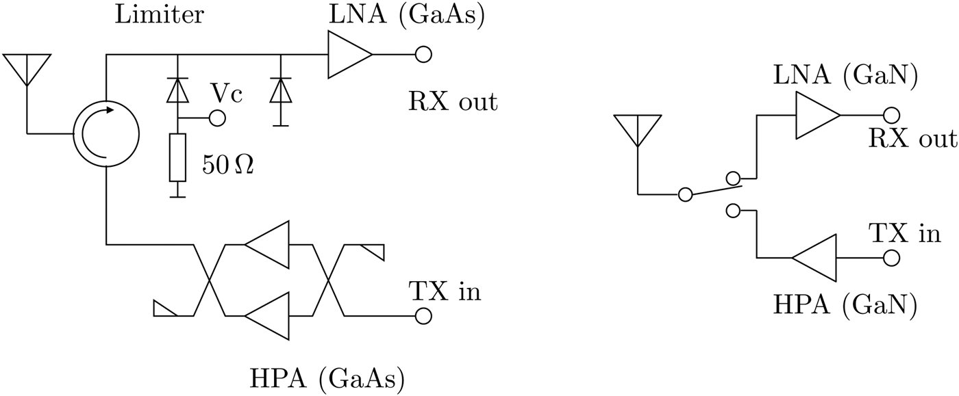
A new challenge for the HPA arises when using a switch. The HPA is not anymore isolated from the antenna. Signals coming from the antenna during TX mode are now reaching the output of the HPA. Therefore, this concept is suitable for robust GaN HPAs. GaAs-based HPAs very often are more sensitive to reverse power.
Because of the high-power handling capability of the used GaN technology, protection circuits in front of the LNA can be disclaimed. Today these protection circuits are often realized as hybrid assemblies using PIN diodes (see Fig. 1). Without this limiter an improvement of noise figure and a higher integration is feasible.
With this new frontend highly compact X-band T/R modules are feasible when combined for example with a highly integrated SiGe corechip [Reference Lohmiller8]. On the other hand also high performance T/R modules are possible, for example a polarization agile T/R module, because in the same geometrical size now a dual channel module is possible, where upto now only a single channel module fits.
The section “Frontend architecture” describes the architecture of the frontend chip, followed by a detailed description of each functional sub-block in the section “Design”. Measurement results for TX and RX mode are analyzed in the section “Measurement results” summarized by a conclusion in the section “Conclusions”.
Frontend architecture
On the right-hand side of Fig. 1 the block diagram of the GaN single chip frontend is shown. The frontend integrates the functions HPA, LNA, and SPDT switch. The SPDT switch connects the HPA output and LNA input to the antenna port. Switching is done with an user friendly interface. The target operating frequency range is at least 8 GHz to 12 GHz. The desired radio frequency (RF) output power at the antenna port is more than 13 W. To save PAE and RF output power, the SPDT switch is designed towards minimum insertion loss close to 0.8 dB in association with a maximum 0.1 dB compression point at 43 dBm RF power. The noise figure is designed close to 3 dB with a RX gain close to 14 dB.
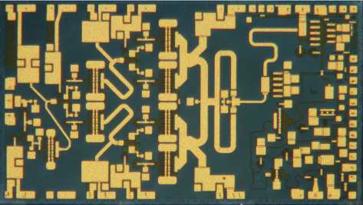
Figure 2 shows the realized GaN single-chip frontend. The transmitter part with a 3-stage HPA is located to the center-left of the chip. The TX input port is on the left edge. The bias ports of the HPA are positioned at the top and bottom edges of the chip, allowing a symmetrical biasing of the HPA. Top right is the SPDT switch and the antenna port. At the bottom right is the 2-stage LNA with RX output port. The interface for switch control is placed on the right side. With this arrangement, a very good isolation between TX and RX signal path is possible, especially taking into account the high TX gain. This high TX gain is necessary if the GaN frontend MMIC is directly combined with a SiGe corechip. Another advantage of this configuration is the very high on-chip integration density. The chip size is only 4.8 mm × 2.7 mm = 13 m m 2.
Chip photo of the single-chip GaN frontend.
Design
High power amplifier (HPA)
The major design goal for the X-band single-chip frontend was more than 13 Watt (41.2 dBm) over the whole frequency range from 8 GHz to 12 GHz. Considering the SPDT switch with 0.9 dB large signal insertion loss, more than 42 dBm HPA RF output power has been required. The maximum available output power of the applied GaN technology is close to 4W/mm. Therefore, the total gate width of the final HPA stage has been chosen to 4.8 mm (4 transistors each 8 × 150 μm).
A second important design goal was a TX incident power <20 dBm for the desired TX output power. Thus, the TX part of the GaN single-chip frontend requires a 3-stage amplifier.
The HPA design is a trade-off between maximum RF output power and power added efficiency (PAE), but with a clear emphasis to output power. Due to this, the second stage is three times smaller in gate width (2 transistors each 8 × 100 μm) than the final stage to save power consumption and to deliver still enough RF driver power over at least 40% bandwidth. The first stage includes a single 8 × 80 μm transistor, which is well matched to 50 Ω over the desired bandwidth.
The matching takes the stability conditions for amplifiers into account. Hence, typical resistive matching elements have to be applied to input and inter-stage matching networks. Furthermore, the resistive matching is optimized to ensure flat frequency response versus a large range of RF incident power.
Considering the compact amplifier design, coupling effects has been taken into account by electromagnetic (EM) simulations of all passive circuits.
Due to the missing isolation between antenna and HPA the loadpull behavior of the amplifier is gaining importance. In Fig. 3 the variation of the output power for different loads is shown. In addition, theoretical limits for an ideal amplifier with load independent available power are included. These limits are calculated according to equation (1), taking into account only the mismatch between amplifier and load. The measurement proofs that the HPA is not very load sensitive because the variation is only a little bit higher than the limits.
 $$L = \displaystyle{{\vert 1 - s_{22}\Gamma _{{\rm load}}\vert ^2} \over {1 - \vert \Gamma _{{\rm load}}\vert ^2}}$$
One advantage of a GaN HPA, compared with a GaAs HPA, is the improved robustness. It can withstand very high reverse power levels at its output. Normally, there is no need for an dedicated protection circuitry. For very harsh environments, an additional protection is possible by detecting the reverse power and changing the bias conditions [Reference van Heijningen9].
Measured TX output power variation for different load impedances.

Low noise amplifier (LNA)
The LNA is a two stage amplifier (see Fig. 4) with a noise match in the first stage by inductive source feedback. Using this technique noise match and input match over a wide bandwidth can be achieved and the loss of available gain is moderate. Both transistors have 240 µm gate width with a bias of 10 V and 25 mA, a good trade-off between power consumption and small signal gain. At lower drain voltage the small signal gain would be too low.
Principal schematic of the used LNA.

Excessive RF input power at the first transistor can cause damage due to increased gate current. This effect is evoked either by turn-on of the gate diode during forward conduction or by impact ionization break down under very high gate reverse voltage [Reference Rudolph10]. To count for maximum gate current rating in forward conduction the maximum available number of gates has been chosen for the input transistor because maximum gate current of the field effect transistor (FET) is proportional to the number of gates. Moreover, gate bias series resistors R 1 and R 2 were introduced to form a feedback which decreases gate current by shifting the gate voltage to more negative values. This also helps to keep the gate current within a safe limit.
With these measures the survivability of the GaN LNA is very high, but after a high-input overdrive pulse the LNA is changing its performance. The recovery time due to trapping effects can be very long [Reference Axelsson11]. With a special biasing electronic circuitry (patent-pending) it is possible to reduce the trapping itself and the recovery time to a sufferable level.
Despite the low drain current the maximum output power of a typical GaN LNA during input overdrive is normally higher than the maximum input rating of the following devices. In a typical T/R module application the affected components are either GaAs or SiGe-based and show damage levels in the range of 15 dBm to 20 dBm. These numbers are easily exceeded by the output power of conventional GaN LNAs [Reference Janssen6,Reference Schuh and Reber7]. Hence, some kind of protecting feature for susceptible components is required. A PIN diode limiter behind the LNA could do the job but cannot be implemented on the chip with our current technology. Introducing an extra PIN component is not attractive in the course of developing a low parts count module. Another approach which can be easily integrated is the introduction of a current source in the drain connections of the RF FETs. A small transistor running at I dss, which routes the drain current to the RF device (F3 and F4 in Fig. 4). The gate width and thus I dss of the small FET is chosen in a way that the drain current of the RF transistor is not limited under small signal condition. At large signal conditions the drain current tries to increase but is limited to a current slightly above the small signal value [Reference Schuh and Reber7].
Switch (SPDT)
The switch is the critical link between HPA and LNA and requires many trade-offs. Low loss and high isolation are contradicting. To achieve high overall TX efficiency the path to the HPA must be low loss and for LNA protection the isolation of the path to the LNA should be as high as possible. In RX mode, however, a minimal loss must be achieved for the LNA path to enable a low-noise figure. We decided to use an asymmetrical switch design with carefully selected gate width of the transistors (Fig. 5).
Principal schematic of the used asymmetrical switch.
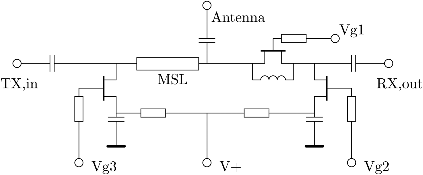
The TX path uses a transmission line with a switched short to open transformation. This configuration keeps the loss very low (typically 0.8 dB over the complete X-band) with sufficient isolation. Also a very high compression point is achieved. This is – together with a low insertion loss – important to obtain a high efficiency in TX mode.
In RX a bit more isolation is required to protect the LNA during TX pulse. Hence, a series-parallel-FET design has been selected. To keep insertion loss low a large series FET has been used, the resulting high off-capacitance must be resonated out. Otherwise the isolation would suffer.
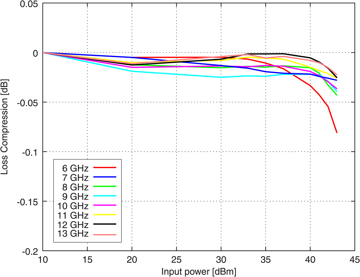
To prove these important features like loss or compression point of the switch a three port test structure of the switch core was also fabricated. The small signal measurement results in TX mode are shown in Fig. 6. A very low insertion loss (< 0.7 dB) is measured over the whole frequency range from 7 GHz to 12 GHz. The corresponding isolation between the TX and the RX path is better than 27 dB. The compression of the switch was measured using pulsed RF up to an input power of 43 dBm over a very large frequency band and a switch voltage of 28 V (see Fig. 7). A compression is hard to detect for frequencies above 6 GHz. For 43 dBm input power levels, compression values of 0.02 dB to 0.04 dB are achieved.
Measured insertion loss of the TX path and the isolation between TX and RX from the switch.

Measured compression behavior of the TX path from the switch.
A second focus of the design – other than good RF performance – is a user friendly interface which allows for a convenient control of the chip and a reduction of external components. Conventional GaN switch designs ask for a high negative control voltage to switch the FET devices [Reference Campbell and Dumka4]. A level shifter from positive digital signal to a complementary pair of negative signals is required. This design avoids negative control voltages through introduction of a positive offset voltage. This voltage is already available– it is the HPA drain supply. The source of parallel FETs are equipped with series capacitors which provide DC blocking and RF short.
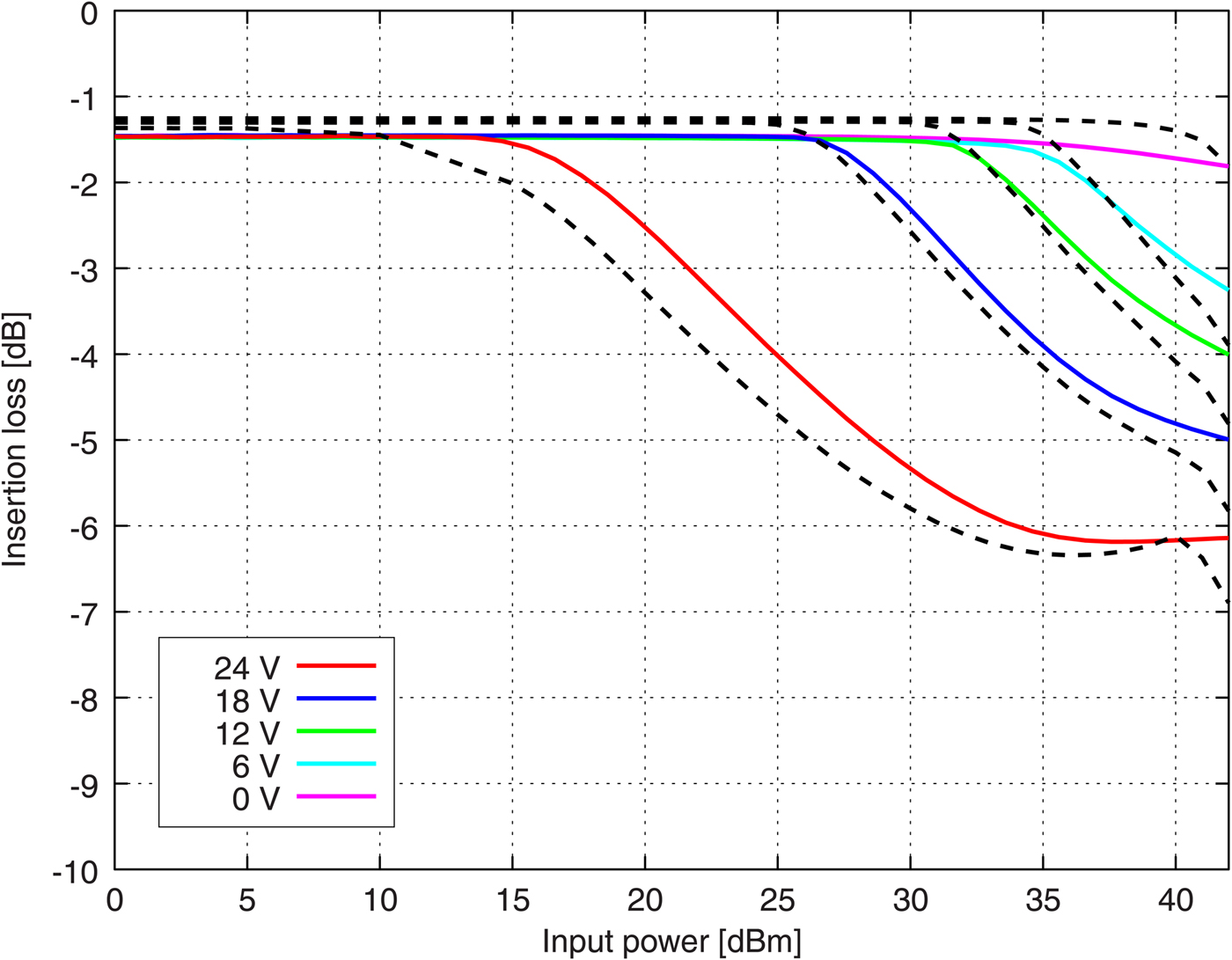
The offset voltage V+ is connected through isolation resistors similar to the connections of the control voltages of switching FET gates. During transmit F 1 and F 3 must be pinched off by pulling Vg 1 and Vg 3 to ground. This voltage is generated by an on-chip inverter. The input of the inverter is connected to the switched drain voltage of the HPA, and the output of the inverter to Vg 1 and Vg 3. The gate voltage of F 2 can be directly connected to the pulsed HPA drain. However, it is favorable for LNA protection not to use the full voltage swing at Vg 2. By pulling Vg 2 not completely to ground but only a few volts below V+, the series-FET F 2 has a lower compression level and will be turned on by high levels of input power during RX mode. In Fig. 8 the measurement and simulation results of this limiting function is shown for different Vg 2 voltages. A very good prediction by simulation is possible, the difference between measurement and simulation result is very small. With this circuit the insertion loss of the switch can be increased by 5 dB for large input power levels to further improve the robustness of the following LNA.
Measured compression behavior of the RX path from the switch in comparison with simulation results.
Measurement results
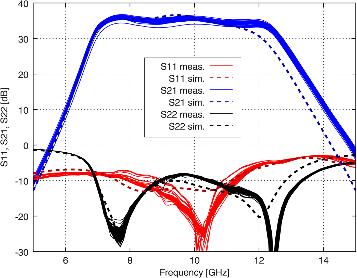
The measured TX linear gain is close to 35 dB with ± 1 dB ripple. This is in good agreement with respect to the simulation results (see Fig. 9). The basis for this good simulation prediction are accurate models for the transistors but also for the other passive circuit elements. For many passive circuit parts even EM simulations were used. Due to the availability of technology spread parameters Monte Carlo simulations are used to perform a design centering with respect to these spread values. At the upper frequency limit, the gain and also the output matching is even better than simulated. In Fig. 9, a whole wafer mapping is shown. The variation of the S-Parameters is very small. This indicates that the used semiconductor technology GH25 from UMS is very stable and well controlled during manufacturing.
Measured TX S-parameters in comparison with simulation results.
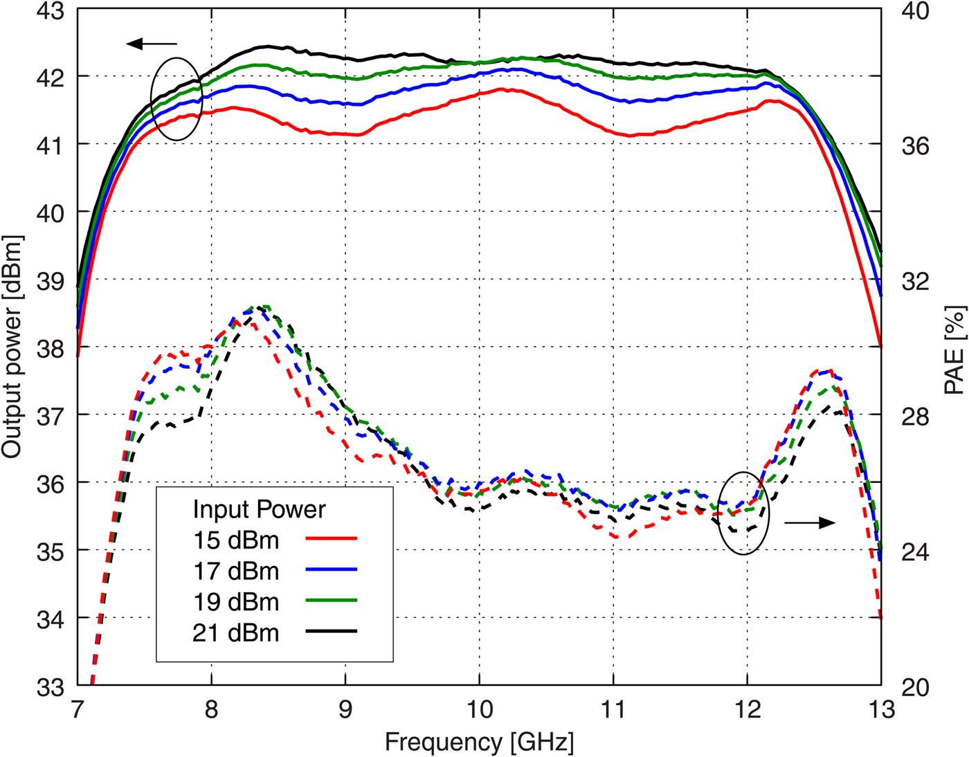
For an RF input power level of 15 dBm the measured RF output power at the antenna port exceeds 13 Watts within a bandwidth of 4.5 GHz and a small ripple of ± 0.25 dB (see Fig. 10). The associated PAE is more or less constant for a wide range of input power levels (up to 6 dB back-off). In Fig. 11 the simulated (dashed lines) and measured gain and noise figure of the frontend in RX mode is shown. The measurements show again the results of a whole wafer mapping and the variations for gain as well as noise figure are remarkably small. The obtained noise figure is very close to the expected one over a very large frequency band with a minimum value of 2.8 dB. Over the whole frequency range from 7 GHz to 12 GHz a noise figure below 3.2 dB is achieved. The measured gain of the LNA is well predicted by the simulation. Over almost the whole frequency range a gain higher than 14 dB is measured.
Measured TX output power and PAE for different input power levels.
Measured RX gain and noise figure in comparison with simulation results.
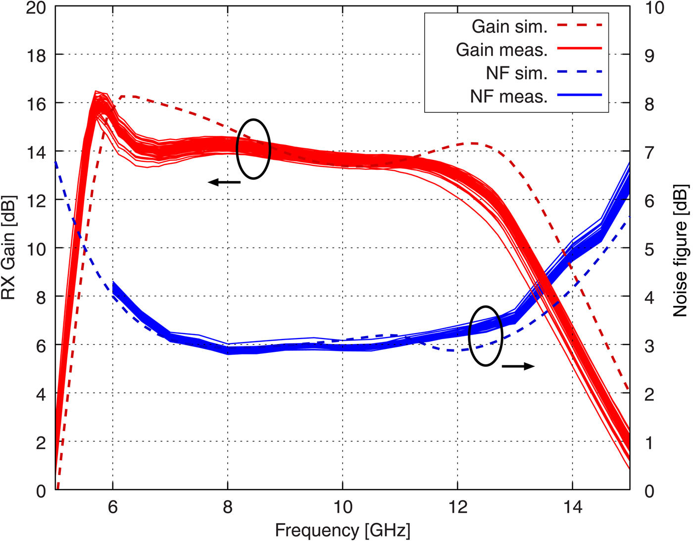
Figure 12 shows the effect of the limited current at the LNA drains. With the limiter activated a reduction of the maximum output power of 3 dB in minimum is possible, but the maximum RX output power of the frontend during massive input overdrive is still in the range of 23 dBm. Here the size of the limiting FETs still has to be optimized because a maximum output power below 20 dBm is desired. This current control has only a very little impact on the two tone linearity. The output third order intercept point (TOI) of the LNA is between 26 dBm and 28 dBm over the whole X-band (see Fig. 13).
Measured RX output power with and without current limiter.

Measured two tone output TOI with and without current limiter.

Conclusions
In this paper, we presented the design and measurement results of a single-chip frontend MMIC consisting of an HPA, LNA, and SPDT with an excellent performance.
A comparison of key performance parameters of the GaN single-chip frontend to other published state-of-the-art frontend MMICs is shown in Table 1. The achieved performance in noise figure and robustness is among the best results, even compared with single function GaN LNAs, especially when taking into account the low DC power consumption. In TX mode a very flat output power level higher than 13 W is achieved over a broad frequency range. The performance in TX and RX mode is very uniform over the frequency range from 7.7 GHz to 12.2 GHz.
Comparison of GaN-based X-band single-chip frontends

* Measured at f = 10.5 GHz only.
To our knowledge the performance of the single-chip frontend shown here is among the best results published up to now. The combination of this frontend with a SiGe corechip allows the realization of new compact high performance T/R modules.
Acknowledgments
This work was partly funded by the German Bundeswehr Technical Center for Information Technology and Electronics (WTD-81), Greding. The authors would like to thank all involved colleagues from HENSOLDT, Ulm for their strong support.
 Patrick Schuh received the Dipl.-Ing. degree and the Dr.-Ing. degree in electrical engineering from the University of Ulm, Germany, in 1998 and 2003, respectively, and the Masters degree in business administration from the University of Applied Sciences Neu-Ulm, Germany, in 2004.
From 1998 to 2002, he was a Research Assistant at the Institute of Microwave Techniques, University of Ulm, where his main research topic has been electromagnetic simulations for packages. Since 2002 he has been with the T/R-Modules & MMICs research department at EADS (now HENSOLDT) in Ulm, Germany. Since 2009 he is heading the GaN and SiGe group inside the department. In 2013 he is appointed as Expert for GaN based circuits & RF power modules. His current area of interest is MMIC and T/R-module design, especially high power amplifiers in GaN and GaAs technology.
 Hardy Sledzik received the Dipl.-Ing. degree and the Dr.-Ing. degree in electrical engineering from the University of Duisburg, Duisburg, Germany, in 1986 and 1990, respectively.
From 1986 to 1990, he was a Research Assistant at the Institute of Electromagnetic Theory and Engineering, University of Duisburg. Since 1990, he has been with EADS (now HENSOLDT) in Ulm, Germany. In 2016 he is appointed as Specialist for Integrated RF power amplifiers. His current area of interest is high power amplifier design, in GaN and GaAs technology.
 Rolf Reber received his Dipl-Ing. degree from the University of Karlsruhe, Germany.
He joined the Radar Group of AEG-Telefunken Ulm/Germany (which is now part of HENSOLDT) in 1987, where he has been engaged in the design and development of microwave components for active phased array antennas. In 2016 he is appointed as Specialist for T/R Module MMICs. His current work include the development and design of MMICs in SiGe-, GaAs- and GaN-technology dedicated for T/R-modules.


