


Introduction
Low-noise ultra-wideband amplifiers (low-noise distributed amplifier, LNDA) are not very common, but they are key components in several mm-wave and THz applications such as high-resolution radar, material spectroscopy, imaging systems, and fiber optic receivers. The frequencies of interest lie in the range of W-band (75–110 GHz), D-band (110–170 GHz), and G-band (140–220 GHz). As transistor speed has been increasing, with record performance exceeding 1 THz f max [Reference Lai, Mei, Deal, Yoshida, Kim, Liu, Lee, Uyeda, Radisic, Lange, Gaier, Samoska and Fung1–Reference Rode, Chiang, Choudhary, Jain, Thibeault, Mitchell, Rodwell, Urteaga, Loubychev, Snyder, Wu, Fastenau and Liu5], one can now realize integrated circuits in the terahertz frequency range (0.3–3 THz). Reports have been published on power amplifiers beyond 1 THz [Reference Mei, Yoshida, Lange, Lee, Zhou, Liu, Leong, Zamora, Padilla, Sarkozy, Lai and Deal6] for InP HEMT and 0.6 THz for InP HBT technology [Reference Hacker, Urteaga, Seo, Skalare and Lin7, Reference Seo, Urteaga, Hacker, Young, Skalare, Lin and Rodwell8]. The wide bandgap in the InP collector of an InP HBT provides a higher breakdown voltage as compared with HEMT devices. This feature makes it an attractive choice for high power sub-THz and terahertz amplifiers.
With respect to ultra-wideband LNDA, several publications can be found in the literature with bandwidths larger than the octave range: SiGe HBT [Reference Testa, Belfiore, Paulo, Carta and Ellinger9], GaAs mHEMT [Reference Pahl, Wagner, Massler, Diebold, Leuther, Kallfass and Zwick10], InP HBT [Reference Yoon, Lee, Urteaga, Kim and Jeon11], and CMOS [Reference Plouchart, Zamdmer, Sherony, Tan, Groves, Trzcinski, Talbi, Ray and Wagner12]. Several challenges exist in designing such ultra-wideband amplifiers, such as finding suitable topologies to achieve uniform forward gain response for the full band and a low-noise figure (NF) over this bandwidth, simultaneously. Another major challenge is to measure NF beyond 100 GHz and predict its behavior beyond this frequency.
In order to achieve wideband gain beyond the octave bandwidth, the distributed architecture is the most promising solution [Reference Ayasli, Vorhaus, Mozzi and Reynolds13]. Up to 235 GHz of bandwidth [Reference Eriksson, Darwazeh and Zirath14] have been reported. In this topology, the loss of an artificial microstrip transmission line is compensated by the gain cell, arranged periodically over the line. Using proper inter-stage line impedances, unit cell and termination resistance, uniform gain characteristics can be achieved. Although this type of amplifiers is not ideal for ultra-low-noise purposes, it solves the aforementioned challenges simultaneously. This work outlines the design and modeling of a distributed amplifier with the desired properties of both gain flatness and low-noise operation. A bandwidth of 40–185 GHz is achieved with an NF of 8 dB over a measured frequency range from 75 to 105 GHz. This paper is an extension of the paper published in [Reference Shivan, Hossain, Stoppel, Weimann, Schulz, Doerner, Krozer and Heinrich15]. The extensions comprise a large-signal model of the transistor, as well as a noise model. The former is applied in the optimization of the circuit for finding the best bias condition for the transistors. Furthermore, in distributed amplifiers there exist a trade-off between gain flatness and saturated output power which can only be assessed by a large-signal model. The latter is indispensable in explaining the noise measurements and predicting the NF outside the frequency range covered by the noise characterization set-up, particularly above its maximum frequency.
The organization of the paper is as follows: Section “InP DHBT process” presents the technology of the InP DHBT process and is followed by the transistor modeling in the section “Transistor modeling.” In the section “Noise modeling,” the NF predictive model is explained. In the section “Circuit design,” the circuit design is presented and the NF behavior versus frequency is predicted using the uncorrelated noise model. In the section “Measurements and discussion,” the measurement results are reported, covering small signal S-parameters, and NF. Finally, the section “Conclusions” presents the conclusions and the future work.
Technology
InP DHBT process
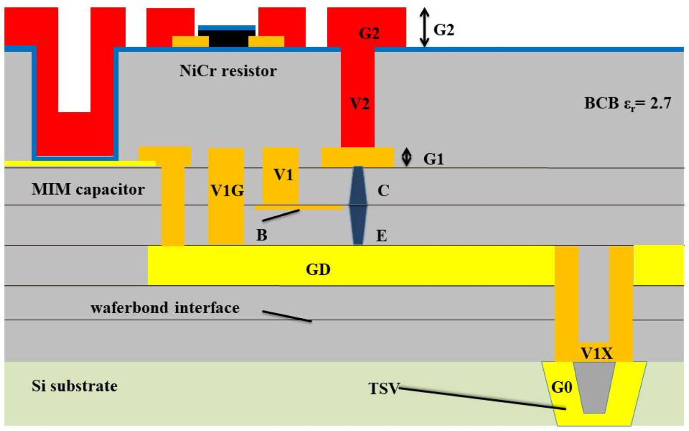
The circuit presented in this paper is based on the FBH transferred-substrate InP-DHBT technology, as illustrated in Fig. 1. The base-line process contains single and double finger InP/InGaAs DHBTs with 800 nm emitter widths [Reference Weimann, Stoppel, Schukfeh, Hossain, Al-Sawaf, Janke, Doerner, Sinha, Schmückle, Krüger, Krozer, Heinrich, Lisker, Krüger, Datsuk, Meliani and Tillack16]. Three layers of electroplated gold embedded in BCB are used as interconnects, ground plane, and microstrip lines, MIM capacitors with a capacitance of 0.3 fF/μm2 and NiCr thin film resistors with a sheet resistance on 25 Ω/sq. are used as passive elements. A high-resistivity silicon substrate with prefabricated through-silicon vias was used as host wafer in the wafer bonding process, which can be substituted with a fully processed BiCMOS wafer [Reference Weimann, Stoppel, Schukfeh, Hossain, Al-Sawaf, Janke, Doerner, Sinha, Schmückle, Krüger, Krozer, Heinrich, Lisker, Krüger, Datsuk, Meliani and Tillack16]. As a recent development down-scaled devices with 500 nm emitter widths and an optimized layout cell have become available. A single finger 0.5 × 6 µm2 InP/InGaAs DHBT biased at V CE = 1.5 V exhibits f t/f max values around 360/492 GHz, respectively, at a collector current density of 3.6 mA/μm2. The circuit presented in this paper is based on transistors with 500 nm emitter width.
Layer stack of transferred-substrate (TS) process.
Transistor modeling
The large-signal model topology proposed for the down-scaled transferred-substrate InP DHBT device is shown in Fig. 2. The FBH's custom HBT model forms the inner core of the large-signal model topology. Despite the fact that the FBH HBT model was originally developed for GaAs HBT devices (having a single base-emitter heterojunction) it has proven to be versatile enough to describe also DHBTs in the InP/InGaAs material system [Reference Johansen, Rudolph, Jensen, Kraemer, Weimann, Schnieder, Krozer and Heinrich17]. To extend the validity of the model structure toward higher millimeter-wave and THz frequencies, the model is embedded by an external network describing parasitic effects associated with via transitions and device electrodes within the layout cell itself [Reference Johansen, Doerner, Weimann, Hossain, Krozer and Heinrich18]. In this approach the elements of the external parasitic network are determined using full 3D electromagnetic (EM) simulation and include the skin-effect in the conductors and ultra-thin SiNx passivation layers in the stackup. The external parasitic network can be identified considering the EM simulation results from two structures only; (1) an open structure with the active layers of the InP DHBT removed and (2) a short structure in which the collector and emitter metallization are connected together. The EM simulation is performed to 325 GHz to accurately capture distributed high-frequency effects. The EM simulated results for the short structure is used to model the frequency dependent inductance and resistance of via transitions and device electrodes. The frequency dispersion in the extracted open structure capacitances versus frequency can be used to distribute the external network elements along the external device structure. The EM simulation assisted parameter extraction approach has the advantage over a purely measurement based approach that a significantly more complicated external network can be identified. This is because the EM simulation results are not corrupted by unwanted measurement artifacts such as probe-to-probe coupling, multimode propagation, and radiation associated with on-wafer characterization of small-size devices. Having identified the external parasitic network structure it can be used to embed the existing FBH HBT model structure for the InP DHBT devices. For convenience, the innermost reactive parasitic elements are absorbed into the FBH HBT model as shown in Fig. 2.
Large-signal model structure for 0.5 × 5.6 µm2 transferred-substrate InP DHBT.
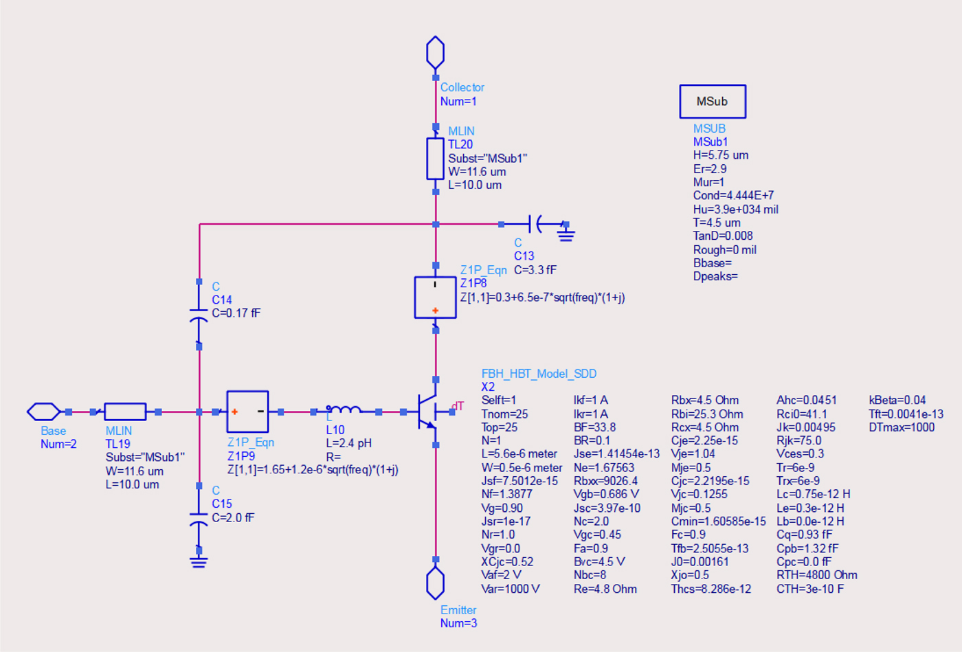
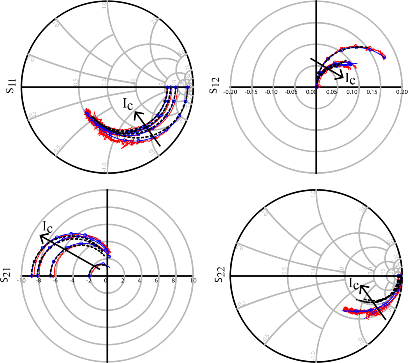
Following the extraction of the extrinsic parasitic network, the FBH HBT model parameters are determined based on measured multi-bias S-parameters and DC characteristics. The S-parameters used for extraction were corrected using on-wafer multi-line through-reflect-line (TRL) calibration setting the reference plane for model extraction at the boundary of the layout cell. Further de-embedding of the external parasitic network leads to an active device structure consistent with standard small-signal extraction techniques for HBTs [Reference Johansen, Doerner, Weimann, Hossain, Krozer and Heinrich18]. Figure 3 compares the multi-line TRL corrected S-parameters, measured from 50 MHz to 110 GHz, to the model response for bias points V ce = 1.5 V, I c = 0.9 mA, 5.4 mA, 9.6 mA, and 14.1 mA. In general, the proposed large-signal model structure is able to describe the measured data very well. The model response neglecting the external parasitic network is also shown in Fig. 3 using black dots. In general, the accuracy of the model suffers significantly above ~40 GHz. Of course, a traditional measurement based parameter extraction approach may absorb the external parasitic network elements into the FBH HBT large-signal model structure and the deviation between the modeled response and the measurements may not be as significant as shown in Fig. 3 (see [Reference Johansen, Rudolph, Jensen, Kraemer, Weimann, Schnieder, Krozer and Heinrich17] for an example using 0.8 × 5.6 µm2 InP DHBTs). It is however important to stress that such a modeling approach is fundamentally incorrect and the lack of distribution of the parasitic elements along via transitions and device electrodes will limit the validity of the model at higher frequencies.
Measured (red solid lines) and modeled (blue solid lines with circles) S-parameters from 50 MHz to 110 GHz at the bias points: V ce = 1.5 V at I c = 0.9, 5.4, 9.6, and 14.1 mA.
Noise modeling
Predicting the noise performance of a circuit requires noise models describing the noise sources present in the circuit. Besides all resistances exhibiting thermal noise, a proper description of the shot noise at the HBTs pn junctions is required. Since the shot-noise power is directly linked to the DC current and the chip temperature controls the thermal noise, noise modeling remains tedious only for the following two reasons: the high frequencies require highly accurate modeling of distributed effects, and the correlation between the shot-noise sources needs to be known very well. The first issue is not specific to noise, and it is taken care of as discussed in the previous sections on HBT modeling and circuit design. The second issue is related to the question of how close the noise of the base-collector junction is correlated with the noise originating in the base-emitter junction.
Shot noise sources are commonly implemented as shown in Fig. 4 [Reference Fukui19]. The model assumes that the shot noise at both junctions originates basically from the same current and can therefore be considered to be correlated [Reference Fukui19, Reference Ziel20]. The correlation is linked to the base-collector transport time and can be described by an equivalent noise correlation time delay τ n. This time constant can vary between a fraction of the base-collector transit time τ bc down to ωτ n ≈ 0, which is a common assumption implemented in traditional large-signal noise models since it is very easy to code [Reference Fukui19].
Equivalent circuit of the intrinsic HBT including shot-noise sources and thermal noise source of the intrinsic base resistance.

The only degree of freedom in the noise modeling therefore is the noise correlation time constant τ n, which requires to be determined from measurement. For III-V HBTs, we found τ n to almost equal time-delay τ bc of a InGaP/GaAs HBT operating at L-band [Reference Rudolph, Doerner, Klapproth and Heymann21], but to decrease to a small fraction of τ bc with shrinking layer thickness and increasing cut-off frequencies for these devices [Reference Rudolph, Korndörfer, Heymann and Heinrich22]. For the transferred-substrate DHBT technology used in this work, noise parameters were measured up to 26 GHz in order to investigate the noise properties, especially regarding τ n. It was found that τ n close to the base-collector transit time yields lower minimum NFs toward higher frequencies compared with the approximation ωτ n ≈ 0 which is predicting a steeper slope [Reference Kaule, Doerner, Weimann and Rudolph23].
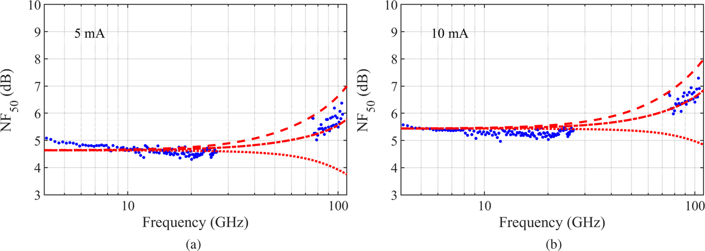
In the course of this work, 50-Ω NF (NF50) was measured in the frequency range of 75–105 GHz in order to validate the model's extrapolation capability. Figure 5 shows the measurement together with NF50s calculated from the measured noise parameters up to 26 GHz reported in [Reference Kaule, Doerner, Weimann and Rudolph23] (bullets) compared with simulated values (lines). The device under test was a single-finger transfer-substrate InP DHBTs with an emitter area of 0.8 × 6 µm2 measured at the same bias points as used in the design of the circuit. The simulations reveal the impact of the noise correlation time constant on the actual NF around 100 GHz. As expected from our previous work, the predicted slope of NF50 increases with decreasing τ n. Apparently, higher τ n allow the noise contribution of the two pn-junctions to cancel out as frequency increases. The figure shows three possible model assumptions: the dashed line corresponds to τ n = τ bc, and the dashed line corresponds to ωτ n ≈ 0. The dash-dotted line in between was simulated assuming τ n = 0.25 τ bc. The measurement beyond 26 GHz, however, was performed together with the measurement of the amplifier, as discussed below. For the design, the noise model was used to extrapolate the noise behavior beyond 26 GHz assuming ωτ n ≈ 0. It was not only in line with the 26 GHz-measurement, but also easily coded into the model since it did not require any estimate of transit times. And even though this assumption is underestimating τ n which would be in the range of 0 < τ n < 0.25τ bc by lightly more than 0.5 dB at 50 Ω, we consider the model very well suited in practical circuit design where it might be advantageous to be on the safe side.
Measured (bullets) and simulated NF50 of a single-finger InP DHBT at (a) I c = 5 mA and (b) I c = 10 mA at V ce = 1.5 V. Dotted line: simulation assuming that τ n equals of the base-collector time delay, dash-dotted line: a quarter of total time delay, and dashed line assuming ωτ n ≈ 0.
Circuit design
To achieve ultra-wideband gain characteristics and low noise throughout the bandwidth, a distributed architecture with five unit cells is chosen, as shown in Fig. 6. The unit cells comprise two single-finger 0.5 × 6 µm2 transistors arranged in a cascode configuration [Reference Shivan, Hossain, Stoppel, Weimann, Schulz, Doerner, Krozer and Heinrich15].
Simplified circuit schematic (V b1, V b2, and V c are the DC bias for the circuit).

The cascode configuration improves the gain-bandwidth product (GBP) by reducing the Miller effect. As a result, the input capacitance is lowered and input-to-output isolation is boosted. Several approaches have been taken to improve the GBP, among which introducing a small inductance in the form of a transmission line, L e, helps to increase the gain at higher frequencies. The optimum value of L e = 20 µm for each unit cell was determined by studying gain and stability factor as a function of frequency, as shown in Fig. 7. The artificial transmission lines L a and L b are chosen such that the maximum gain-bandwidth is achieved. Since the transistor is matched differently at input and output, the line segments, L a and L b, have widths of 22 and 7 µm, respectively.
Simulated S 21 and stability factor of a cell versus frequency, varying line length L e from 0 to 50 µm [Reference Shivan, Hossain, Stoppel, Weimann, Schulz, Doerner, Krozer and Heinrich15].
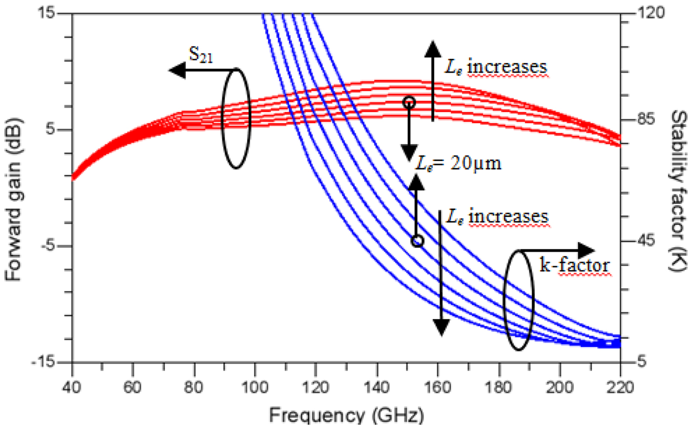
To obtain high gain, the transistor, T ce, is arranged in the common-emitter configuration without source degeneration. This improves the overall gain of the transistor in exchange of gain flatness. Since the f t/fmax values of the 500 nm transistor are ~360/492 GHz, respectively, the circuit gain performance deteriorates around 185 GHz. In order to obtain flat gain characteristic with stable operation, a small inductance in the form of a transmission line, L cb of length of 120 µm, is introduced between the transistor, T cb, and the upper transmission line, L a. This optimum value has been found by simulating the forward gain and k-factor of each cell and varying L cb, as illustrated in Fig. 8.
Simulated forward gain (S 21) and stability factor of each cell versus frequency, varying line length L cb from 40 to 200 µm [Reference Shivan, Hossain, Stoppel, Weimann, Schulz, Doerner, Krozer and Heinrich15].

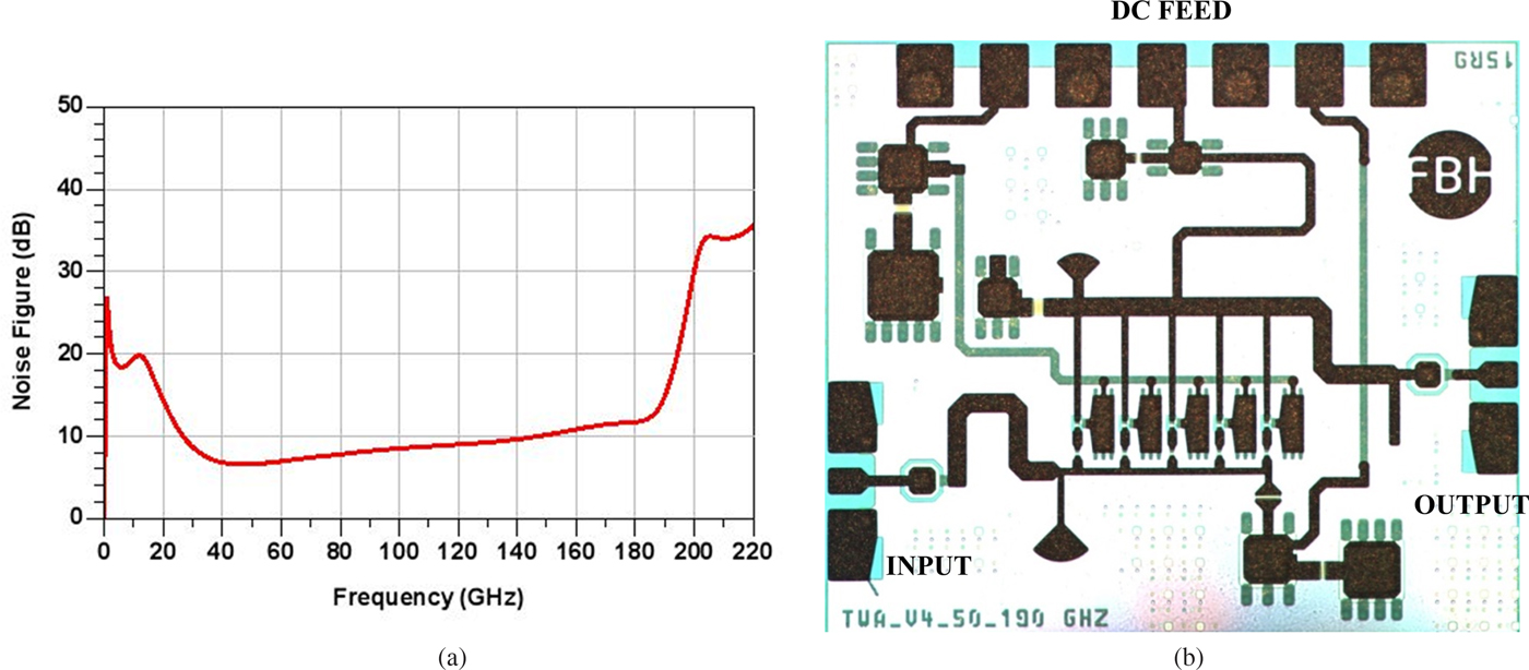
In a cascode configuration, the capacitor C b of the common-base transistor T cb can be tuned for optimum gain and output power. When increasing the value of C b, the gain flatness at higher frequencies is improved, at the expense of saturated output power. From simulations, an optimum value of 400 fF is chosen as the best compromise between bandwidth and output power. The termination resistances, R term1 and R term2, are chosen as 30 and 20 Ω, respectively, providing the best input and output reflection match. Finally, matching stubs, L stub1 and L stub2 of lengths 50 and 75 µm, respectively, were used to further improve input and output matching. An input matched line L m of length 200 µm additionally enhances input matching for the frequency band from 40 to 185 GHz. After all the adjustments for gain-flatness and GBP improvement, the resulting NF is plotted against frequency, as presented in Fig. 9(a). The simulated NF indicates a fairly uniform behavior over the frequency range with a value less than 10 dB up to 150 GHz. A photograph of the circuit is provided in Fig. 9(b).
(a) Simulated NF of circuit versus frequency. (b) Photograph of the distributed amplifier (0.8 × 0.75 mm2) [Reference Shivan, Hossain, Stoppel, Weimann, Schulz, Doerner, Krozer and Heinrich15].
Measurements and discussion
Small signal measurements
Small-signal measurements were performed using off wafer calibration for DC-140 GHz and on-wafer calibration for 140–220 GHz using 50 µm pitch GSG probes in both cases. The measured S-parameters are plotted against the simulation data in Fig. 10. Using the model parameters as obtained from the section “Transistor modeling,” there is very close agreement between simulation and measurement. The small difference at the highest frequency range is due to process variation which leads to higher attenuation of the transmission lines beyond 150 GHz.
(a) Simulated (solid line) and measured (dotted line) S-parameters and (b) measured stability factor [Reference Shivan, Hossain, Stoppel, Weimann, Schulz, Doerner, Krozer and Heinrich15].
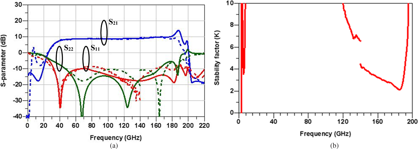
The forward gain, S 21, is relatively flat with an average value of 10 dB with a variation of only ±1.5 dB from 40 to 185 GHz. This flatness is the result of the appropriate choice of gain peaking inductances as discussed in the previous section. In the simulation of S 21, a peaking is observed at 185 GHz which comes from a too low line loss prediction at high frequencies. This is absent in the measurements where the real line losses are high enough to suppress this effect.
The cut-off frequency of the input transmission line with input capacitance plays an important role regarding the upper limit of the BW (up to 185 GHz). The cut-off frequency of the input lines in around 200 GHz which is lower than 0.5 × f max of the transistors. Therefore, the circuit is currently limited in BW by the input transmission line. The reflection parameters, S 11 and S 22, are both around −10 dB in the range 60–170 GHz. For the remaining operating range of 40–60 GHz and 170–185 GHz, the matching is below −5 dB. There is a peaking at low frequencies around 7 GHz, as can be seen from Fig. 10. This is due to insufficient decoupling from the DC-sources during measurements. The k-factor exceeds 3.5 at these frequencies, as can be seen in Fig. 10(b), which proves that the peaking is not caused by oscillations from the circuit. The circuit has a minimum k-factor of 2.2 at 190 GHz, indicating stable operation throughout the entire frequency range. The total DC power consumption was approximately 96 mW.
Noise figure measurement setup
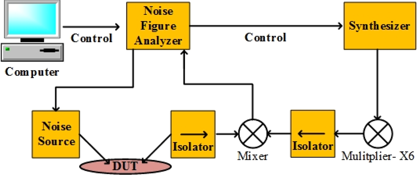
The on-wafer noise measurements were performed at Fraunhofer Institute IAF in Freiburg, Germany. The setup shown in Fig. 11 comprises a commercial mixer module, whose local oscillator input is driven by a multiplied synthesizer signal. The NF analyzer controls the synthesizer as well as the noise source and evaluates the down-converted signals. A similar measurement setup for NF measurements in the D-band has been reported in [Reference Weber, Massler and Leuther24].
NF measurement setup.
Measured data and comparison with simulations
An essential feature for the successful design of an ultra-wideband LNDA is the underlying noise model for the transistors. These models are usually based on the measurement of the four noise parameters using a source-pull setup, which usually is limited to rather low frequencies up to 26 or 105 GHz at best. The design of this ultra-wideband LNDA was therefore based on an extrapolation of a model carefully determined up to only 26 GHz. The good prediction of the LNDAs noise performance prove the validity of the model assumptions up to 100 GHz and beyond, which provides an important contribution to the noise modeling of InP HBTs.
The NF measurements for the frequency range from 75 to 105 GHz are plotted in Fig. 12. The NF is fairly constant with an average value of 8 dB and a variation of ±0.3 dB within this frequency range. This result indicates the circuit's potential for low-noise performance over a very high bandwidth. Even though InP DHBT-based circuits exhibit inferior noise performance as compared with HEMT devices, the results presented here highlight the potential of InP DHBT for ultra-wideband low-noise applications above 100 GHz.
Measured (solid line) and simulated NF50 of the LNA. Dashed line: simulation with noise model assuming τ n = 0, dotted line: simulation assuming τ n = τ bc.

As discussed above, noise performance was optimized using a noise model neglecting the noise correlation time constant τ n, depicted by the dashed line in Fig. 12. This curve shows excellent agreement within the estimated range of measurement uncertainty. As a comparison, a post-fabrication simulation was performed assuming τ n = τ bc, see dotted line in Fig. 12. This predicted NF is lower, as expected from the investigation of the noise model. The difference in NF obtained with the two model assumptions, however, is less than suggested from the difference in predicted NF50 of the device, which is about 3 dB at 105 GHz as seen in Fig. 5. This is caused by the fact that the assumption made for τ n affects all four noise parameters including optimum noise match.
With reference to Fig. 10, the measured and simulated gain, S 21, and input match, S 11, agree very well. The graph also proves the good quality of the model in terms of predicting the LNDA behavior, but also verifies that the input matching assumed in circuit design was actually realized in the fabrication of the chip. Overall, the LNDA results prove that the modeling assumption based on noise-parameter measurement up to 26 GHz are valid and provide excellent prediction of the noise behavior up to 105 GHz. It is safe to conclude that the proposed noise model will remain valid up to the maximum frequency for which the underlying small- or large-signal model predicts the behavior with good accuracy. As stated before, even though the HBTs minimum NF is increasing with frequency due to the low-noise correlation time constant τ n, the results obtained with this circuit prove that they are competitive devices for LNDA design.
Table 1 benchmarks the state-of-the-art ultra-wideband LNDAs, arranged in the order of decreasing bandwidth. We note that our circuit has outstanding attributes when compared with the state-of-the-art regarding several metrics: first, it has very high 3-dB bandwidth reported for a single-stage cascode based DA. Second, this circuit exhibits one of the lowest W-band NF values among ultra-wideband LNDA, while going up in frequency to the D-band. Moreover, it has very low DC power consumption in this class of circuits. In terms of NF, the circuit achieves a value of 8 dB which is fairly constant in the 75–105 GHz range. From the literature, it is seen that the NF increases with increasing frequency beyond 60 GHz [Reference Testa, Belfiore, Paulo, Carta and Ellinger9, Reference Eriksson, Darwazeh and Zirath14, Reference Zech, Diebold, Wagner, Schlechtweg, Leuther, Ambacher and Kallfass25–Reference Fritsche, Tretter, Carta and Ellinger27]. Therefore, an NF value of 8 dB is close to the lowest reported NF in W-band for such ultra-wideband LNDAs. Among the circuits in Table 1, only [Reference Hoffman, Voinigescu, Chevalier, Cathelin and Schvan26] presents a lower NF in W-band than our work, however, it covers DC-135 GHz and thus a lower frequency range than our work, which includes the full D-band. Regarding bandwidth, [Reference Testa, Belfiore, Paulo, Carta and Ellinger9, Reference Eriksson, Darwazeh and Zirath14, Reference Fritsche, Tretter, Carta and Ellinger27, Reference Li, Goh, Tang, Liu, Deng and Xiong28] yield higher bandwidth but the NF values are either worse or not provided in the W-band. In terms of RF power, the maximum RF output power, P sat, of 10 dBm at 160 GHz makes the circuit a potential candidate for ultra-broadband, low-noise high-power applications covering W-band and D-band simultaneously. Reports of high and uniform output power of DA using the same technology has been published for lower frequency range [Reference Shivan, Weimann, Hossain, Stoppel, Boppel, Ostinelli, Doerner, Bolognesi, Krozer and Heinrich29].
State-of-the-art of ultra-broadband LNDA with reports of low noise (gain > 7 dB).

a Multi stage distributed amplifier.
Conclusions
In this paper, the design of an ultra-broadband LNDA with a low noise is analyzed, which exhibits a high output power P sat of 10 dBm at 160 GHz as well as good low-noise performance, a circuit NF of 8 dB in the 75–105 GHz range and a very low DC power consumption. This work has two-fold novel information regarding the design of ultra-broadband LNDAs. One aspect is the design of the circuit itself which covers both W-band and D-band with high-power characteristics and low-NFs in the W-band. The other aspect is the verification of the noise model which can reliably predict the NF beyond the scope of measurement facility.
Author ORCIDs
T. Shivan, 0000-0003-2555-5400.
Acknowledgement
This research was supported by the Helmholtz Research School on Security Technologies (HRSST) and by Leibniz association under SAW project “InP THz HBT.” The authors would like to thank the team at Fraunhofer IAF, especially Hermann Massler, for their support regarding the noise measurements. The authors would also like to acknowledge the partial financial support by the H2020 EU project ULTRAWAVE contract no. 762119.
 Tanjil Shivan was born in Dhaka, Bangladesh, in 1986. He received his Master's degree in electrical engineering from the Chalmers University of Technology, Sweden, in 2013. From December 2013 to April 2014, he was working as a research assistant in the department of Signals and Systems, Chalmers University of Technology, Sweden. There he developed novel GAP-waveguides for 220–325 GHz frequency range. From May 2014 he has been working as a Doctoral Candidate at Ferdinand Braun Institute, in Berlin, Germany. His research is focused on ultra-broadband component design in the frequency range of DC-325 GHz.
 Evelyne Kaule received her B.Sc. and M.Sc. degrees in electrical engineering from the Brandenburg University of Technology Cottbus – Senftenberg, Cottbus, Germany, in 2014 and in 2017. Since then, she has been with the Brandenburg University of Technology Cottbus – Senftenberg, Cottbus, Germany, where she is currently a Doctoral Researcher.
 Maruf Hossain received his M.Sc. degree in Electronics/Telecommunication from the University of Gavle, Gavle, Sweden in 2008 and his Ph.D. degree in Electrical Engineering from the Technical University of Berlin (TUB), Berlin, Germany in 2016. In 2008, he joined IHP microelectronics in the circuit design department, Frankfurt/Oder, Germany. Since 2011, he has been with Ferdinand-Braun-Institut (FBH), Berlin, Germany. His research interests include CMOS/BiCMOS, millimeter wave, and THz circuit design and characterization.
 Ralf Doerner received his Dipl.-Ing. degree in communications engineering from the Technische Universität Ilmenau, Ilmenau, Germany, in 1990. Since 1989, he has been working on microwave measuring techniques. In 1992, he joined Ferdinand-Braun-Institut, Leibniz-Institut für Höchstfrequenztechnik, Berlin, Germany. His current research is focused on calibration problems in on-wafer millimeter-wave and sub-millimeter-wave measurements of active and passive devices and circuits. Further research activities include nonlinear characterization of microwave power transistors and noise characterization and modeling of microwave devices. He received the 71st ARFTG Best Interactive Forum Paper Award and the 2011 European Microwave Prize.
 Tom K. Johansen received his M.S. and Ph.D. degrees in electrical engineering from the Technical University of Denmark, Denmark, in 1999 and 2003, respectively. In 1999 he joined the Electromagnetic Systems group, DTU Elektro, Technical University of Denmark, Denmark, where he is currently an Associate Professor. From September 2001 to March 2002 he was a Visiting scholar at the center for wireless communication, University of San Diego, California, California. He has spent several external research stays at the Ferdinand Braun Institute (FBH), in Berlin, Germany. His research areas include the modeling of high-frequency solid-state devices, millimeter-wave, and sub-millimeter-wave integrated circuit design.
 Dimitri Stoppel received his B.Eng. in Microsystems Technology and his M.Eng. in Systems Engineering from the University of Applied Sciences, Berlin, Germany, in 2012 and 2013, respectively. From 2013 to 2018 he was working on process development for InP-DHBT MMIC processes as a Ph.D. student at Ferdinand-Braun-Institut, Berlin. Currently he is working as a Product Quality Engineer for small signal MOSFETs at Nexperia GmbH, Hamburg, Germany.
 Sebastian Boppel received his Diploma degree in Physics from the University of Heidelberg, Germany, in 2008, and his Ph.D. degree from the Goethe-University, Frankfurt am Main, Germany, in 2013. He was awarded the Gernot-und-Carin-Frank-Prize for the best dissertation of the year. From 2008 to 2016, he was member of the Ultrafast Spectroscopy and Terahertz Physics group of Goethe-University, Frankfurt am Main, Germany. During this time, he authored and co-authored more than 50 papers, conference contributions and talks, two patents and one book chapter on field-effect-transistor-based THz detection. In 2016, he started working on InP-based terahertz electronics and is currently heading the InP Devices Lab at the Ferdinand-Braun-Institut, Leibniz-Institut für Höchstfrequenztechnik, Berlin, Germany.
 Wolfgang Heinrich received his diploma, Ph.D., and habilitation degrees from the Technical University of Darmstadt, Germany. Since 1993, he has been with Ferdinand-Braun-Institut (FBH) at Berlin, Germany, where he is head of the microwave department and deputy director of the institute. Since 2008, he is also professor at the Technical University of Berlin. His present research activities focus on MMIC design with emphasis on GaN power amplifiers, mm-wave integrated circuits, and electromagnetic simulation.
Prof. Heinrich has authored or coauthored more than 350 publications and conference contributions. He has been serving the microwave community in various functions. From 2010 to 2018, he has been President of the European Microwave Association (EuMA).
 Viktor Krozer (M'91–SM'03) received his Dipl.-Ing. and Dr.-Ing. degree in electrical engineering at the Technical University Darmstadt in 1984 and in 1991, respectively. In 1991 he became senior scientist at the TU Darmstadt working on high-temperature microwave devices and circuits and submillimeter-wave electronics. From 1996 to 2002 Dr. Krozer was a professor at the Technical University of Chemnitz, Germany. During 2002–2009 Dr. Krozer was professor at Electromagnetic Systems, DTU Elektro, Technical University of Denmark, and was heading the Microwave Technology Group. During 2009–2012 Dr. Krozer has been an endowed Oerlikon-Leibniz-Goethe professor for Terahertz Photonics at the Johann Wolfgang Goethe University Frankfurt, Germany and since 2012 heads the Goethe-Leibniz-Terahertz-Center at the same university. He is also with FBH Berlin, leading the THz components and systems group. His research areas include terahertz electronics and imaging, MMIC, nonlinear circuit analysis and design, device modeling, biomedical sensors, and remote sensing instrumentation.
 Matthias Rudolph received his Dipl.-Ing. degree in electrical engineering from the Berlin Institute of Technology, Berlin, Germany, in 1996, and his Dr.-Ing. degree from the Darmstadt University of Technology, Darmstadt, Germany, in 2001. In 1996 he joined Ferdinand-Braun-Institut, Leibniz Insitut für Höchstfrequenztechnik (FBH), Berlin. In October 2009, he was appointed the Ulrich-L.-Rohde Professor for RF and Microwave Techniques at the Brandenburg University of Technology, Cottbus, Germany. His research focuses on modeling of FETs and HBTs and on design of power, broadband, and low-noise amplifiers.


 Open access