












Introduction
Digital transmitters (DTXs) are attractive for sub- ${6}\,\mathrm{GHz}$ wireless systems because RF signal generation can be implemented largely with digital logic and switch-mode power amplifiers (PAs) in nanoscale CMOS [Reference Sheth, Zhang, Shen, Iyer and Bowers1, Reference Li, Li, Yin, Yan, Qi, Liu and Xu2]. This approach supports high integration, operation at low supply voltages, and digital reconfiguration for multiband and multimode use [Reference Beikmirza, Shen, de Vreede and Alavi3, Reference Beikmirza, Shen, de Vreede and Alavi4]. Modern standards, however, employ wideband orthogonal frequency-division multiplexing (OFDM) and high-order quadrature amplitude modulation (QAM) with large peak-to-average power ratio (PAPR). These waveforms tighten constraints on back-off efficiency and spectral linearity, typically reported as adjacent-channel leakage ratio (ACLR) and error vector magnitude (EVM).
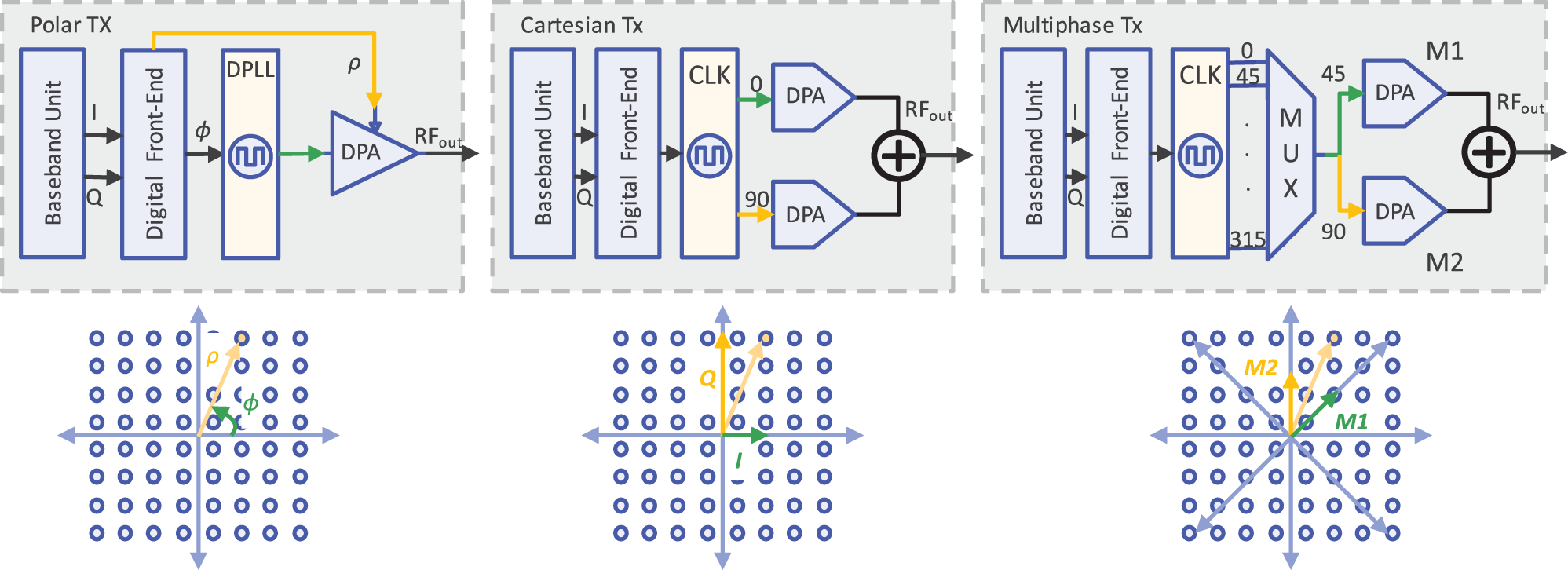
Figure 1 compares three representative DTX architectures and their trade-offs. Polar DTXs separate amplitude and phase modulation and can improve efficiency, but wideband operation is limited by Cartesian-to-polar nonlinearity, bandwidth expansion, and stringent AM–PM alignment [Reference Li, Li, Yin, Yan, Qi, Liu and Xu2, Reference Hu, Yin, Li, Liu, Xiong and Xu5, Reference Zhang, Liu, Li, Tang, Zhang, Huáng, Xu, Madany, Fadila, Wang, Xiong, Zhang, Kusuma, Sakai, Kunihiro, Shirane and Okada6]. Quadrature (Cartesian) DTXs avoid the coordinate transformation and support wideband complex modulation, but orthogonal vector combining reduces peak output power, motivating approaches such as cell sharing [Reference Jin, Kim and Kim7]. Multiphase (MP) DTXs extend the Cartesian approach by synthesizing the RF vector from non-orthogonal phase bases, enabling a trade-off among output power, efficiency, and bandwidth [Reference Sheth, Zhang, Shen, Iyer and Bowers1, Reference Li, Li, Yin, Yan, Qi, Liu and Xu2, Reference Beikmirza, Shen, de Vreede and Alavi4, Reference Yuan and Walling8, Reference Mul, Bootsman, Beikmirza, Alavi and de Vreede9].
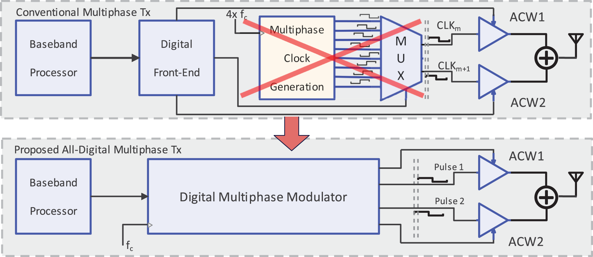
While MP operation reduces the vector-combination power loss, scalability is often limited by the clock subsystem. Generating and distributing  $M$ accurate phases typically requires dedicated circuitry and careful routing, and the burden increases when non- ${50}\%$ duty cycles are required for current-scaling and/or harmonic suppression DTXs [Reference Li, Li, Yin, Yan, Qi, Liu and Xu2, Reference Mul, Bootsman, Beikmirza, Alavi and de Vreede9]. In many MP transmitters, all $M$ phases are distributed continuously even though only a small subset is used for vector synthesis at any instant. Moreover, changing the phase count or duty cycle commonly requires redesign of the local-oscillator (LO) generation and distribution network, as illustrated in Fig. 2.
This paper addresses this bottleneck with a reconfigurable MP modulator that preserves MP vector synthesis while avoiding continuous distribution of  $M$ phase clocks. The basis switching waveforms are reconstructed using a wavetable and a pair of pulse generators. Operating mode is set through wavetable updates, enabling changes in phase count (e.g., MP8–MP16) and duty cycle (e.g., ${50}\%$ and ${33}\%$) without modifying the pulse generator.
An earlier version of this work was presented at EuMW 2025 and published in its proceedings [Reference Sun and Wentzel10]. The present manuscript extends that work by: (1) optimizing the MP8 implementation and updating the corresponding measurements; (2) expanding measurements to 0.9, 2.4, 3.7, and 6 GHz with OFDM bandwidths up to  $500\,\mathrm{MHz}$; (3) demonstrating MP8-to-MP16 scaling via wavetable updates under identical measurement conditions; and (4) introducing and characterizing a six-phase, ${33}\%$ duty cycle harmonic-rejection mode with measured second- and third-harmonic suppression.
Three typical DTX architectures (polar, Cartesian, multiphase) and their operational concepts.

Figure 1 Long description
The image consists of three distinct sections, each representing a different DTX architecture. The first section, labeled Polar TX, includes a sequence of components: a Baseband Unit, a Digital Front-End, a DPLL and a DPA. Arrows indicate the flow of signals, with phi and rho being key parameters. Below this, a grid with circles and axes shows the modulation concept, with phi and rho marked. The second section, labeled Cartesian Tx, features a similar layout with a Baseband Unit, Digital Front-End and DPA, but includes a CLK component. The signal flow is marked by arrows and a grid below illustrates the modulation with axes and a point labeled Q. The third section, labeled Multiphase Tx, includes a Baseband Unit, Digital Front-End, a CLK and a multiplexer with angles from zero to three hundred fifteen degrees. Two DPAs labeled M1 and M2 are connected, with arrows indicating signal paths. Below, a grid with axes shows modulation, with points labeled M1 and M2. Each section visually represents the operational concept of the respective DTX architecture.
Comparison of conventional MP DTXs and the proposed modulator.
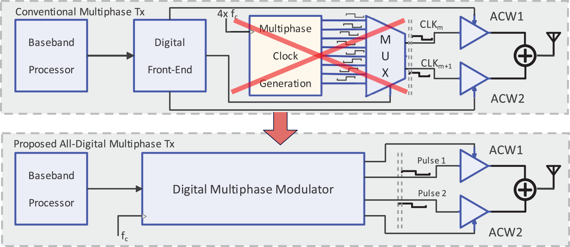
Figure 2 Long description
The diagram consists of two sections comparing conventional and proposed all-digital multiphase transmitters. The top section illustrates the conventional multiphase transmitter. It begins with a baseband processor on the left, connected by an arrow to a digital front-end. From the digital front-end, a line labeled ′4x f subscript c′ leads to a multiphase clock generation block, which is crossed out with a red ′X′. This block connects to a multiplexer labeled ′MUX′, which outputs to two lines labeled ′CLK subscript m′ and ′CLK subscript m plus 1′. These lines connect to two amplifiers labeled ′ACW1′ and ′ACW2′, which are connected to an antenna symbol. The bottom section shows the proposed all-digital multiphase transmitter. It also starts with a baseband processor on the left, connected to a digital multiphase modulator. This modulator outputs two lines labeled ′Pulse 1′ and ′Pulse 2′, which connect to amplifiers labeled ′ACW1′ and ′ACW2′, leading to an antenna symbol. An arrow pointing downward between the two sections indicates the transition from the conventional to the proposed system.
The present work focuses on the modulator architecture and its waveform-level validation. Specifically, the contribution is to demonstrate reconfigurable event-driven synthesis of MP switching waveforms, including phase-count scaling and duty-cycle-controlled harmonic shaping, using a common pulse-generation core. Absolute IC-level power, area, and efficiency benefits are not claimed for the present prototype; instead, these aspects are discussed through a first-order implementation analysis.
The remainder of this paper is organized as follows: Section II introduces the fundamentals of MP modulation and summarizes practical approaches to MP LO generation and distribution. Section III describes the proposed modulator architecture. Section IV discusses implementation considerations and analyzes the robustness of the proposed architecture to timing-related non-idealities. Section V presents experimental results, followed by concluding remarks in Section VI.
MP operation and prior art
Unlike Cartesian transmitters that build the RF vector from orthogonal I/Q bases, an MP-DTX approximates the target vector using several non-orthogonal phase bases around the unit circle, bridging polar and Cartesian concepts. This makes the MP clock one of the most critical blocks in the system, as phase error, skew, and mismatch map directly into spectral degradation. In addition, the phase count must be carefully chosen. More phases give finer constellation approximation and potentially better linearity, but they also tighten phase-matching requirements and increase the burden on the MP clock network (generation, distribution, calibration).
MP vector synthesis and phase-count trade-off
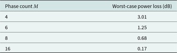
Consider an  $M$-phase architecture with evenly spaced basis vectors separated by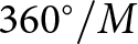 $360^{\circ}/M$. The complex plane is partitioned into $M$ angular sectors. For a target vector within a given sector, the transmitter selects the two adjacent basis vectors that bound that sector and combines them to approximate the desired vector. Table 1 lists the worst-case power loss for adjacent-vector combination versus the phase count $M$. Increasing the phase count reduces the worst-case power loss, but the incremental improvement is limited. In particular, $M=16$ already limits the worst-case power loss to only 0.17 dB, so pushing to phase counts beyond 16 is rarely justified given the added clock-generation/distribution complexity and tighter matching requirements. In practice, $M=8$ is commonly adopted because it offers a good trade-off between loss and hardware cost, and it also enables a simple phase-mapper implementation.
Worst-case vector-synthesis power loss versus phase count

Table 1 Long description
The table reports worst-case vector-synthesis power loss in decibels for different phase counts. At 4 phases, the worst-case loss is 3.01 dB, the highest value listed. Increasing to 6 phases reduces the loss to 1.25 dB, and 8 phases reduces it further to 0.68 dB. At 16 phases, the loss is 0.17 dB, the lowest value in the table. Overall, higher phase counts correspond to lower worst-case power loss, with the largest reduction occurring between 4 and 6 phases. Values are limited to the four phase counts provided, so behavior between these points is not shown.
State-of-the-art MP LO generation and distribution
While MP vector synthesis is conceptually simple, practical DTXs are often limited by generation and distribution of the  $M$-phase LOs. Early MP demonstrations avoided this burden by using externally generated MP clocks; for example, a 16-phase switched-capacitor power amplifier (SCPA) was demonstrated with off-chip clocks [Reference Yuan and Walling8].
Later work integrated MP LO generation on chip. One approach combines polyphase filters (PPFs) with an injection-locked ring oscillator (ILRO) to produce accurate eight-phase clocks [Reference Sheth, Zhang, Shen, Iyer and Bowers1]. The PPF adds matching and buffering overhead, while the ILRO introduces constraints on locking range, spurs, and phase noise as carrier frequency and modulation bandwidth increase.
Another approach derives MP clocks from a higher-frequency reference using flip-flop-based dividers and logic-based duty cycle conditioning [Reference Beikmirza, Shen, de Vreede and Alavi3]. In the reported multimode DTX, the divider requires a  $4f_c$ input clock and additional delay-alignment logic to generate and align the target phases and duty cycles. These schemes are digitally compatible and scalable, but still rely on a high-frequency reference and tight timing alignment across all phases.
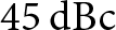
Harmonic-rejection MP DTXs further tighten LO requirements by using duty cycle shaping to suppress specific harmonics. A six-phase harmonic-rejection DTX employs  ${33}\%$ duty cycle LO waveforms that ideally cancel the third harmonic [Reference Li, Li, Yin, Yan, Qi, Liu and Xu2]. Prior results indicate that maintaining third-harmonic rejection (HR3) above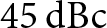 ${45}\,\mathrm{dBc}$ requires duty cycle error below ${0.3}\%$, motivating multiphase injection locking (MPIL) for MP LO generation.
Existing MP LO solutions therefore either rely on external phase generation or use dedicated on-chip MP networks optimized for a fixed phase count and duty cycle. As MP DTXs move toward wider bandwidth and harmonic rejection, the LO subsystem increasingly dominates design effort while offering limited reconfigurability.
Motivation: toward modulator-level reconfigurability
Across prior work, two structural constraints recur:
• Fixed-M and fixed-duty cycle LO networks. The LO generation and distribution network is typically designed for a specific phase count $M$ and a specific duty cycle. Limited multimode support is possible, but changing
$M$ (e.g., MP8–MP16) or duty cycle generally requires redesign of the LO subsystem and its calibration.
$M$ and a specific duty cycle. Limited multimode support is possible, but changing
$M$ (e.g., MP8–MP16) or duty cycle generally requires redesign of the LO subsystem and its calibration.• Always-on generation of many phases despite sparse instantaneous use. In MP operation, only two basis phases contribute at any instant. The remaining phases still must be generated, routed, buffered, and kept accurate, even though they do not contribute to instantaneous output.


These constraints motivate an architectural, modulator-centric approach that reconstructs only the required switching waveforms from scheduled edge events, rather than distributing an always-on  $M$-phase clock network.
Modulator architecture
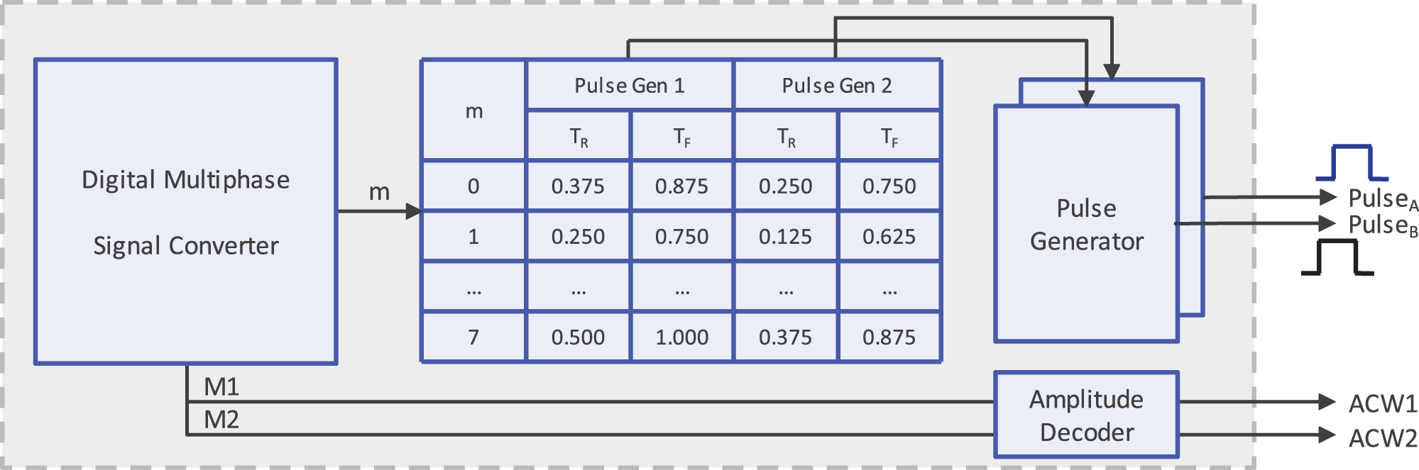
The modulator consists of three blocks: (1) a digital multiphase signal converter (DMSC), (2) a wavetable-based timing controller, and (3) a pulse generator. The system block diagram is shown in Fig. 3.
Digital multiphase signal converter (DMSC)
The DMSC maps the complex baseband sample  $x[n]=I[n]+jQ[n]$ to a phase-sector index $m$ and amplitude control words (ACWs) used for vector synthesis. In contrast to polar conversion, which typically uses CORDIC or large look-up tables (LUTs) to compute magnitude and phase, the DMSC assigns the instantaneous phase $\angle x[n]$ to one of $M$ sectors. For an $M$-phase system, the sector index is
 \begin{equation}
m = \left\lfloor \frac{M}{2\pi}\,\angle\!\big(I[n] + jQ[n]\big) \right\rfloor
\end{equation}
\begin{equation}
m = \left\lfloor \frac{M}{2\pi}\,\angle\!\big(I[n] + jQ[n]\big) \right\rfloor
\end{equation} The index  $m$ addresses the wavetable. In parallel, the DMSC computes the weights for the active basis vectors:
 \begin{equation}
ACW_1 = \frac{I[n] \cdot \sin\left(\frac{2\pi (m+1)}{M}\right) - Q[n] \cdot \cos\left(\frac{2\pi (m+1)}{M}\right)}{\sin\left(\frac{2\pi}{M}\right)}
\end{equation}
\begin{equation}
ACW_1 = \frac{I[n] \cdot \sin\left(\frac{2\pi (m+1)}{M}\right) - Q[n] \cdot \cos\left(\frac{2\pi (m+1)}{M}\right)}{\sin\left(\frac{2\pi}{M}\right)}
\end{equation} \begin{equation}
ACW_2 = \frac{-\left[I[n] \cdot \sin\left(\frac{2\pi m}{M}\right) - Q[n] \cdot \cos\left(\frac{2\pi m}{M}\right)\right]}{\sin\left(\frac{2\pi}{M}\right)}
\end{equation}
\begin{equation}
ACW_2 = \frac{-\left[I[n] \cdot \sin\left(\frac{2\pi m}{M}\right) - Q[n] \cdot \cos\left(\frac{2\pi m}{M}\right)\right]}{\sin\left(\frac{2\pi}{M}\right)}
\end{equation}Block diagram of the proposed modulator architecture. The DMSC maps baseband IQ data to a phase index  $m$, which addresses the wavetable to retrieve normalized edge timing instants ( $T_R, T_F$). These values drive the pulse generators to synthesize the basis waveforms $Pulse_A$ and $Pulse_B$.
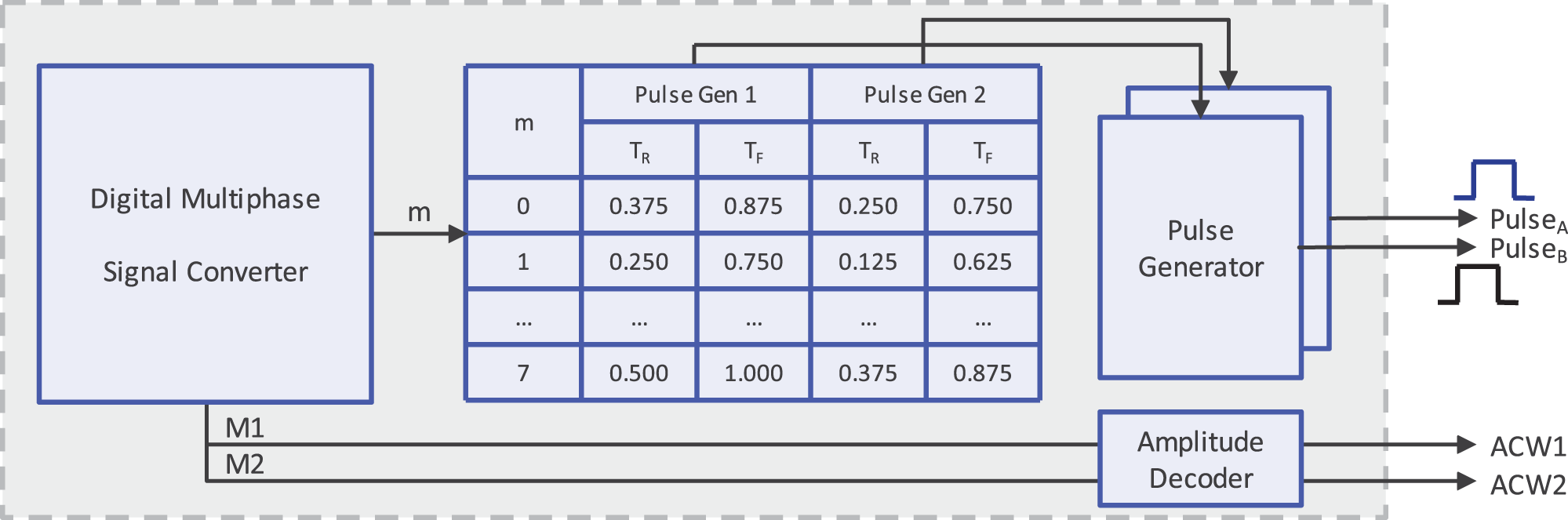
Figure 3 Long description
The diagram illustrates a modulator architecture consisting of several components. On the left, there is a block labeled ′Digital Multiphase Signal Converter′ with an arrow labeled ′m′ pointing to the right. This arrow connects to a table in the center, which is divided into columns labeled ′m′, ′Pulse Gen 1′ and ′Pulse Gen 2′. The ′Pulse Gen 1′ and ′Pulse Gen 2′ columns are further divided into ′T subscript R′ and ′T subscript F′. The table contains rows with values such as 0.375, 0.875, 0.250 and 0.750, corresponding to different ′m′ values ranging from 0 to 7. Arrows from the table lead to a block labeled ′Pulse Generator′ on the right. This block outputs two waveforms labeled ′Pulse subscript A′ and ′Pulse subscript B′. Below the table, two lines labeled ′M1′ and ′M2′ extend to the right, connecting to a block labeled ′Amplitude Decoder′. This block outputs two lines labeled ′ACW1′ and ′ACW2′.
Event-based wavetable
Unlike prior bitstream-based wavetable approaches [Reference Hühn, Wentzel and Heinrich11, Reference Hühn, Wentzel and Heinrich12] that store oversampled sequences and require high readout clock rates, the proposed wavetable stores only the edge times required to reconstruct each basis pulse.
As shown in Fig. 3, each LUT entry is addressed by the sector index  $m$ and stores the normalized rising and falling edge positions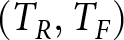 $(T_R,T_F)$ of the basis pulse,
 \begin{equation}
T_R,\;T_F \in [0,1].
\end{equation}
\begin{equation}
T_R,\;T_F \in [0,1].
\end{equation} Reconfiguration is achieved by updating 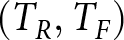 $(T_R,T_F)$ to modify the duty cycle and relative phase offsets. Static timing offsets in the edge-generation paths, such as rise/fall skew or per-phase delay mismatch, can in principle be pre-compensated by adjusting the stored edge positions after pulse-generator characterization. Phase-count scaling is then realized by updating the wavetable entries and the DMSC phase-sector parameter $M$, while leaving the pulse-generator hardware unchanged.
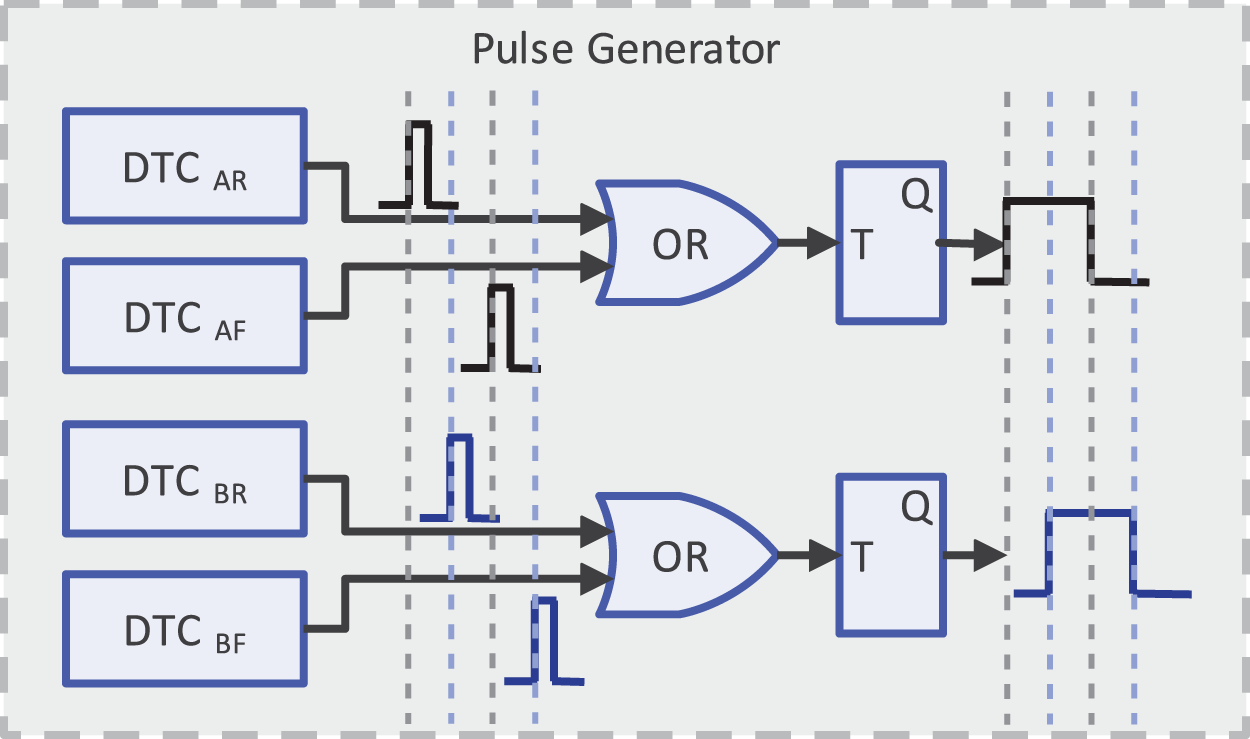
Conceptual pulse generator. Independent DTCs position the rising ( $T_R$) and falling ( $T_F$) edges. The resulting triggers are logically OR’d to toggle a T flip-flop.

Pulse generator
Figure 4 illustrates one possible circuit-level realization of the proposed pulse generator. The logic is based on [Reference Lemberg, Kosunen, Roverato, Martelius, Stadius, Anttila, Valkama and Ryynänen13] and adapted here for wavetable-driven operation. Timing granularity, and therefore the achievable phase and duty-cycle resolution, is set by the DTC resolution.
A single reference clock at  $f_c$ defines the timing reference for each carrier period. Reconstruction of one basis waveform (e.g., $Pulse_A$) uses two parallel DTC paths driven by the programmed edge times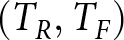 $(T_R,T_F)$ obtained from the wavetable. One path positions the rising transition and the other positions the falling transition. The two trigger pulses are combined by a logical OR to form the composite trigger $OR_A$, which clocks a toggle flip-flop (T-FF). The first trigger sets $Pulse_A$ high and the second returns it low, so that the resulting duty cycle is
 \begin{equation}
T_{\mathrm{dc}} = T_F - T_R .
\end{equation}
\begin{equation}
T_{\mathrm{dc}} = T_F - T_R .
\end{equation}Implementation considerations and robustness analysis
Edge-timing error definitions
Each basis waveform is defined by two programmed edge instants within one carrier period  $T_c$. Let the ideal rising and falling edge times be $T_R$ and $T_F$, and the realized edges be
 \begin{equation}
T_R' = T_R + \Delta T_R,\qquad
T_F' = T_F + \Delta T_F .
\end{equation}
\begin{equation}
T_R' = T_R + \Delta T_R,\qquad
T_F' = T_F + \Delta T_F .
\end{equation}The resulting duty-cycle error is
 \begin{equation}
\varepsilon = (T_F' - T_R') - (T_F - T_R) = \Delta T_F - \Delta T_R .
\end{equation}
\begin{equation}
\varepsilon = (T_F' - T_R') - (T_F - T_R) = \Delta T_F - \Delta T_R .
\end{equation}Therefore, duty-cycle error is set by the differential edge error, whereas a common shift of both edges primarily perturbs pulse timing and, ideally, does not change the duty cycle.
Short-duty-cycle operation imposes additional constraints on the timing front-end. As the target duty cycle decreases, the programmed edge events move closer together, reducing the guard interval available to generate two distinct trigger pulses. The DTC must therefore produce pulses that are short enough to avoid overlap while still satisfying the minimum pulse-width requirement of the subsequent clock path. Practical limits arise from the T-FF input pulse-width requirement and from possible pulse suppression in the combining logic, for example, due to inertial delay or glitch filtering. These constraints become more severe as  $f_c$ increases, since the carrier period $T_c$ decreases while timing uncertainty, such as DTC jitter and nonlinearity, does not scale with $T_c$.
In the  ${50}\%$ duty-cycle modes, edge-placement errors degrade ACLR and EVM through vector-synthesis error. In the ${33}\%$ duty-cycle harmonic-rejection mode, duty-cycle accuracy directly determines the achievable harmonic suppression and is therefore more sensitive to $\varepsilon$.
The next subsection evaluates these sensitivities by behavioral simulation.
Behavioral robustness to timing errors
Behavioral simulations were performed to assess the sensitivity of the proposed architecture to edge-timing uncertainty in both the  ${33}\%$ duty-cycle harmonic-rejection mode and the MP8, ${50}\%$ duty-cycle mode.
For the  ${33}\%$ duty-cycle mode, harmonic rejection is directly determined by duty-cycle accuracy. Using the differential edge-error definition
 \begin{equation}
\Delta t_{\Delta} \triangleq \Delta T_F - \Delta T_R ,
\end{equation}
\begin{equation}
\Delta t_{\Delta} \triangleq \Delta T_F - \Delta T_R ,
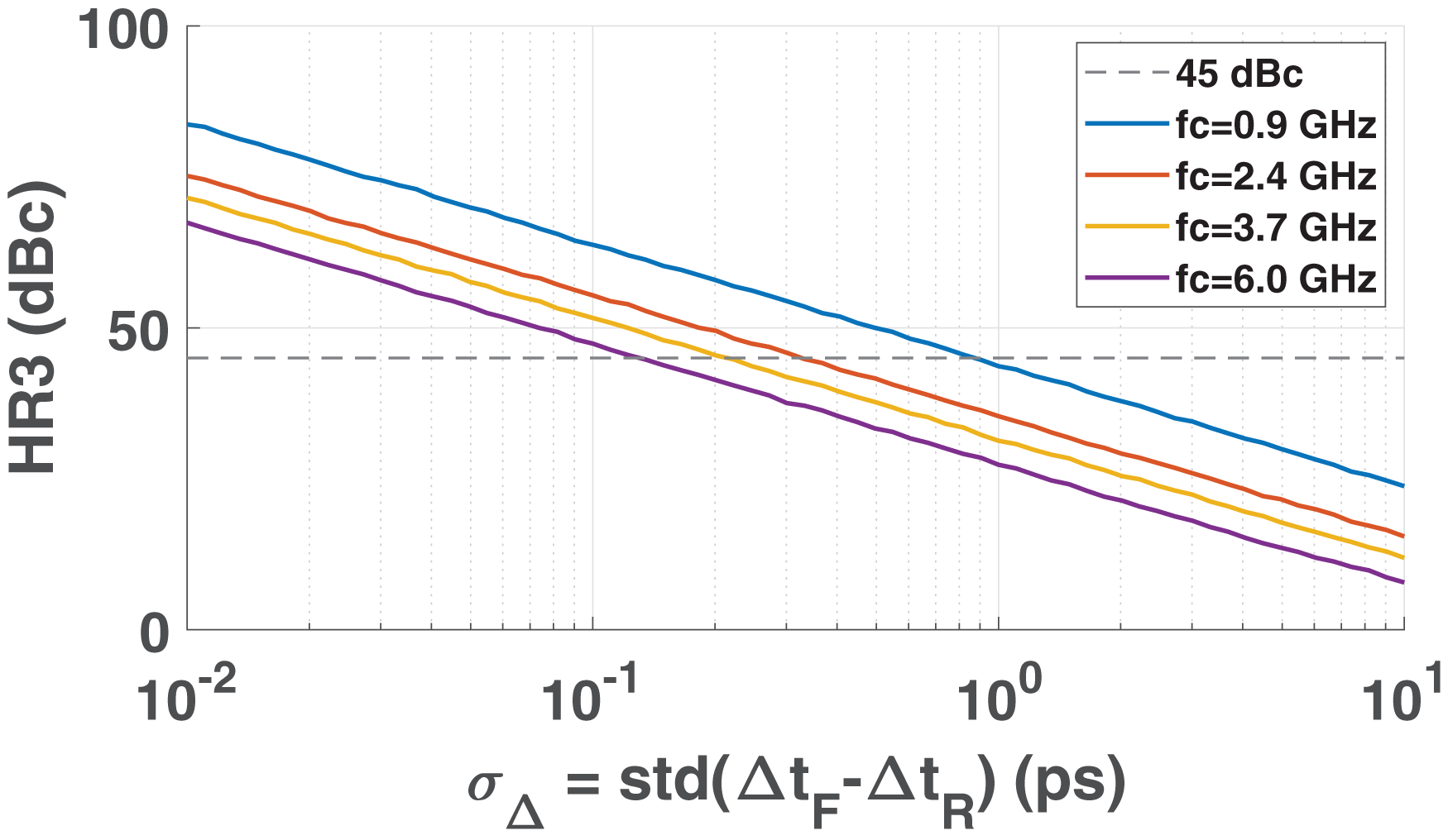
\end{equation} Monte Carlo simulations ( $N_\mathrm{MC}=5000$) were carried out on a periodic pulse train. Figure 5 shows the 5th-percentile HR3 versus $\sigma_{\Delta}=\mathrm{std}(\Delta t_{\Delta})$ for carrier frequencies from 0.9–6.0 GHz. HR3 decreases with increasing $\sigma_{\Delta}$, and the degradation is more severe at higher $f_c$ because the same absolute edge error occupies a larger fraction of the carrier period $T_c$.
Simulated 5th-percentile HR3 versus differential edge-error standard deviation  $\sigma_{\Delta}=\mathrm{std}(\Delta T_F-\Delta T_R)$ for a ${33}\%$ duty cycle pulse train.

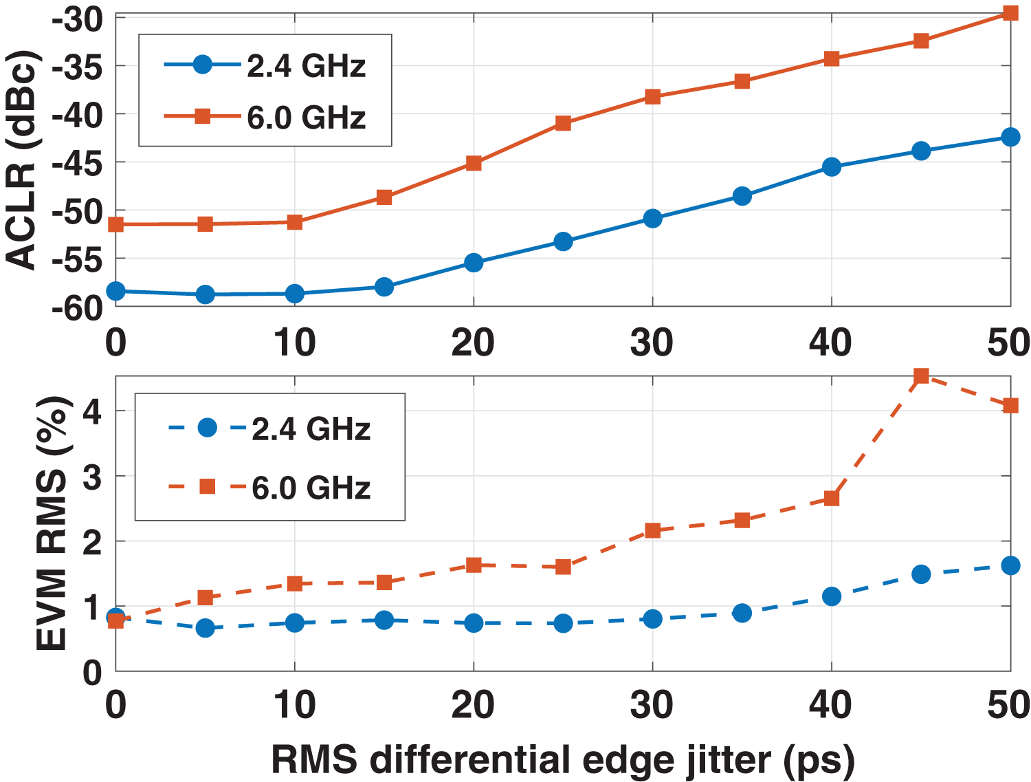
Simulated sensitivity of (top) ACLR and (bottom)  $\text{EVM}_{\text{rms}}$ to rms differential edge jitter for the MP8 transmitter in the 50% duty-cycle mode, using a 20-MHz OFDM signal with 9-dB PAPR at $f_c={2.4}\,\mathrm{GHz}$ and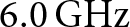 ${6.0}\,\mathrm{GHz}$.

Figure 6 Long description
A) A line graph with the vertical axis labeled ACLR (dBc) and tick labels negative 60, negative 55, negative 50, negative 45, negative 40, negative 35, negative 30. The horizontal axis shows tick labels 0, 10, 20, 30, 40, 50. A legend lists 2.4 GHz and 6.0 GHz. The 2.4 GHz series has markers at 0: about negative 59; 5: about negative 59; 10: about negative 59; 15: about negative 58; 20: about negative 55; 25: about negative 53; 30: about negative 51; 35: about negative 49; 40: about negative 46; 45: about negative 44; 50: about negative 43. The 6.0 GHz series has markers at 0: about negative 51; 5: about negative 51; 10: about negative 51; 15: about negative 49; 20: about negative 45; 25: about negative 41; 30: about negative 38; 35: about negative 37; 40: about negative 35; 45: about negative 33; 50: about negative 30. B) A line graph with the vertical axis labeled EVM RMS (percent) and tick labels 0, 1, 2, 3, 4. The horizontal axis is labeled RMS differential edge jitter (ps) with tick labels 0, 10, 20, 30, 40, 50. A legend lists 2.4 GHz and 6.0 GHz. The 2.4 GHz series has markers at 0: about 0.8; 5: about 0.7; 10: about 0.8; 15: about 0.8; 20: about 0.8; 25: about 0.8; 30: about 0.85; 35: about 0.9; 40: about 1.2; 45: about 1.5; 50: about 1.6. The 6.0 GHz series has markers at 0: about 0.8; 5: about 1.1; 10: about 1.3; 15: about 1.35; 20: about 1.6; 25: about 1.6; 30: about 2.2; 35: about 2.3; 40: about 2.6; 45: about 4.5; 50: about 4.1.
Figure 6 shows the simulated ACLR and  $\text{EVM}_{\text{rms}}$ versus the rms differential edge jitter added to both pulse generators for the MP8 50% duty-cycle mode, using a 20-MHz OFDM signal with a 9-dB PAPR. As the carrier frequency increases from 2.4 to 6.0 GHz, the sensitivity to differential edge jitter becomes more pronounced. However, even at 6.0 GHz, jitter below approximately 15 ps results in only modest degradation, indicating that good spectral performance is preserved in this range.
While detailed DNL/INL modeling is deferred to future work, static DTC non-linearities would manifest as deterministic phase offsets and duty-cycle skew. However, these static errors could, in principle, be mitigated in the proposed wavetable architecture by pre-compensating the stored edge values.
First-order implementation comparison
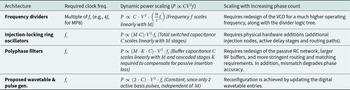
Because no integrated circuit implementation is presented here, absolute power and area estimates would be strongly technology- and layout-dependent. Table 2 therefore provides a first-order comparison between the proposed event-driven modulator and representative conventional MP generation approaches. As the supported phase count M increases, conventional MP implementations generally require higher clock-generation, routing, and buffering overhead. By contrast, the proposed wavetable-based architecture reconstructs only the basis pulses required for the selected vector synthesis, thereby shifting the phase-scaling burden primarily to the digital domain. As a result, the RF clock-generation and distribution overhead remains largely insensitive to phase count, provided that the number of simultaneously active basis-pulse paths remains unchanged.
First-order complexity and scaling comparison of multiphase generation architectures
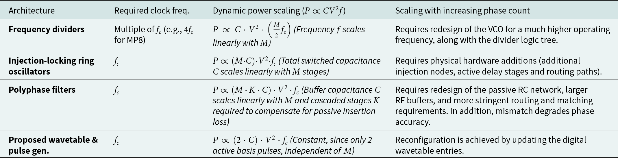
Table 2 Long description
The table compares four multiphase generation architectures by required clock frequency, how dynamic power grows with added phases, and what changes are needed when phase count increases. Frequency dividers need a clock that is a multiple of the carrier, so power rises because switching frequency increases with phase count, and scaling requires redesigning the oscillator for much higher speed plus a larger divider tree. Injection-locking ring oscillators run at the carrier frequency, but power increases because total switched capacitance grows with the number of stages, and scaling needs added injection nodes, delay stages, and routing. Polyphase filters also run at the carrier frequency, but power grows with both the number of phases and the number of cascaded stages needed to offset passive loss, and scaling requires redesigning the passive network, larger buffers, tighter routing and matching, with mismatch reducing phase accuracy. The proposed wavetable and pulse generator runs at the carrier frequency and keeps dynamic power roughly constant because it uses only two active basis pulses regardless of phase count. Its scaling is mainly a digital update to wavetable entries rather than adding or redesigning analog hardware. Power comparisons are qualitative and focus on switching-related trends, not absolute measured values.
Experimental results
Measurement setup and test conditions
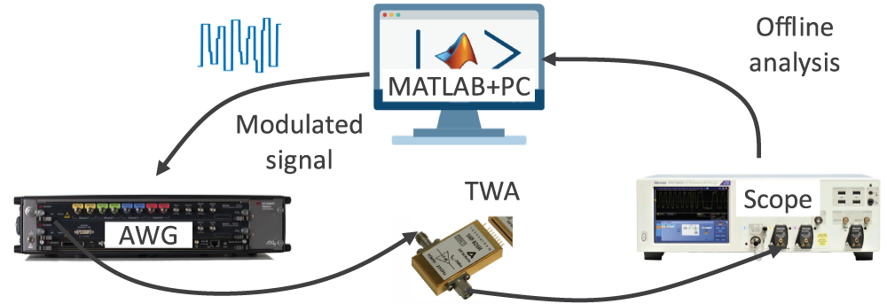
The reconfigurable MP modulator is implemented in MATLAB, and the resulting RF waveform is uploaded to and played back by a Keysight M8195A arbitrary waveform generator (AWG). The AWG output is amplified using an SHF 824 broadband traveling-wave amplifier (TWA), and subsequently captured using a Tektronix DPO 77002SX real-time oscilloscope (see Fig. 7). ACLR and EVM are computed offline in MATLAB from the recorded waveform. The reported average output power  $P_{\mathrm{out}}$ is referenced to the TWA output. The TWA is used here to emulate a digital PA; accordingly, this work reports linearity and delivered output power and does not evaluate efficiency. The RF waveforms are generated by the AWG (8bit vertical resolution and up to 65GSa/s sampling, i.e., $\approx {16}\,\mathrm{ps}$ sample interval). The measurement setup validates the proposed modulator under practical instrument limitations, including AWG quantization and sampling discretization. Accordingly, the measurements should be interpreted as a waveform-level validation of the proposed modulation principle and its reconfigurability, rather than as a full integrated-transmitter demonstration. The impact of integrated edge-generation nonidealities (e.g., DNL/INL) is outside the scope of this work and will be addressed in future work.
Measurement setup.

MP8/MP16 operation with
${50}\%$ duty cycle

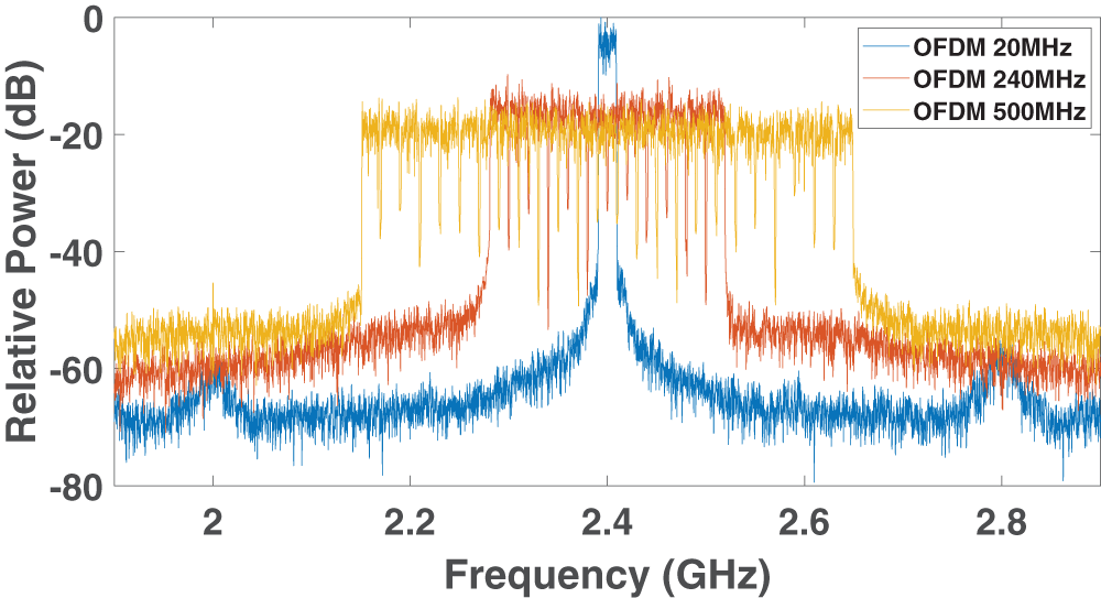
MP8 operation with  ${50}\%$ duty cycle is used as the reference to demonstrate wideband operation and intrinsic modulator linearity. Measurements are reported at carrier frequencies of 0.9, 2.4, 3.7, and 6 GHz. Three OFDM baseband signals are used with occupied bandwidths of ${20}\,\mathrm{MHz}$, ${240}\,\mathrm{MHz}$, and ${500}\,\mathrm{MHz}$. The corresponding PAPR is approximately 9–10 dB, as indicated in the signal labels. A representative measured spectrum for these signals at $f_c={2.4} GHz$ is shown in Fig. 8.
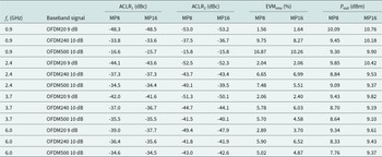
Table 3 summarizes ACLR,  $\text{EVM}_{\text{rms}}$, and delivered output power for MP8 and MP16 across carrier frequency and signal bandwidth. With OFDM20, MP8 achieves ACLR $_2$ better than ${-48}\,\mathrm{dBc}$ and $\text{EVM}_{\text{rms}}$ of ${1.6}\% \mathrm{to} {2.9}\%$ over 0.9–6 GHz. With OFDM240 and OFDM500, the worst-case ACLR $_1$ remains ${-34}\,\mathrm{dBc}$ over 2.4–6 GHz, with $\text{EVM}_{\text{rms}}$ of approximately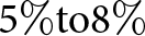 ${5}\% \mathrm{to} {8}\%$. This trend is consistent with the previously noted AWG discretization limits: as $f_c$ increases, the effect of limited AWG sample interval and amplitude resolution becomes more significant.
Measured spectrum at  $f_c={2.4} GHz$ for MP8 with ${50}\%$ duty cycle using OFDM signals.

Measured performance of the proposed modulator in MP8/MP16 modes (50% duty cycle) using OFDM waveforms
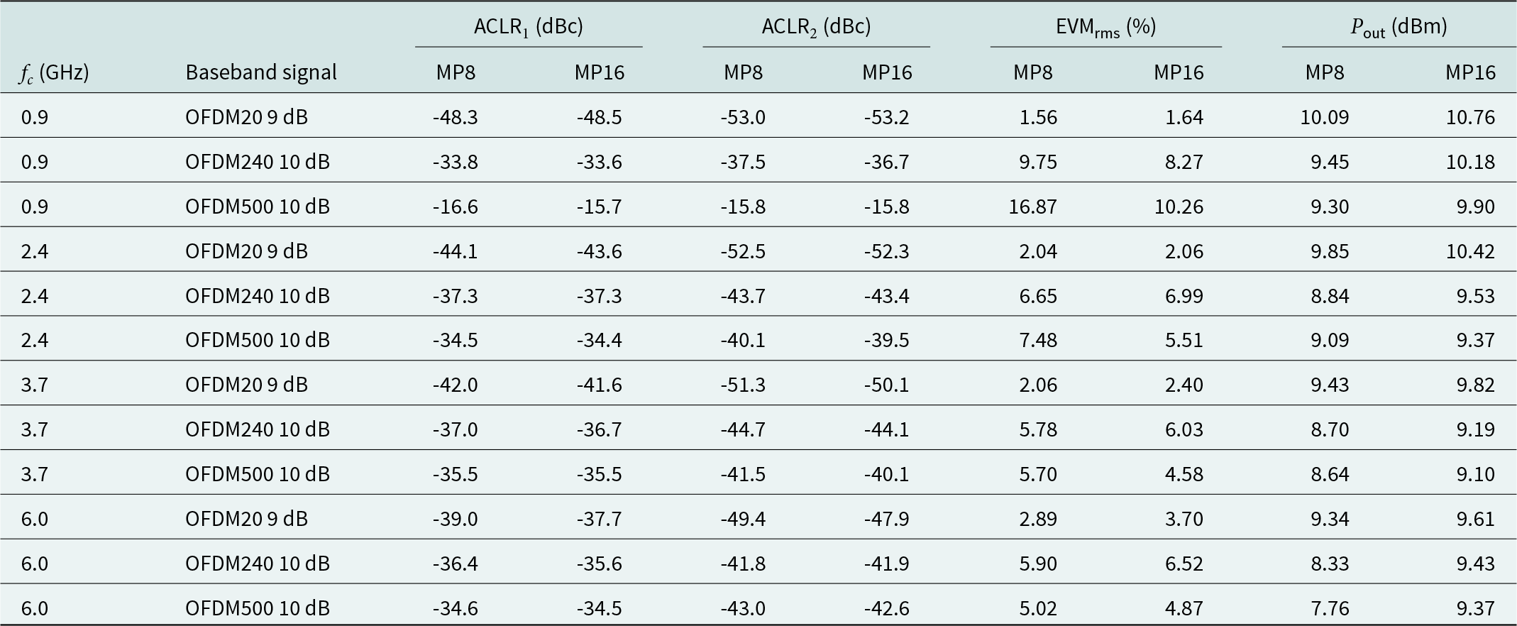
Table 3 Long description
The table reports measured adjacent channel leakage ratios, root mean square error vector magnitude, and output power for a modulator operating in MP8 and MP16 modes at four carrier frequencies and three OFDM bandwidth and backoff settings. For the narrowest waveform (OFDM20 with 9 dB backoff), adjacent channel leakage is strongest, around minus 39 to minus 48 dBc for the first offset and around minus 48 to minus 53 dBc for the second offset, with low error vector magnitude near 1.6 to 3.7 percent and output power around 9.3 to 10.8 dBm. For OFDM240 with 10 dB backoff, leakage is moderate, roughly minus 33.6 to minus 37.3 dBc for the first offset and minus 36.7 to minus 44.7 dBc for the second, with error vector magnitude about 5.8 to 9.8 percent and output power about 8.3 to 10.2 dBm. For the widest waveform (OFDM500 with 10 dB backoff), leakage generally degrades and error vector magnitude rises, including the poorest case at 0.9 GHz where leakage is about minus 16 dBc and error vector magnitude reaches about 16.9 percent, while output power remains near 8.6 to 9.9 dBm. MP8 and MP16 are usually close in leakage and output power, but error vector magnitude can differ by several percentage points depending on frequency and waveform, with MP16 sometimes lower and sometimes higher. Overall, output power stays fairly stable across frequency, while spectral leakage and modulation quality are driven more by waveform bandwidth and operating point than by carrier frequency. Leakage values are reported as averages across the lower and upper adjacent sidebands.
ACLR $_1$ and ACLR $_2$ are averaged between lower and upper sidebands.
Reconfigurability in phase count is demonstrated by enlarging the wavetable while reusing the same pulse generator and measurement setup. As summarized in Table 3, MP16 delivers higher  $P_{\mathrm{out}}$ than MP8 at all 12 measured cases. The delivered-power increase is 0.66 dB on average (median 0.59 dB), ranging from 0.27 dB (OFDM20 at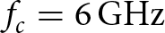 $f_c={6}\,\mathrm{GHz}$) to 1.61 dB (OFDM500 at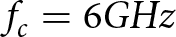 $f_c={6} {GHz}$). This trend follows the reduced vector-combination power loss expected with higher phase resolution.
Spectral performance remains comparable. ACLR typically changes by less than 1 dB from MP8 to MP16; the largest deviations are 1.3 dB for ACLR $_1$ and 1.5 dB for ACLR $_2$ (both for OFDM20 at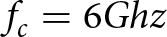 $f_c={6} {Ghz}$). $\text{EVM}_{\text{rms}}$ is also preserved: the absolute change is within ${1}\%$ for most cases, and several wideband cases improve under MP16.
Overall, both MP8 and MP16 exhibit good linearity over the measured operating range, as indicated by limited spectral regrowth.
Harmonic-rejection mode: MP6 with
${33}\%$ duty cycle

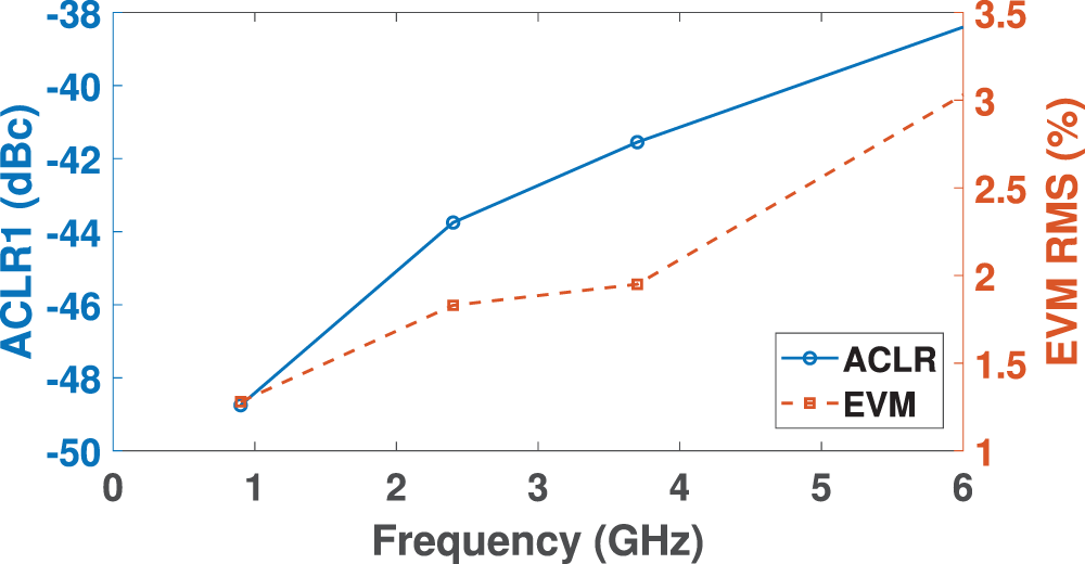
An MP6 harmonic-rejection mode is evaluated to quantify harmonic suppression. In this mode, the wavetable specifies six  ${33}\%$ duty cycle basis pulses. With OFDM20 over 0.9–6 GHz, MP6 maintains spectral performance (see Fig. 9) comparable to the MP8 reference (see Table 3). $\text{EVM}_{\text{rms}}$ remains below ${3.1}\%$ at all carrier frequencies, indicating that the reduced phase count and modified duty cycle do not degrade spectral linearity in this mode.
Measured ACLR and EVM for OFDM20 across carrier frequency using the MP6 with  ${33}\%$ duty cycle.

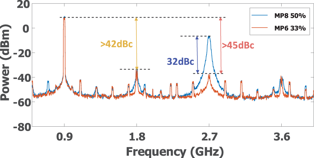
Figure 10 shows far-out spectra for OFDM20 at  $f_c={0.9}\,\mathrm{Ghz}$, comparing MP6 with the ${50}\%$ duty cycle MP8 reference. Under the same measurement conditions, MP8 exhibits substantially higher harmonic levels, MP6 achieves approximately ${42}\,\mathrm{dBc}$ and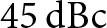 ${45}\,\mathrm{dBc}$ rejection of the second and third harmonics, respectively, demonstrating that duty cycle shaping implemented via wavetable provides good suppression. Because DPAs are typically implemented with differential outputs, the even-order harmonics generated at the two terminals largely cancel when combined, so the third-harmonic improvement at $3f_c$ is the more critical benefit of the ${33}\%$ duty cycle mode.
Far-out measured spectrum for OFDM20 at 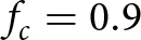 $f_c=0.9$ GHz.

Figure 10 Long description
Power (decibel milliwatt) versus Frequency (gigahertz). The x-axis is labeled Frequency (gigahertz), with labeled ticks at 0.9, 1.8, 2.7 and 3.6. The y-axis is labeled Power (decibel milliwatt), ranging from minus 80 to 20, with labeled ticks at minus 80, minus 60, minus 40, minus 20, 0 and 20. A legend in the upper right lists two line series: MP8 50 percent and MP6 33 percent. Both series show a tall narrow peak near the 0.9 tick, reaching slightly above 0 on the power scale. Across the full frequency range, both series show multiple smaller narrow peaks on a baseline around minus 60 to minus 50. Near the 1.8 tick, a narrow peak is marked with a vertical arrow labeled greater than 42 decibel relative to carrier, spanning between two dashed horizontal reference lines. Near the 2.7 tick, a broader peak is marked with a vertical arrow labeled 32 decibel relative to carrier, spanning between two dashed horizontal reference lines. Near the right side of the 2.7 region, another vertical arrow is labeled greater than 45 decibel relative to carrier, spanning between two dashed horizontal reference lines.
In particular, the fifth harmonic is not cancelled by the  ${33}\%$ duty cycle condition. In practice, however, $5f_c$ is farther from the desired band than $2f_c$ and $3f_c$, so conventional band-pass or low-pass output filtering typically provides substantially higher attenuation at $5f_c$. As a result, the MP6 mode primarily relaxes the most demanding portion of the filter requirement, while residual higher-order harmonics are handled by the output filter.
Conclusion
This paper presented a reconfigurable wavetable-based MP RF modulator that reconstructs its switching waveforms with an event-driven pulse generator, thereby avoiding continuous MP LO distribution in the modulator path. A waveform-level proof-of-concept transmitter chain was demonstrated from 0.9 GHz to 6 GHz using OFDM bandwidths up to 500 MHz. For an OFDM20 signal, the measured ACLR reaches  ${-48.3}\,\mathrm{dBc}$ at $f_c={0.9} GHz$ and remains ${-39}\,\mathrm{dBc}$ up to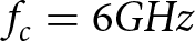 $f_c={6} GHz$. For wideband OFDM500 operation over
 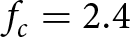 $f_c=
2.4$–6.0 GHz, ACLR stays better than
$f_c=
2.4$–6.0 GHz, ACLR stays better than  ${-34.6}\,\mathrm{dBc}$. Simple wavetable updates support scaling from MP8 to MP16, yielding up to 1.61 dB higher delivered output power, and enable a ${33}\%$-duty MP6 harmonic-rejection mode with about ${42}\,\mathrm{dBc}/{45}\,\mathrm{dBc}$ second-/third-harmonic suppression, all while maintaining comparable ACLR and EVM. These results demonstrate a modulator concept for future wideband all-digital MP transmitters.
Funding statement
This project was supported by the Deutsche Forschungsgemeinschaft (DFG) under grant no. WE6288/10-1 / GE 2848/11, which is gratefully acknowledged. Furthermore, this work was partly funded by German Federal Ministry of Research, Technology and Space (BMFTR) within the project “GreenICT@FMD” under ref. 16ME0505.
Competing interests
The authors declare none.

Deguang Sun (Student Member, IEEE) received the B.Eng. degree in communication engineering from Hainan University, China, in 2020, and the M.Sc. degree in signal processing from Nanyang Technological University, Singapore, in 2022. He is currently a research assistant with the Ferdinand-Braun-Institut (FBH), Germany. His research interests include signal processing for efficient all-digital transmitters and RF modulators.

Andreas Wentzel (M‘16) received the Diploma and the Doctoral degree in electrical engineering from the Technical University of Berlin, Germany, in 2006 and 2011, respectively. Since 2015, he has been the head of the Digital PA Lab in the III-V-Electronics department of the Ferdinand- Braun-Institut in Berlin, Germany. His research activities focus on the design, realization, and measurements of flexible digital TX architectures including advanced switch-mode power amplifier concepts realized on GaN and InP from GHz to sub-THz as well as on optimized modulation schemes suitable for these types of PAs. Moreover, his focus is on GaN- and AlN-based highly-efficient VHF power converters up to GHz-range. Dr. Wentzel is a member of IEEE and MTT society.













 Open access

