




I. ISSUES WITH Si-MOSFET AND THE ADVANTAGE OF 2D CHANNELS
The issues with the miniaturization of Si-MOSFETs are generically called short channel effects.
Reference Sze and Ng1
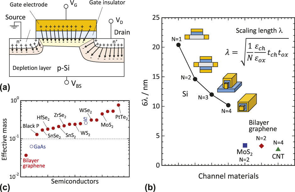
When the source and drain depletion regions become comparable in length with the channel length, as shown in Fig. 1(a), the drain bias weakens the gate bias, which leads to a drastic increase in the off-current. Based on an analysis of the distribution of the electrical potential in the channel region, it is widely known that the short channel effect can be neglected when the channel length is ∼6 times longer than the scaling length, $\lambda = \sqrt {\left( {{\varepsilon _{{\rm{ch}}}}{t_{{\rm{ch}}}}{t_{{\rm{ox}}}}} \right)/\left( {N{\varepsilon _{{\rm{ox}}}}} \right)}$
,
Reference Ferain, Colinge and Colinge2,Reference Yan, Ourmazd and Lee3
where εch, εox, t
ch, and t
ox are the dielectric constants for the channel, the gate insulator, the thickness of the channel, and the gate oxide, respectively. Figure 1(b) shows the 6λ values calculated for Si, carbon nanotubes (CNT), bilayer graphene, and MoS2, where the contribution of the tunneling effect is neglected. N is defined as the effective gate number: N = 1 for planar, N = 2 for dual gate, N = 3 for FIN-FET, and N = 4 for gate-all-around. Although the FIN structure has already been adopted for Si to reduce the short channel effects,
Reference Bohr4
it is difficult to avoid the short channel effects for channel lengths shorter than 10 nm. 2D layered channels in FET applications are attractive because of their rigidly controllable atomic thickness (t
ch < 1 nm) and their low dielectric constants where εch = ∼4 for a typical 2D layered channel.
Reference Yan, Ourmazd and Lee3,Reference Bohr4
This results in a 6λ smaller than that of Si. Of course, Si channels of a few nanometers thick have already been constructed using the microfabrication process. However, the operation of Si-MOSFET with an atomic scale thickness is not realistic because the mobility is drastically reduced because of fabrication damage.
Reference Gomez, Aberg and Hoyt5,Reference Granzner, Polyakov, Schippel and Schwierz6
The advantage of 2D materials is their intrinsic atomic thickness,
Reference Schwierz7,Reference Butler, Hollen, Cao, Cui, Gupta, Gutiérrez, Heinz, Hong, Huang, Ismach, Johnston-Halperin, Kuno, Plashnitsa, Robinson, Ruoff, Salahuddin, Shan, Shi, Spencer, Terrones, Windl and Goldberger8
which allows both the reduction of the short channel effect and the possible retention of high mobility. For the short channel devices in which quasiballistic transport is assumed, the on-current can be determined not by the mobility but by the effective mass. Figure 1(c) shows effective masses (m*) for 2D materials.
Reference Zhang, Huang, Zhang and Li9
Although there are many 2D channels, bilayer graphene has the lowest effective mass. Therefore, bilayer graphene with an electrostatically tunable band gap still has an advantage over the high performance device.
$\lambda = \sqrt {\left( {{\varepsilon _{{\rm{ch}}}}{t_{{\rm{ch}}}}{t_{{\rm{ox}}}}} \right)/\left( {N{\varepsilon _{{\rm{ox}}}}} \right)}$
,
Reference Ferain, Colinge and Colinge2,Reference Yan, Ourmazd and Lee3
where εch, εox, t
ch, and t
ox are the dielectric constants for the channel, the gate insulator, the thickness of the channel, and the gate oxide, respectively. Figure 1(b) shows the 6λ values calculated for Si, carbon nanotubes (CNT), bilayer graphene, and MoS2, where the contribution of the tunneling effect is neglected. N is defined as the effective gate number: N = 1 for planar, N = 2 for dual gate, N = 3 for FIN-FET, and N = 4 for gate-all-around. Although the FIN structure has already been adopted for Si to reduce the short channel effects,
Reference Bohr4
it is difficult to avoid the short channel effects for channel lengths shorter than 10 nm. 2D layered channels in FET applications are attractive because of their rigidly controllable atomic thickness (t
ch < 1 nm) and their low dielectric constants where εch = ∼4 for a typical 2D layered channel.
Reference Yan, Ourmazd and Lee3,Reference Bohr4
This results in a 6λ smaller than that of Si. Of course, Si channels of a few nanometers thick have already been constructed using the microfabrication process. However, the operation of Si-MOSFET with an atomic scale thickness is not realistic because the mobility is drastically reduced because of fabrication damage.
Reference Gomez, Aberg and Hoyt5,Reference Granzner, Polyakov, Schippel and Schwierz6
The advantage of 2D materials is their intrinsic atomic thickness,
Reference Schwierz7,Reference Butler, Hollen, Cao, Cui, Gupta, Gutiérrez, Heinz, Hong, Huang, Ismach, Johnston-Halperin, Kuno, Plashnitsa, Robinson, Ruoff, Salahuddin, Shan, Shi, Spencer, Terrones, Windl and Goldberger8
which allows both the reduction of the short channel effect and the possible retention of high mobility. For the short channel devices in which quasiballistic transport is assumed, the on-current can be determined not by the mobility but by the effective mass. Figure 1(c) shows effective masses (m*) for 2D materials.
Reference Zhang, Huang, Zhang and Li9
Although there are many 2D channels, bilayer graphene has the lowest effective mass. Therefore, bilayer graphene with an electrostatically tunable band gap still has an advantage over the high performance device.
(a) The charge conservation model for Si-MOSFETs. Reference Sze and Ng1 (b) 6λ for Si, CNT, bilayer graphene and MoS2. t ch = 5 nm for Si, and t ch = 1 nm for all other channel materials. Although Poisson's equation in cylindrical co-ordinates should be solved for CNT, the present expression (N = 4) was used for simplicity. (c) Electron effective mass for 2D materials. Reference Zhang, Huang, Zhang and Li9
II. GATE STACK FORMATION FOR 2D CHANNELS
One of the most important building blocks for an FET is the gate stack formation because the device performance is mainly controlled by the carriers that flow near the channel/insulator interface. This is especially true of graphene, which has an atomic monolayer composed of a strong sp 2 hybrid orbital. The defects introduced in graphene during the top gate insulator formation results in the severe degradation of the electron transport properties. Many deposition methods were tested during the initial stages of graphene gate stack research. Reference Ni, Wang, Kasim, Wu and Shen10 The obstacles specific to each deposition method have been elucidated. Physical vapor deposition (PVD) methods using high particle energy, such as radio frequency sputtering Reference Ni, Wang, Kasim, Wu and Shen10,Reference Jin, Su, Chen, Liu and Wu11 and pulsed laser deposition, Reference Ni, Wang, Kasim, Wu and Shen10 introduce a significant amount of defects in graphene. Most of the deposition techniques applicable to the conventional Si process are not applicable to graphene. On the other hand, atomic layer deposition (ALD) Reference Wang, Tabakman and Dai12 has difficulties with nucleation because the graphene surface is chemically inert. Therefore, as shown in Fig. 2(a), Y2O3 is deposited only on defects and grain boundaries in highly oriented pyrolytic graphite (HOPG) by ALD. These issues have been overcome by the utilization of PVD Reference Wang, Xu, Zhang, Wnag, Ding, Zeng, Yang, Pei, Liang, Gao and Peng13–Reference Nagashio, Nishimura and Toriumi16 with particle energies lower than that required to displace one C atom out of graphene [∼7.5 eV (Refs. Reference Chen, Casu, Gajek and Raoux17 and Reference Lehtinen, Kotakoski, Krasheninnikov and Keinonen18)] and by the utilization of buffer layers such as thin oxidized metal layers, Reference Kim, Nah, Jo, Shahrjerdi, Colombo, Yao, Tutuc and Banerjee19 polymer coating, Reference Farmer, Chiu, Lin, Jenkins, Xia and Avouris20 or other types of materials Reference Wang, Tabakman and Dai12,Reference Williams, DiCarlo and Marcus21–Reference Jandhyala, Mordi, Lee, Lee, Floresca, Cha, Ahn, Wallace, Chabal, Kim, Colombo, Cho and Kim23 for ALD. In this case, no defect is introduced. Interestingly, as shown in Fig. 2(b), Y2O3 was deposited directly on approximately 70% of the h-BN surface without any preferences for the grain boundaries or defects due to the physical adsorption of the Y precursor from the polarization in h-BN. This is the big difference between graphene and other compound type 2D materials. Further utilization of a buffer layer results in the full surface coverage of ALD-Y2O3 with a small surface roughness of approximately 0.2 nm, as shown in Fig. 2(c). Reference Takahashi, Watanabe, Taniguchi and Nagashio24
AFM images for (a) Y2O3 on HOPG, (b) Y2O3 on h-BN, and (c) Y2O3 on h-BN with an oxidized Y metal buffer layer of 1.5 nm. The bottom figures show the relative height profiles along the dotted lines in the AFM images.

Using an alternative technique to ALD, we have succeeded the high insulating properties of high-k Y2O3 top-gate in graphene FETs by depositing Y metal in an O2 atmosphere and subsequently applying high-pressure O2 annealing (100 atm).
Reference Kanayama, Nagashio, Nishimura and Toriumi25
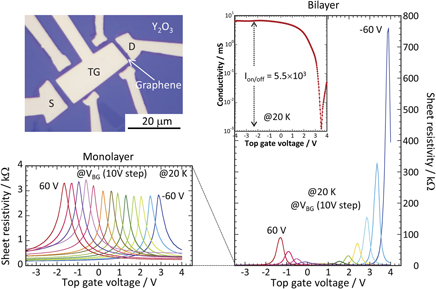
Y metal was selected because it has the highest susceptibility to oxidation given the thermodynamic considerations. Figure 3 shows the sheet resistivity of monolayer and bilayer graphene as a function of top gate voltage (V
TG) for different back gate voltages (V
BG), respectively.
Reference Kanayama, Nagashio, Nishimura and Toriumi25,Reference Kanayama and Nagashio26
These devices were fabricated on SiO2 (∼90 nm)/n
+-Si substrates by the mechanical exfoliation of Kish graphite. For monolayer graphene, as expected from the linear dispersion without the band gap (E
G), ambipolar characteristics are clearly observed. Moreover, because the electric structure of monolayer graphene is not affected by the external electrical field, the Dirac point is shifted in parallel. This is dependent on the position of the Fermi energy (E
F) controlled by the capacitive coupling between the top gate and back gate insulators. On the other hand, the electric structure of bilayer graphene can be tuned and E
G is opened up to ∼0.3 eV by increasing the external electrical field. In the tight binding model for bilayer graphene, the origin for the gap opening can be explained by the breaking of inversion symmetry of two layers,
Reference McCann27,Reference Koshino28
that is, the introduction of the potential difference between two layers. In other words, under the external perpendicular electrical field, bilayer graphene can be regarded as parallel plate capacitor with the vacuum as a dielectric. The displacement field $(\bar D)$
Reference Zhang, Tang, Girit, Hao, Martin, Zettl, Crommie, Shen and Wang29
is defined as
$(\bar D)$
Reference Zhang, Tang, Girit, Hao, Martin, Zettl, Crommie, Shen and Wang29
is defined as $\bar D = 1/2\left[ {{\varepsilon _{{\rm{BG}}}}/{d_{{\rm{BG}}}}\left( {{V_{{\rm{BG}}}} - V_{{\rm{BG}}}^0} \right) - {\varepsilon _{{\rm{TG}}}}/{d_{{\rm{TG}}}}\left( {{V_{{\rm{TG}}}} - V_{{\rm{TG}}}^0} \right)} \right]$
in this study, where εBG, εTG, d
BG, and d
TG are the dielectric constants, the insulator thickness for back- and top-gate insulators, respectively.
$\bar D = 1/2\left[ {{\varepsilon _{{\rm{BG}}}}/{d_{{\rm{BG}}}}\left( {{V_{{\rm{BG}}}} - V_{{\rm{BG}}}^0} \right) - {\varepsilon _{{\rm{TG}}}}/{d_{{\rm{TG}}}}\left( {{V_{{\rm{TG}}}} - V_{{\rm{TG}}}^0} \right)} \right]$
in this study, where εBG, εTG, d
BG, and d
TG are the dielectric constants, the insulator thickness for back- and top-gate insulators, respectively. $(V_{{\rm{TG}}}^0,\;V_{{\rm{BG}}}^0)$
is the charge neutrality point to give the minimum resistance in the top-gated region. Indeed, the rapid increase in the sheet resistivity at the Dirac point is clearly observed, which indicates the band gap opening. Comparing the resistivity modulation of monolayer to bilayer graphene is possible because the channel shape factor is removed in the sheet resistivity. The drastic increase in the sheet resistivity for bilayer graphene is quite evident. The maximum current on/off ratio achieved is 5.5 × 10³ at 20 K, which is the best result at 20 K. The remaining task is to improve the current on/off ratio at room temperature, because it is still ∼100 at present.
Reference Xia, Farmer, Lin and Avouris30–Reference Takahashi and Nagashio32
So far, E
G has been estimated from the temperature dependence of the resistivity at the Dirac point. The detailed analysis on the temperature dependence of the resistivity can be found in the Ref. Reference Kanayama and Nagashio26, while in the present paper E
G will be estimated from the C
Q measurement in the next section.
$(V_{{\rm{TG}}}^0,\;V_{{\rm{BG}}}^0)$
is the charge neutrality point to give the minimum resistance in the top-gated region. Indeed, the rapid increase in the sheet resistivity at the Dirac point is clearly observed, which indicates the band gap opening. Comparing the resistivity modulation of monolayer to bilayer graphene is possible because the channel shape factor is removed in the sheet resistivity. The drastic increase in the sheet resistivity for bilayer graphene is quite evident. The maximum current on/off ratio achieved is 5.5 × 10³ at 20 K, which is the best result at 20 K. The remaining task is to improve the current on/off ratio at room temperature, because it is still ∼100 at present.
Reference Xia, Farmer, Lin and Avouris30–Reference Takahashi and Nagashio32
So far, E
G has been estimated from the temperature dependence of the resistivity at the Dirac point. The detailed analysis on the temperature dependence of the resistivity can be found in the Ref. Reference Kanayama and Nagashio26, while in the present paper E
G will be estimated from the C
Q measurement in the next section.
Sheet resistivity as a function of V TG at different V BG for monolayer and bilayer graphene. An SEM image for typical Y2O3 top gate graphene FET is also shown.

From the viewpoint of miniaturization in device applications, improving the capacitance of the top gate insulator (C TG) is critical. Figure 4 shows the C TG reported so far for graphene FETs in the literature. It should be noted that these data were obtained only from monolayer, bilayer, and trilayer graphene channels except other 2D materials because the electrical quality of the gate insulator largely depends on the channel materials. The large capacitance is achieved by the direct deposition of a high-k insulator on the graphene, and the capacitance data for h-BN top gate insulators is generally low because of the small dielectric constant of ∼3. At present, all the reported data do not reach the effective oxide thickness (EOT) of 1 nm, which is a standard value for Si FETs. Although high temperature annealing (500–600 °C) is required to improve the electrical quality of high-k insulators, such a high temperature annealing introduces defects in graphene. To overcome the oxidation issue for high-k insulators, the combination of h-BN and high-k oxide is key because the oxidation barrier of h-BN is quite high (>800 °C). Reference Liu, Gong, Zhou, Ma, Yu, Idrobo, Jung, MacDonald, Vajtai, Lou and Ajayan33,Reference Li, Cervenka, Watanabe, Taniguchi and Chen34 As shown in Fig. 2(c), high-k oxide deposition on h-BN using ALD has already been achieved. Reference Takahashi, Watanabe, Taniguchi and Nagashio24,Reference Liu, Xu and Ye35 However, C TG for high-k on h-BN is still low due to the thickness of h-BN, Reference Han, Yan, Gao, Zhang, Liu, Wu and Yu36,Reference Zou, Huang, Wang, Yin, Li, Wang, Wu, Liu, Yao, Jiang, Wu, He, Chen, Ho and Liao37 as shown in Fig. 4. Monolayer h-BN should be used to increase the total capacitance. Reference Takahashi, Watanabe, Taniguchi and Nagashio24
Comparison of C TG with the previously reported values for monolayer, bilayer and trilayer graphene. Closed and open circles indicate that the C TG was obtained for oxide insulators deposited via ALD and for insulators prepared using another technique, respectively. Closed and open boxes indicate the C TG obtained for h-BN and for the combination of h-BN and high-k oxide. “EOT = 1 nm” indicates C TG obtained for SiO2 with the thickness of 1 nm “EDLC” means an electric double-layer capacitor, whose capacitance value is typically ∼20 μF/cm2.

III. DOS DETERMINATION BY QUANTUM CAPACITANCE MEASUREMENT
In Sec. II, we have observed the carrier modulation in graphene using the electric field effect, although monolayer and bilayer graphene are categorized as metals from the viewpoint of the band structure. This is because the carrier density induced by the back gate (n = 1/e C BG V BG) becomes larger than that of graphene due to the small DOS near E F. The DOS—energy relation is quite useful because it can answer the following two questions: Is the linear dispersion really preserved when graphene is sandwiched by the SiO2/Si substrate and high-k oxide insulator or is in contact with the metal electrode? Is the E G formation in bilayer graphene revealed by DOS? However, it is generally difficult to extract the DOS from the I−V characteristics because the contribution of the scattering factor in the Boltzmann transport equation is often unknown. On the other hand, it is possible to extract the DOS by analyzing the C Q obtained in the C−V measurement. Reference Luryi38–Reference Nagashio, Nishimura and Toriumi40 Next we discuss the electric band structure of graphene embedded in the FET structure.
Figure 5(a) gives a schematic drawing to help explain the contribution of C
Q to the total capacitance (C
Total). Graphene, the top gate electrode, and the top gate insulator work as a parallel plate capacitor when voltage is applied between the source and the top gate. A certain density of positive carriers are induced in the top gate electrode, and the equivalent density of negative carriers are induced in the graphene. Here, from the energy viewpoint, DOS at E
F is large for the metal, so there is almost no change in E
F. On the other hand, E
F should be shifted upward to induce carriers in graphene because of the small DOS at E
F. The energy required to induce carriers can be modeled using the additional voltage drop (V
ch) in the equivalent circuit model, as shown in Fig. 5(b). Because the carriers are “accumulated” in graphene, the circuit element for this voltage drop is a capacitor, not a resistor, or inductor. This is known as the quantum capacitance.
Reference Luryi38
In this simple circuit, C
Total can be described by equation 1/C
Total = 1/C
ox + 1/C
Q, where C
ox is the geometric capacitance and C
Q = e
2 DOS.
Reference Luryi38
Here, the DOS for monolayer and bilayer graphene are 2E
F/π(v
F
ħ)
Reference Castro Neto, Guinea, Peres, Novoselov and Geim41
and m*/2πħ,
Reference Koshino28,Reference Castro Neto, Guinea, Peres, Novoselov and Geim41
respectively. v
F is the Fermi velocity (1 × 108 cm/s) and ħ is the Planck's constant. Here, let's estimate C
Q and C
Total for monolayer graphene when C
ox = 1 μF/cm2 for the SiO2 thickness of 4.5 nm. The key is the calculation of V
ch in Fig. 5(b), because C
Q is a function of V
TG. V
ch can be expressed as V
ch =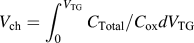 ${V_{{\rm{ch}}}} = \int_0^{{V_{{\rm{TG}}}}} {{C_{{\rm{Total}}}}/{C_{{\rm{ox}}}}d{V_{{\rm{TG}}}}}$
from the equivalent circuit. E
F is indeed the charging energy and is expressed as E
F
= eV
ch. As a result, C
Q can be estimated since C
Q is a function of E
F. Figure 5(c) shows C
ox, C
Q, and C
Total as a function of top gate voltage. C
Q increases as E
F increases for monolayer graphene, while
${V_{{\rm{ch}}}} = \int_0^{{V_{{\rm{TG}}}}} {{C_{{\rm{Total}}}}/{C_{{\rm{ox}}}}d{V_{{\rm{TG}}}}}$
from the equivalent circuit. E
F is indeed the charging energy and is expressed as E
F
= eV
ch. As a result, C
Q can be estimated since C
Q is a function of E
F. Figure 5(c) shows C
ox, C
Q, and C
Total as a function of top gate voltage. C
Q increases as E
F increases for monolayer graphene, while ${C_{{\rm{Si}}{{\rm{O}}_{\rm{2}}}}}$
is constant. As a result, C
Total depends on V
TG. For comparison,
${C_{{\rm{Si}}{{\rm{O}}_{\rm{2}}}}}$
is constant. As a result, C
Total depends on V
TG. For comparison, ${C_{{\rm{Si}}{{\rm{O}}_{\rm{2}}}}}$
(∼0.0383 μF/cm2) for the SiO2 thickness of 90 nm (this is a typical thickness for back gate SiO2) is also plotted, suggesting that the contribution of C
Q in C
Total can be neglected because of the small
${C_{{\rm{Si}}{{\rm{O}}_{\rm{2}}}}}$
(∼0.0383 μF/cm2) for the SiO2 thickness of 90 nm (this is a typical thickness for back gate SiO2) is also plotted, suggesting that the contribution of C
Q in C
Total can be neglected because of the small ${C_{{\rm{Si}}{{\rm{O}}_{\rm{2}}}}}$
value. Therefore, we do not generally discuss C
Q for back gate graphene devices. In other words, to extract C
Q, a top gate graphene device with a C
TG value comparable to the C
Q value is critical, which indicates the importance of the gate stack formation in Sec. II. On the other hand, from the device operation viewpoint, a large contribution of C
Q in C
Total means that inducing carriers in graphene is difficult. The inset in Fig. 5(c) shows the channel voltage (V
ch) calculated as a function of V
TG. V
ch is the voltage drop equivalent to the energy required to induce carriers in graphene. Thus, when V
TG = 1 V is applied, ∼30% of V
TG is spent in graphene itself and the actual voltage applied to the top gate insulator is reduced to be V = V
TG − V
ch. This is a common problem for high-mobility channels. However, consider C
Q positively as it can be the analytical tool used to extract DOS by the C−V measurement.
${C_{{\rm{Si}}{{\rm{O}}_{\rm{2}}}}}$
value. Therefore, we do not generally discuss C
Q for back gate graphene devices. In other words, to extract C
Q, a top gate graphene device with a C
TG value comparable to the C
Q value is critical, which indicates the importance of the gate stack formation in Sec. II. On the other hand, from the device operation viewpoint, a large contribution of C
Q in C
Total means that inducing carriers in graphene is difficult. The inset in Fig. 5(c) shows the channel voltage (V
ch) calculated as a function of V
TG. V
ch is the voltage drop equivalent to the energy required to induce carriers in graphene. Thus, when V
TG = 1 V is applied, ∼30% of V
TG is spent in graphene itself and the actual voltage applied to the top gate insulator is reduced to be V = V
TG − V
ch. This is a common problem for high-mobility channels. However, consider C
Q positively as it can be the analytical tool used to extract DOS by the C−V measurement.
(a) Schematic drawing of the graphene device and DOSs for metal and monolayer graphene. (b) Equivalent circuits with and without C
Q. (c) Capacitance as a function of V
TG. ${C_{{\rm{Si}}{{\rm{O}}_{\rm{2}}}}}$
for the SiO2 thickness of 4.5 nm, C
Q for monolayer graphene and their total capacitance (C
Total) are shown. For comparison,
${C_{{\rm{Si}}{{\rm{O}}_{\rm{2}}}}}$
for the SiO2 thickness of 4.5 nm, C
Q for monolayer graphene and their total capacitance (C
Total) are shown. For comparison, ${C_{{\rm{Si}}{{\rm{O}}_{\rm{2}}}}}$
for the SiO2 thickness of 90 nm is also indicated. Inset: Channel voltage [V
ch in (b)] as a function of V
TG.
${C_{{\rm{Si}}{{\rm{O}}_{\rm{2}}}}}$
for the SiO2 thickness of 90 nm is also indicated. Inset: Channel voltage [V
ch in (b)] as a function of V
TG.

Figure 6 shows the C
Q extracted from the C−V measurements for (a) monolayer graphene and (b) bilayer graphene, respectively.
Reference Kanayama, Nagashio, Nishimura and Toriumi25,Reference Kanayama and Nagashio26
It should be noted that the vertical axis on the right side is converted from C
Q to DOS using the relation of C
Q = e
2 DOS. The devices used in this analysis are the same as those in Fig. 3. For monolayer graphene, the estimated C
Q value is consistent with the theoretical dotted line values for E
F > ∼0.15 eV. The deviation from the theoretical value near the Dirac point is due to the residual carriers that are externally induced by the charged impurities.
Reference Ponomarenko, Yang, Gorbachev, Blake, Mayorov, Novoselov, Katsnelsonm and Geim14,Reference Nagashio, Nishimura and Toriumi40,Reference Adam, Hwang, Galitski and Das Sarma42
The residual carrier density (n*), as shown by the arrow in Fig. 6(a) is calculated as 3.6 × 1011 cm−2 using the relation of ${E_{\rm{F}}} = \hbar {v_{\rm{F}}}\sqrt {\pi {n^*}}$
, where ħ is the reduced Planck constant and v
F is the Fermi velocity. The n* values obtained from the C−V and I−V measurements are almost identical. Based on these results, it has been shown that graphene sandwiched between Y2O3 and SiO2 generally preserves the linear band structure with the exception being near the Dirac point. Although the electric band structure is generally determined experimentally by an angle-resolved photoemission spectroscopy (ARPES),
Reference Ohta, Bostwick, Seyller, Horn and Rotenberg43
the energy resolution in DOS obtained using the C
Q measurement is much higher than that by ARPES for the energy range of actual device operation.
${E_{\rm{F}}} = \hbar {v_{\rm{F}}}\sqrt {\pi {n^*}}$
, where ħ is the reduced Planck constant and v
F is the Fermi velocity. The n* values obtained from the C−V and I−V measurements are almost identical. Based on these results, it has been shown that graphene sandwiched between Y2O3 and SiO2 generally preserves the linear band structure with the exception being near the Dirac point. Although the electric band structure is generally determined experimentally by an angle-resolved photoemission spectroscopy (ARPES),
Reference Ohta, Bostwick, Seyller, Horn and Rotenberg43
the energy resolution in DOS obtained using the C
Q measurement is much higher than that by ARPES for the energy range of actual device operation.
(a) C Q as a function of E F for monolayer graphene. E F is evaluated as E F = eV ch. n* is the residual carrier density. Inset: The schematic drawing shows that the spatial distribution of charged impurities results in the variation of the Dirac point. (b) C Q as a function of E F for bilayer graphene. The E F formation is clearly observed as the external electrical field is increased.

On the other hand, the E
G formation (for bilayer graphene), where DOS becomes nearly zero, is clearly observed by increasing the displacement field $(\bar D)$
. The equation for
$(\bar D)$
. The equation for $\bar D$
is provided in the previous section. E
G is defined as the energy between inflection points for the conduction and valence sides in Fig. 6(b). E
G is roughly ∼0.3 V at
$\bar D$
is provided in the previous section. E
G is defined as the energy between inflection points for the conduction and valence sides in Fig. 6(b). E
G is roughly ∼0.3 V at $\bar D$
= 2.5 V/nm,
Reference Kanayama and Nagashio26
which corresponds to the maximum value expected from the theoretical calculation.
Reference McCann27
It should be emphasized that the DOS within the gap region almost reaches zero, which is not observed in the previous report for bilayer graphene with the h-BN top gate.
Reference Young, Dean, Meric, Sorgenfrei, Ren, Watanabe, Taniguchi, Hone, Shepard and Kim44
Moreover, the van Hove Singularity is also observed near the valence band edge, as shown by arrows. In the case of the I−V measurement, the temperature dependence of the resistivity at the Dirac point must be measured to determine E
G. However, E
G can be determined directly from the C
Q measurement because the scattering factor is not included in the C−V measurement.
$\bar D$
= 2.5 V/nm,
Reference Kanayama and Nagashio26
which corresponds to the maximum value expected from the theoretical calculation.
Reference McCann27
It should be emphasized that the DOS within the gap region almost reaches zero, which is not observed in the previous report for bilayer graphene with the h-BN top gate.
Reference Young, Dean, Meric, Sorgenfrei, Ren, Watanabe, Taniguchi, Hone, Shepard and Kim44
Moreover, the van Hove Singularity is also observed near the valence band edge, as shown by arrows. In the case of the I−V measurement, the temperature dependence of the resistivity at the Dirac point must be measured to determine E
G. However, E
G can be determined directly from the C
Q measurement because the scattering factor is not included in the C−V measurement.
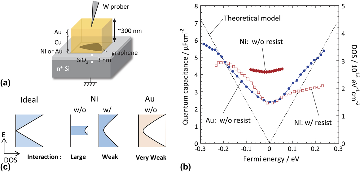
Finally, the application of the C Q measurement to the metal/graphene contact in the graphene FET is described. Reference Ifuku, Nagashio, Nishimura and Toriumi45 In terms of electron device miniaturization, the electrical contacts are critically important to reduce the total resistance. Reference Nagashio and Toriumi46 This is more significant in the higher carrier mobility channel. Although no Schottky barrier exists at the graphene/metal interface due to the lack of a band gap, the contact resistivity is intrinsically high due to the small DOS in graphene. Reference Nagashio and Toriumi46 It is known that the DOS of monolayer graphene increases with contact to the metal due to the orbital hybridization, that is, π − d coupling. Reference Hammer and Norskov47 The typical chemisorption group is Ni, while the typical physisorption group is Au. Reference Giovannetti, Khomyakov, Brocks, Karpan, van der Brink and Kelly48 Here, our strategy is the reduction of the contact resistivity by the π − d coupling with Ni. For this purpose, the DOS of graphene in contact with the metals should be estimated through the C Q measurement. Figure 7(a) shows the schematic drawing of the experimental setup. The thickness of the back gate SiO2 in the metal/graphene/SiO2/n +-Si contact structure is reduced to ∼3 nm to extract the C Q. Even for ∼3 nm thickness of SiO2, monolayer graphene can be identified by the optical contrast under the optical microscope, which is supported by our calculation on the visibility of graphene on SiO2. The key technique used here is the resist-free metal deposition process using the finely patterned PMMA shadow masks, which enables us to extract the “intrinsic” metal/graphene interaction. Many researchers have reported that the resist residue remains on graphene. Reference Ishigami, Chen, Cullen, Fuhrer and Willians49–Reference Goossens, Calado, Barreiro, Watanabe, Taniguchi and Vandersypen51 The resist residue is a serious concern in light of the fact that activated carbon, whose hydrophobic surface attracts organic materials, is composed of graphene. Reference Acharya, Strano, Mathews, Billinge, Petkov, Subramoney and Foley52 Fig. 7(b) shows the DOS extracted from the C Q measurements. For the resist-free metal/graphene contacts, graphene underneath the Au electrode maintains the linear DOS—energy relation except near the Dirac point, while the DOS of graphene underneath the Ni electrode is broken and largely enhanced around the Dirac point, resulting in only a slight modulation of the Fermi energy in the graphene. On the other hand, when Ni is deposited using the polymer resist, the traces of linear dispersion of the graphene can be observed, which is also seen in the I−V curve. Reference Bartolomeo, Giubileo, Romeo, Sabatino, Carapella, Iemmo, Schroeder and Lupina53 Fig. 7(c) summaries the DOS—energy relation for monolayer graphene modified with the metal contact. The contact resistivity measurements using the resist-free metal deposition technique show that the contact resistivity obtained for the Ni electrode has been reduced to ∼1500 Ω μm because of the increase in the DOS by the π − d coupling. Reference Ifuku, Nagashio, Nishimura and Toriumi45 Although this contact resistivity value is still high for the requirement, the present experiment clearly suggest that one of effective guidelines to reduce the contact resistivity is the increase in the DOS of graphene underneath the metal electrode.
(a) Schematic of the metal/graphene/SiO2/n
+-Si device to extract C
Q for metal/graphene structure. The thickness of SiO2 is reduced to 3 nm, which results in a ${C_{{\rm{Si}}{{\rm{O}}_{\rm{2}}}}}$
comparable to C
Q. (b) The experimentally extracted C
Q of graphene in contact with metals. Solid red circle, open red rectangular, and solid blue circle represent the resist-processed Ni, resist-free Ni, and resist-free Au devices, respectively. (c) Summary of DOS—energy relation after the metal/graphene interaction suggested from the C
Q measurements.
${C_{{\rm{Si}}{{\rm{O}}_{\rm{2}}}}}$
comparable to C
Q. (b) The experimentally extracted C
Q of graphene in contact with metals. Solid red circle, open red rectangular, and solid blue circle represent the resist-processed Ni, resist-free Ni, and resist-free Au devices, respectively. (c) Summary of DOS—energy relation after the metal/graphene interaction suggested from the C
Q measurements.
IV. CONCLUSIONS
In this paper, we have discussed the gate stack formation in graphene FETs and the extraction of DOS through C Q measurements. The top gate formation, which appears at first glance to be quite easy, is actually very difficult because defects are easily introduced in graphene by the conventional deposition techniques for high-k oxides. The improvement of the gate stack process in graphene research enables the extraction of DOS through the C Q measurement. It is shown that the electric band structure of graphene in contact with gate insulators or metal electrode deviates from the intrinsic band gap structure. Through the extension of this technique, a further understanding of the graphene/insulator and the graphene/metal interfaces is needed to fabricate graphene FETs.
ACKNOWLEDGMENTS
We are grateful to Covalent Materials for kindly providing the Kish graphite and to Drs T. Taniguchi and K. Watanabe of the National Institute of Materials Science (NIMS) for kindly providing the h-BN crystals. This research was partly supported by JSPS KAKENHI Grant Numbers JP25107004, JP16H04343, and JP16K14446.


 Open access

