




I. INTRODUCTION
Organic photovoltaic (OPV) devices offer the potential for low-cost and large-area solar cells. Reference Krebs1 Ultrathin and flexible OPV devices also enable building and transport integration in products such as windows, transparent roofs, or car windshields. Reference Brabec, Gowrisanker, Halls, Laird, Jia and Williams2,Reference Guo, Ameri, Forberich and Brabec3 OPVs are particularly attractive because of the ability to manufacture them using high throughput printing processes. Reference Krebs, Jørgensen, Norrman, Hagemann, Alstrup, Nielsen, Fyenbo, Larsen and Kristensen4 A popular choice for the active layer of OPVs is the bulk heterojunction (BHJ) formed by blending together electron-donating and electron-accepting species (either polymers or small molecules). A long-established and well-studied choice for such a blend consists of a fullerene derivative and a conjugated polymer. Reference Liu, Gu, Jung, Jo and Russell5,Reference Dang, Hirsch and Wantz6 Here, the BHJ consists of a complex morphology that is designed to enable efficient separation of charges at the interface between the electron-donating polymer and the electron-accepting fullerene. Reference Günes, Neugebauer and Sariciftci7 The requirement for large interfacial area needs to be balanced by the provision of a continuous path for electron and hole transport. Reference Günes, Neugebauer and Sariciftci7 A full characterization and understanding of the morphology formed during device fabrication, and the potential evolution of structure/morphology during operation, Reference Li, Ho Chiu, Shahid Ashraf, Fearn, Dattani, Cheng Wong, Tan, Wu, Cabral and Durrant8 is challenging because a number of different processes, such as phase separation, surface or substrate enrichment Reference Parnell, Dunbar, Pearson, Staniec, Dennison, Hamamatsu, Skoda, Lidzey and Jones9 and crystallization (potentially of both components), Reference Brabec, Gowrisanker, Halls, Laird, Jia and Williams2,Reference Dang, Hirsch and Wantz6 may contribute to the final film structure and device performance. It is hoped that the development of further understanding of the morphology of OPV materials in thin-film architectures will underpin the successful commercial application of OPVs. Reference Brabec, Gowrisanker, Halls, Laird, Jia and Williams2,Reference Liu, Gu, Jung, Jo and Russell5,Reference Dennler, Scharber and Brabec10,Reference Lee, Schwenn, Smith, Cavaye, Shaw, James, Krueger, Gentle, Meredith and Burn11 This paper describes a study that focusses on conjugated polymer/fullerene mixing, by looking at the evolution of morphology within a simplified (bilayer) geometry, as a function of the polymer film thickness and temperature.
To understand the process controlling the morphology of fullerene and polymer OPVs, several studies on bilayers constructed from [6,6]-phenyl C61-butyric acid methyl ester (PCBM) and poly(3-hexylthiophene) (P3HT) have been carried out. Reference Lee, Schwenn, Smith, Cavaye, Shaw, James, Krueger, Gentle, Meredith and Burn11–Reference Chen, Liu, Wang, Nakahara and Russell20 These bilayers initially consisted of pure P3HT and PCBM layers, with thermal annealing used as a means to study the intermixing of the PCBM and P3HT. A number of studies have shown that PCBM and P3HT can rapidly intermix, Reference Lee, Schwenn, Smith, Cavaye, Shaw, James, Krueger, Gentle, Meredith and Burn11,Reference Treat, Brady, Smith, Toney, Kramer, Hawker and Chabinyc14,Reference Tada, Geng, Wei, Hashimoto and Tajima18,Reference Gevaerts, Koster, Wienk and Janssen19 and that this mixing involves diffusion of PCBM into amorphous regions of the P3HT. However, in PCBM/regioregular-P3HT bilayers, there are significant quantitative differences between the composition profiles in some of these studies. Treat et al. observed a uniform distribution of PCBM across 450 nm bilayers after 5 min of annealing at 150 °C, Reference Treat, Brady, Smith, Toney, Kramer, Hawker and Chabinyc14 indicative of a PCBM loading of 40%. In contrast, D. Chen et al., working in thinner bilayers but at similar annealing times and temperatures, observed only partial mixing, even though the PCBM constituted less than 40% of the total amount of material in the film. Reference Chen, Liu, Wang, Nakahara and Russell20 Both of these studies used dynamic secondary ion mass spectroscopy (DSIMS). Neutron reflectivity allows depth profiles to be determined with significantly higher resolution, and also allows for time-dependent (in situ) measurements. Reference Clulow, Armin, Lee, Pandey, Tao, Velusamy, James, Nelson, Burn, Gentle and Meredith21,Reference Higgins, Sferrazza, Jones, Jukes, Sharp, Dryden and Webster22 In addition to the measurement of layer composition offered by ion beam methods and ellipsometry, Reference Leman, Kelly, Ness, Engmann, Herzing, Snyder, Ro, Kline, DeLongchamp and Richter23,Reference Ferenczi, Nelson, Belton, Ballantyne, Campoy-Quiles, Braun and Bradley24 this increased resolution allows characterization of roughness at buried polymer interfaces, which is typically on the order of a few nanometers. Reference Jones and Richards25 Neutron reflectivity was performed on several P3HT/PCBM bilayers with different ratios of PCBM to P3HT by H. Chen et al. Reference Chen, Hegde, Browning and Dadmun17 They reported only partial mixing in bilayers after annealing for 60 min at 150 °C, a maximum loading of ∼22% PCBM in the P3HT-rich layer, and surface enrichment of PCBM within the P3HT-rich (top) layer.
In this paper we look at the mixing between PCBM and regioregular P3HT as a function of film thickness and annealing temperature. We adopt the robust methodology that we have used in our previous studies of PCBM/polymer bilayers Reference Môn, Higgins, James, Hampton, Macdonald, Ward, Gutfreund, Lilliu and Rawle26 and use a combination of in situ annealing (annealing a sample in the neutron beam) and ex situ annealing (annealing a sample before measuring the reflectivity). Our results add to the strong body of evidence that there is rapid intermixing between PCBM and P3HT, and support the work of H. Chen et al. Reference Chen, Hegde, Browning and Dadmun17 —giving a maximum loading of PCBM in P3HT of around 20%. However, we find contrasting (and rather subtle) results in comparison with the reported findings of H. Chen et al., in relation to PCBM-enrichment at the free surface.
II. EXPERIMENTAL PROCEDURES
A. Materials
PCBM, with 99.5% purity, was obtained from Solenne BV (Groningen, The Netherlands). P3HT (weight-average molecular weight 36,000, polydispersity index 1.8, regioregularity 91–94%) was supplied by Rieke Metals (Lincoln, Nebraska). Silicon [(100) with native oxide layer] was obtained from Prolog Semicor (Kiev, Ukraine). Mica sheets were obtained from Goodfellow (Huntingdon, United Kingdom). Toluene and chlorobenzene were purchased from Sigma-Aldrich (St. Louis, Missouri).
B. Sample fabrication
P3HT layers were spin-coated onto freshly-cleaved mica from toluene solutions (0.1, 1, and 2 wt% for the 8 nm, 35 nm, and 80 nm films respectively). PCBM layers were spin-coated from a chlorobenzene solution (1 wt%) onto 2-inch diameter silicon substrates. A spin speed of 1000 revolutions per minute was used for all films. The spin-coated mica/P3HT layers and substrate/PCBM layers were then left for 24 h under vacuum before bilayer fabrication. Silicon/PCBM/P3HT bilayers were prepared by floating the P3HT layer onto the surface of de-ionized water, and then depositing this layer onto the silicon/PCBM sample. Newly fabricated bilayers were firstly allowed to dry at ambient conditions and were then left under vacuum for 24 h, before annealing.
C. In situ annealing
Samples were annealed on the neutron reflectivity beam-line, in a nitrogen atmosphere. The sample surface temperature during in situ annealing was calibrated by attaching an external thermocouple to the surface of duplicate silicon samples. There is a slight temperature overshoot (of a few °C) at the start of in situ annealing, and the quoted temperature of 170 °C, represents the approximate maximum sample surface temperatures reached during annealing. To keep this overshoot to a minimum the temperature was increased in two steps; an intermediate step from room temperature to 80 °C, followed by a step from 80 to 170 °C. A full reflectivity curve was measured at 80 °C (this took 90 min) and the temperature was then raised to 170 °C.
D. Ex situ annealing
Neutron reflectivity samples were annealed in the dark in a vacuum oven (Binder Inc., Bohemia, New York) with a vacuum of ∼10−3 Torr. Sample surface temperatures were calibrated by attaching an external thermocouple to the surface of duplicate silicon samples in the oven. At the end of annealing, samples were removed from the oven and rapidly quenched to room temperature on a metal surface. All quoted temperatures for ex situ annealed samples refer to the sample surface temperature. In contrast to the in situ annealing, there was no intermediate step here. The samples were heated to the annealing temperature in one go.
E. Atomic force microscopy (AFM)
Tapping mode was used on a Dimension-3100 (Veeco, New York, New York) or a CE100 (Park Systems Corporation, Suwon, South Korea), with OTESPA (Bruker Corporation, Billerica, Massachusetts) cantilevers to measure sample surface morphology and to determine initial bilayer film thicknesses. Film thickness was determined by scratching the surface of a single layer on a silicon substrate and scanning across the step edge of the scratch.
F. Neutron reflectivity
Measurements were carried out using beam-line D17 at the Institut Laue-Langevin (ILL) in time-of-flight (TOF) mode. Reference Cubitt and Fragneto27 TOF uses a broad range of neutron wavelengths at a fixed incident angle. At D17 two incident angles were used to cover the full reflectivity range, down to a reflectivity of approximately 10−6. Specular reflectivity was extracted using the program COSMOS within the Large Array Manipulation Program (LAMP) distributed by the ILL. Two incident-angles (0.6 and 2.4°) were used to produce a full reflectivity curve, with resolution ranging from 2.3% at low momentum-transfer (q), to 4.9% at high q. Measurements during in situ annealing used a single angle of 1°, but with chopper settings that gave a higher flux of neutrons. This angle just captured the critical edge for the sample, gave a lower q range and a lower resolution (between 4.1 and 8.1%), but the higher flux allowed much shorter acquisition-times. Samples were exposed to the neutron beam for acquisition-times of 30 min at 0.6°, 60 min at 2.4° and in 30 s time-slices at 1°.
Reflectivity was fitted using Parratt32 and Motofit. 28 Each layer was characterized by a thickness and scattering length density (SLD), plus an interfacial roughness between adjacent layers (σ). The instrumental resolution was included within the models for all samples, at the values calculated from the slit widths and chopper settings. Except where stated otherwise, samples were fitted using fixed silicon and native silicon oxide layer parameters. The silicon substrate SLD was fixed at 2.07 × 10⁻⁶ Å−2. The silicon substrate σ was fixed at 0.7 nm. The native silicon oxide layer parameters were fixed at the following values; SLD = 3.48 × 10⁻⁶ Å−2, thickness = 1.5 nm, and σ = 0.7 nm.
SLDs for pure P3HT and PCBM were first calculated using the National Institute of Standards and Technology (NIST) SLD calculator 29 with literature density values. Reference Treat, Brady, Smith, Toney, Kramer, Hawker and Chabinyc14,Reference Chen, Hegde, Browning and Dadmun17,Reference Lee and Dadmun30 The calculated value for PCBM was 4.4 × 10⁻⁶ Å−2 and for P3HT was 0.62 × 10⁻⁶ Å−2. These values were used as initial guesses when fitting the reflectivity curves of unannealed bilayers and ex situ annealed bilayers. For the in situ sample, the fit parameters from the previous time slot in the kinetic series were used as the initial guesses.
The percentage (by volume) of PCBM in the each layer was calculated using:
 $$100 \times {{\left( {{\rm{SL}}{{\rm{D}}^{{\rm{layer}}}} - {\rm{SL}}{{\rm{D}}^{{\rm{pure}}\,{\rm{P3HT}}}}} \right)} \over {\left( {{\rm{SL}}{{\rm{D}}^{{\rm{pure}}\,{\rm{PCBM}}}} - {\rm{SL}}{{\rm{D}}^{{\rm{pure}}\,{\rm{P3HT}}}}} \right)}}\quad ,$$
where SLD i is the SLD of layer i, and the SLDs of pure P3HT and pure PCBM were set to the above calculated values.
G. Optical microscopy
Images were obtained using a Nikon Eclipse-E600FN microscope (Nikon, Tokyo, Japan), using a 50× objective.
III. RESULTS AND DISCUSSION
The reflectivity data from a bilayer measured at 80 °C and the corresponding fit obtained using a two-layer model are shown in Fig. 1(a). Figure 1(b) shows the fitted SLD profile. The SLD of the PCBM layer is 4.30 × 10⁻⁶ Å−2, and the SLD of the P3HT layer is 0.62 × 10⁻⁶ Å−2. These values correspond reasonably closely to previously reported values. Reference Chen, Hegde, Browning and Dadmun17,Reference Ro, Akgun, Connor, Hammond, Kline, Snyder, Satija, Ayzner, Toney, Soles and Delongchamp31 The interfacial roughness, σ, between the two layers is 1.2 nm. This SLD profile corresponds closely to that of an as-fabricated PCBM/polymer bilayer (see e.g., Môn et al. Reference Môn, Higgins, James, Hampton, Macdonald, Ward, Gutfreund, Lilliu and Rawle26 ), and shows that little (if any) interdiffusion has occurred during the temperature step from room temperature to 80 °C. We note that the data shown in Fig. 1 clearly has significantly more pronounced fringes in the reflectivity and a sharper interface than the unannealed PCBM/P3HT bilayer (with a 15 nm PCBM layer) fabricated by H. Chen et al. (Figs. 1 and 2). Reference Chen, Hegde, Browning and Dadmun17
(a) Reflectivity versus momentum transfer normal to the substrate (q), and fit for an unannealed PCBM (∼20 nm)/P3HT (∼35 nm) bilayer on silicon. (b) The SLD profile corresponding to the best-fit line in (a). Fits were obtained using a bilayer model in which the thickness, SLD and roughness of each layer was allowed to vary.

Temperature versus in situ annealing time, for a nominal temperature of 170 °C. The dashed line shows the set-point temperature and the continuous line shows the sample surface temperature.

The sample from Fig. 1 was then annealed in situ for 30 min. In situ annealing allows the reflectivity to be modeled from a known starting composition-profile, from which the subsequent SLD profile evolution can be followed in small steps. The sample temperature measurement in Fig. 2 shows that there was an initial period of approximately 5 min, during which the sample temperature increased from 80 to approximately 170 °C, followed by a 10 min period of temperature stabilization and a 15 min period of annealing at a constant temperature. The sample was then allowed to cool. Once the sample had again reached 80 °C, another full reflectivity curve was measured.
The reflectivity data, fits and SLD profiles for the sample are shown in Fig. 3. The data is well-fitted using a simple bilayer model (i.e., two layers of uniform composition, separated by an interface parameterized by Gaussian roughness Reference Jones and Richards25,Reference Higgins and Benoit32,Reference Roe33 ) at all stages of annealing. Figure 3(a) shows how the reflectivity from this 35 nm P3HT bilayer sample changed with annealing. There is a clear change in the periodicity of the Kiessig fringes, indicative of significant changes in the composition profile within the sample. Figure 3(b) shows the SLD profile normal to the substrate for various annealing times and Fig. 4 shows the evolution of some of the fit parameters during annealing. In comparison to the composition profile at 80 °C, the SLD profile progressed in three clear ways during annealing at 170 °C; (i) the bottom layer SLD reduced; (ii) the top layer SLD increased; (iii) the interface roughness between the top and bottom layers increased. Small changes may be attributed to thermal expansion/contraction during heating/cooling (see Leman et al. Supplementary Material Reference Leman, Kelly, Ness, Engmann, Herzing, Snyder, Ro, Kline, DeLongchamp and Richter23 ). However, this would only account for approximately a 1.5% change in SLD between 80 and 170 °C. Systematic changes in the composition profile are complete within 15 min, or possibly earlier. The ability to discriminate more precise kinetics in the time period before 15 min is confounded by scatter in the fit parameters, potential correlations between fit parameters (given the restricted q-range, lower resolution, and poorer statistics of the 30 s time-slices in comparison to the full reflectivity curves), and sample surface temperature stabilization. Scatter in the fit parameters is most evident for the top layer SLD. This is likely to be a result of the fact that the SLD of this layer is much lower than the bottom layer, resulting in the SLD of this layer having less of a constraining influence on the model reflectivity than that of the bottom layer (variation in the SLD-contrast at the interface, of a given magnitude, is a much larger fraction of the SLD of the top layer in comparison to the bottom layer). Figures 3 and 4 also show the changes in the composition profile obtained from fits of the full reflectivity curves before and after annealing. This data shows a difference in the fitted bottom layer SLD after annealing (∼3.7 × 10⁻⁶ Å−2) in comparison to the fit during annealing (∼3.2 × 10⁻⁶ Å−2). Given the differences between the quality of the measurements during and before/after annealing discussed above it is entirely possible, indeed likely, that this apparent change is a measurement artifact. However, in comparison with the SLD profile before annealing, the SLD profile after-annealing confirms the overall trend in the layer SLDs and interfacial roughness found during annealing. The composition profile after annealing has bottom and top layers of 81% PCBM and 19% PCBM respectively, and an interface roughness of 5.1 nm.
(a) Neutron reflectivity data and (b) SLD profiles from a PCBM (∼20 nm)/P3HT (∼35 nm) bilayer annealed in situ at 170 °C. Reflectivity curves are offset vertically for clarity. The lines in (a) are bilayer fits to the experimental data. The percentage PCBM in each layer and interface roughness, σ, are shown for the SLD profile after annealing. The measurements before-annealing and after-annealing were performed at 80 °C. The times given in the legend are those at the end of each 30 s time slice.

Fit parameters for the PCBM (∼20 nm)/P3HT (∼35 nm) sample annealed in situ at 170 °C. The reflectivity curves and SLD profiles for this sample are shown in Fig. 3. The filled circles correspond to fits of the full reflectivity curves before and after annealing the sample. The open squares correspond to fits of the reflectivity collected at a single incident angle during annealing (30 s collection time for each data point). The SLD of the bottom and top layers are shown in (a) and (b) respectively, and the interface roughness between these two layers is shown in (c).

The changes observed indicate that there has been a significant transfer of PCBM into the initially pure P3HT layer producing a P3HT-rich layer, and a transfer of P3HT into the initially pure PCBM layer producing a PCBM-rich layer, in a time frame of less than a few minutes. This is consistent with previous results in similar PCBM/P3HT bilayers. Reference Treat, Brady, Smith, Toney, Kramer, Hawker and Chabinyc14,Reference Chen, Hegde, Browning and Dadmun17 The migration of both species in this system can be contrasted with our findings for PCBM/polystyrene (PS) bilayers, using the same thickness PCBM (the same batch of material, spin-coated from the same solvent). Reference Môn, Higgins, James, Hampton, Macdonald, Ward, Gutfreund, Lilliu and Rawle26 In the simpler PCBM/PS system (in which only the PCBM can crystallize) mixing also occurred very rapidly, but here only the PCBM diffuses into the PS, with no PS migrating into the PCBM. The PCBM/PS system forms a consistent composition profile (between a PS-rich phase and a pure PCBM phase) that is suggestive of an equilibrium liquid–liquid interface (on the basis that the interface forms before any PCBM crystallizes, and is independent of annealing temperature and film thickness). The situation is very different for regioregular P3HT/PCBM, as the as-cast polymer film contains extensive crystalline regions (see Supplementary Material Fig. S1 and previous studies Reference Ro, Akgun, Connor, Hammond, Kline, Snyder, Satija, Ayzner, Toney, Soles and Delongchamp31,Reference Verploegen, Mondal, Bettinger, Sok, Toney and Bao34,Reference Hopkinson, Staniec, Pearson, Dunbar, Wang, Ryan, Jones, Lidzey and Donald35 ).
In our previous investigations of annealed PCBM (20 nm)/PS bilayers, we found a very strong influence of the polymer film thickness and temperature on the crystallization behavior of the PCBM, but no influence on the composition profile within the bilayer. Reference Môn, Higgins, James, Hampton, Macdonald, Ward, Gutfreund, Lilliu and Rawle26 To see how film thickness and temperature affect the mixing in the PCBM/P3HT system, bilayers with 20 nm of PCBM on the bottom and P3HT layers of various thicknesses on top, were annealed at 140 °C. Figure 5 shows the reflectivity data and SLD profiles obtained from bilayer/single layer fits with three different P3HT thicknesses, after ex situ annealing. As with the in situ measurements, migration of PCBM into the P3HT layer on annealing is evident for all three thicknesses of P3HT. A simple bilayer model fits the 8 and 35 nm P3HT sample data well [Figs. 5(a) and 5(b)]. For the 8 nm P3HT sample the best-fit has a PCBM-rich layer containing 90–98% PCBM and a P3HT-rich layer containing ∼7–19% PCBM. For the 35 nm P3HT sample the best-fit PCBM-rich layer contains 84–85% PCBM and the P3HT-rich layer contains 18–20% PCBM. The roughness of the buried PCBM-rich/P3HT-rich interface has best-fit values of 2.4–2.7 nm and 3.3–3.8 nm for the 8 nm P3HT and 35 nm P3HT samples respectively. The composition and interfacial roughness ranges quoted here refer to best fits which were obtained by independent repeats of the data reduction and fitting methodology. The robustness of the fit parameters with-respect-to the inclusion/neglect of the oxide layer was also tested, and found to be negligible. It is important to point out that the PCBM concentration in the P3HT-rich (top) layer in the 8 nm P3HT sample is subject to significantly more uncertainty than the other layer concentrations in the fits of both the 8 and 35 nm P3HT samples, due to the fact that this sample consists of a very thin layer of low SLD material on top of a thicker layer of higher SLD. However, it is clear that significant mixing has occurred in this sample, as the data cannot be fitted well using pure P3HT and PCBM layer SLDs. A final test of the robustness of our modeling is provided by using an alternative approach to fit the data. Rather than using a bilayer model, with the gradient in SLD at the buried interface described by Gaussian roughness, a much larger number of discrete thin layers with adjustable SLD, but zero roughness between the layers is used to describe the SLD profile. The 20-layer fit in Fig. 5(e) shows a very similar SLD profile to the bilayer fit.
Neutron reflectivity data and fits for PCBM (20 nm)/P3HT bilayers on silicon, with three different thicknesses of P3HT. (a–c) Neutron reflectivity data and fits. All fits use either a single layer or bilayer model in which the thickness, SLD and roughness of each layer is allowed to vary. The SLD profiles corresponding to the best-fit lines in (a–c) are given in (d–f) respectively. Initial thicknesses of P3HT were approximately 8 nm in (a) and (d), 35 nm in (b) and (e) and 80 nm in (c) and (f). All samples were ex situ annealed at 140 °C (for 60 min for the 8 and 35 nm P3HT bilayers, and for 10 min for the 80 nm P3HT bilayer). A 20 layer fit to the 35 nm P3HT sample is also shown in (e); in this fit the interfacial roughness between all layers is set to zero, and the SLD of all layers is allowed to vary. There is no fixed oxide layer included in this model. There is also no fixed oxide layer included in the single/bilayer fits in (c) and (f). The unannealed SLD profiles in (d), (e) and (f) were calculated from AFM measurements (of the layer thicknesses and the surface roughness) of duplicate PCBM and P3HT single layers, and of the bilayer samples prior to annealing (imaging peripheral areas of the sample that were not irradiated by the neutron beam). The percentages (by volume) of PCBM in each layer and the roughness of the PCBM-rich/P3HT-rich interface, after annealing are given in (e) for the 2 layer fit to this sample. The inset in (c) shows the same data/fits presented in ‘ $R_{\rm{q}}^4$
’ format.
$R_{\rm{q}}^4$
’ format.

Our results show a close similarity between the reflectivity curves and fitted SLD profiles for 20 nm PCBM/35 nm P3HT bilayers after annealing at both 170 °C [Figs. 3(a) and 3(b)] and 140 °C [Figs. 5(b) and 5(e)]. We now discuss this with regard to the state (crystalline/amorphous) of the PCBM and P3HT within the bilayers. Grazing-incidence X-ray diffraction (GIXD) measurements (see Supplementary Material Fig. S1) show extensive P3HT crystallization, but little evidence of significant PCBM crystallization on annealing at 140 °C. GIXD measurements were not performed in parallel with the in situ neutron reflectivity measurements at 170 °C. However, it is quite likely that some PCBM nanocrystallisation occurs at 170 °C, if not on the timescale of the rapid mixing shown in Fig. 3, then within the 30 min annealing time (Leman et al. Reference Leman, Kelly, Ness, Engmann, Herzing, Snyder, Ro, Kline, DeLongchamp and Richter23 report crystallization of PCBM within a similar PCBM/P3HT bilayer, but with the PCBM layer on top, annealed at 160 °C for 10 min). Given the strong temperature dependence of the crystallization of PCBM between 140 and 170 °C, Reference Verploegen, Mondal, Bettinger, Sok, Toney and Bao34 and the high levels of crystalline material in spin-coated P3HT, Reference Ro, Akgun, Connor, Hammond, Kline, Snyder, Satija, Ayzner, Toney, Soles and Delongchamp31,Reference Verploegen, Mondal, Bettinger, Sok, Toney and Bao34,Reference Hopkinson, Staniec, Pearson, Dunbar, Wang, Ryan, Jones, Lidzey and Donald35 the similar SLD profiles are what one would expect in a system where there is rapid diffusion of PCBM into the amorphous P3HT regions, with little change in the fraction of amorphous P3HT and little influence of any PCBM crystallization that may occur at 170 °C, during this rapid diffusion process. A similar lack of sensitivity to annealing temperature is found for PCBM/PS bilayers, but for a completely different reason. Migration of PCBM into PS also occurs within a few minutes and gives similar SLD profiles at both 140 and 170 °C. Reference Môn, Higgins, James, Hampton, Macdonald, Ward, Gutfreund, Lilliu and Rawle26 However, in the case of PCBM/PS the composition profile is established in the absence of any crystallization, whereas in P3HT/PCBM the composition profile is likely to be largely determined by the volume fraction and micro/nano-structure of the pre-existing crystalline/amorphous regions within the polymer layer prior to bilayer annealing. Reference Ro, Akgun, Connor, Hammond, Kline, Snyder, Satija, Ayzner, Toney, Soles and Delongchamp31
For the 80 nm P3HT sample, the reflectivity curve is modeled reasonably well using a single layer fit (in which the SLD, thickness and roughness of the layer are allowed to vary), indicating that there is ‘almost’ complete mixing of PCBM and amorphous P3HT [see Figs. 5(c) and 5(f)]. However, this fit has an integrated SLD that is much too high (by a factor of ∼40%; see Table SI in the Supplementary Material), given the known composition of the sample. Figure 5(f) also shows a bilayer fit for the 80 nm P3HT sample (in which the SLDs, thicknesses, and roughnesses of both layers are allowed to vary). This fit is visually better and has a lower value of the goodness-of-fit reduced chi-squared parameter, $\chi _\nu ^2$
,
Reference Hughes and Hase36
compared to the single layer fit, but still has an integrated SLD that is unphysically high. Further approaches to fit the reflectivity from this sample were made using a number of different multilayer models. These approaches highlight the potential for nonuniqueness, in terms of different models that can adequately fit the data for the 80 nm P3HT sample, and hence place limits on the precision with which it is possible to describe the details of the composition profile in this sample. Discussion of these different approaches and the degree to which we are able to determine details of the composition profile is provided in the supplementary material (see Fig. S2 and accompanying discussion). The main conclusion from this discussion is that, despite the existence of significant uncertainty over the exact distribution of PCBM within the 80 nm P3HT sample, the physical picture represented by the reflectivity curve in Fig. 5(c) corresponds to a situation in which the entire PCBM bottom layer has mixed into the P3HT layer on top.
$\chi _\nu ^2$
,
Reference Hughes and Hase36
compared to the single layer fit, but still has an integrated SLD that is unphysically high. Further approaches to fit the reflectivity from this sample were made using a number of different multilayer models. These approaches highlight the potential for nonuniqueness, in terms of different models that can adequately fit the data for the 80 nm P3HT sample, and hence place limits on the precision with which it is possible to describe the details of the composition profile in this sample. Discussion of these different approaches and the degree to which we are able to determine details of the composition profile is provided in the supplementary material (see Fig. S2 and accompanying discussion). The main conclusion from this discussion is that, despite the existence of significant uncertainty over the exact distribution of PCBM within the 80 nm P3HT sample, the physical picture represented by the reflectivity curve in Fig. 5(c) corresponds to a situation in which the entire PCBM bottom layer has mixed into the P3HT layer on top.
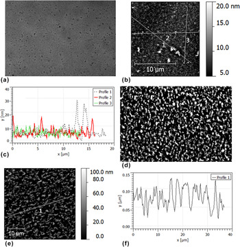
We also assessed the morphology of annealed bilayers using optical microscopy and AFM. This involved the samples used for the neutron reflectivity measurements and duplicate samples, annealed for various times at different temperatures. Fig. S3 shows the emergence of micron-sized PCBM crystals previously reported in bilayers annealed for 120 min. Reference Môn, Higgins, James, Hampton, Macdonald, Ward, Gutfreund, Lilliu and Rawle26 No emergence of such crystals was seen in the samples used for neutron reflectivity (annealed for 60 min or less). Figure 6 shows typical surface morphology on the 35 and 80 nm P3HT neutron reflectivity samples annealed at 140 °C. The morphology of the 35 nm P3HT sample consists of discrete features of around 10–25 nm in height separated by several microns or more. There is no sign of any dewetting on this sample (in contrast to the report by Ro et al. Reference Ro, Akgun, Connor, Hammond, Kline, Snyder, Satija, Ayzner, Toney, Soles and Delongchamp31 for P3HT/PCBM bilayers with the PCBM layer on top), and the root-mean-square (rms) roughness of the surface is small compared to the total bilayer thickness or the thickness of the P3HT layer (the maximum peak-to-trough height seen in profile 1 of Fig. 6(c) is also lower than the P3HT layer thickness). This negates the possibility that the reduction in the SLD of the bottom layer in Fig. 5(e) is due to lateral averaging of the SLD profile (averaged over the in-plane coherence length of the neutrons - tens of microns Reference Richardson, Webster and Zarbakhsh37,Reference Russell38 ) over regions that contain significant macroscopic (micron-sized) surface holes that penetrate into the bottom 20 nm of the sample. This is also the case for the 35 nm P3HT bilayer annealed in situ at 170 °C; In comparison to the 35 nm P3HT sample, ex situ annealed at 140 °C, this sample shows different ‘dot-like’ morphological features on the sample surface (see Fig. S4). We do not understand the reason for this morphological difference at present.
Optical microscopy and atomic force microscopy (AFM) images of annealed (20 nm) PCBM/P3HT bilayers. (a) Optical microscopy image of a 35 nm P3HT bilayer annealed at 140 °C for 60 min. (b) AFM image of the sample shown in (a). (c) Line profiles from the image shown in (b). (d) Optical microscopy of an 80 nm P3HT bilayer annealed at 140 °C for 10 min. (e) AFM image of an 80 nm P3HT bilayer annealed at 140 °C for 60 min. (f) A line profile from the image shown in (e). (a–d) were taken from the actual samples measured with neutron reflectivity, while (e) and (f) are from a duplicate of the sample show in (d), but annealed for 60 min, rather than the 10 min (both AFM measurements and optical microscopy images on these two samples look very similar). The rms roughnesses of (b) and (e) are 2.7 and 26 nm respectively. AFM measurements (not shown) on the sample shown in (d) gave an rms roughness of 24 ± 2 nm (averaged over five 40 × 40 μm scans from different parts of the sample). Images (a) and (d) are both of size 100 × 68 μm.
We note that the volume fraction of PCBM in the bottom layers of the two 35 nm P3HT bilayer sample fits (81 and 85%) are within the miscibility gap proposed for this system by Ulum et al. [Fig. 5(b)]. Reference Ulum, Holmes, Barr, Kilcoyne, Gong, Zhou, Belcher and Dastoor39 However more recent studies, Reference Leman, Kelly, Ness, Engmann, Herzing, Snyder, Ro, Kline, DeLongchamp and Richter23,Reference Liu, Chen, Wang, Luo, Gu, Briseno, Hsu and Russell40 including a study that looked at the impact of P3HT molecular weight on the Flory–Huggins interaction parameter (at 150 °C) in this system Reference Liu, Chen, Wang, Luo, Gu, Briseno, Hsu and Russell40 concluded that, over the range of molecular weights used in the present study, the PCBM and P3HT were completely miscible. In this case the asymmetric composition profiles that we observe will result, not from any influence of liquid–liquid phase co-existence, but due to the extensive P3HT crystallisation that exists in the unannealed bilayers. It is possible that the pinning of amorphous P3HT chain sections at either one or more locations along the chain, by P3HT crystallites, restricts both the diffusion of polymer chains into the bottom layer and also PCBM molecules into the top layer of the sample. In the latter case, this is via a mechanism in which amorphous P3HT tie-chains, that bridge between crystallites, restrict ingress of PCBM into the amorphous P3HT regions, as this requires swelling of the space between P3HT crystallites and a consequent reduction in the entropy of the tie chains. Reference Leman, Kelly, Ness, Engmann, Herzing, Snyder, Ro, Kline, DeLongchamp and Richter23
The situation is very different for the 80 nm P3HT bilayer annealed at 140 °C. Figures 6(d)–6(f) show a much rougher sample surface for bilayers annealed for 10 and 60 min. This is clearly the cause of the low reflectivity in Fig. 5(c). However, even here, fringes from the total thickness are still present (though very weak) and AFM again shows that the rough surface topography does not penetrate within 20 nm of the substrate. Therefore, although the relatively featureless reflectivity curve doesn’t allow us to determine precise details regarding the composition profile of the sample, we propose that there has been close to full dissolution of the 20 nm bottom PCBM layer into the P3HT in this sample. Preservation of a distinct high-SLD layer of approximately 20 nm thickness at the substrate would give rise to significant fringes due to this layer, even in the presence of very large surface roughness [such as in Figs. 6(d)–6(f)], and significant interface roughness (see Fig. S6), and we therefore propose that such a layer does not exist. Finally, we note that a more definitive investigation of the composition profile within such a sample could, in principle, be performed by examining the off-specular scattering due to the lateral roughness in this sample. However, our previous experience in such off-specular analysis Reference James, Higgins, Rees, Geoghegan, Brown, Chang, Môn, Cubitt, Dalgliesh and Gutfreund41 is that one requires off-specular data from a systematic series of samples, with much better counting statistics than those available in the present study.
Given that the 80 nm P3HT sample contains ∼20% PCBM in total, and that the loading of PCBM within the P3HT-rich layer in the 35 nm P3HT samples at both 140 and 170 °C is 18–20%, these findings are consistent with the previous report by H. Chen et al. Reference Chen, Hegde, Browning and Dadmun17 of a maximum PCBM volume fraction of around 20% within regioregular P3HT. However, we would like to also point out that the thickness dependence seen in Figs. 5 and S2 is qualitatively different to that seen by H. Chen et al. In their study (in which the PCBM layer thickness, the P3HT layer thickness and the ratio of the two, all change from one sample to the next) H. Chen et al. report more significant surface enrichment of PCBM (a larger surface excess) for samples containing a higher fraction of PCBM. In contrast, our results (for bilayers in which the fraction of PCBM in the sample is controlled by changing the P3HT thickness only) show no evidence for surface enrichment for the higher PCBM fraction (∼36 and 71%) samples, with tentative evidence of possible surface enrichment by PCBM at a lower PCBM fraction (∼20%) only.
Previous experiments with regiorandom and regioregular P3HT have demonstrated high levels of miscibility between PCBM and amorphous P3HT at 140 and 150 °C, with the volume fraction of PCBM mixing into the P3HT layer within a regioregular-P3HT/PCBM bilayer being strongly influenced by the crystallinity in the P3HT layer prior to bilayer annealing. Reference Chen, Nakahara, Wei, Nordlund and Russell15,Reference Chen, Liu, Wang, Nakahara and Russell20,Reference Ro, Akgun, Connor, Hammond, Kline, Snyder, Satija, Ayzner, Toney, Soles and Delongchamp31 The similar PCBM loadings found in the present study at 140 and 170 °C lend further credence to this view, given the relatively modest (∼10%) reported increase in crystalline P3HT content during bilayer annealing. Reference Ro, Akgun, Connor, Hammond, Kline, Snyder, Satija, Ayzner, Toney, Soles and Delongchamp31 After bilayer annealing (for up to 60 s) Ro et al. Reference Ro, Akgun, Connor, Hammond, Kline, Snyder, Satija, Ayzner, Toney, Soles and Delongchamp31 find that the PCBM volume fraction within as-cast regioregular P3HT layers is approximately 40%, while thermally pre-annealed P3HT layers only take up around 20% PCBM. Approximate PCBM uptake levels of both 40 Reference Treat, Brady, Smith, Toney, Kramer, Hawker and Chabinyc14 and 20% Reference Chen, Hegde, Browning and Dadmun17 are reported in other studies. However, pre-annealing of the P3HT is not performed in either of these studies, and so cannot account for this difference. The difference in PCBM uptake levels reported in the regioregular P3HT studies cannot also be attributed to different solvents used to deposit the P3HT layer; the studies by Ro et al. and H. Chen et al. both use dichlorobenzene, while the present study uses toluene as the solvent for P3HT and finds similar uptake levels to H. Chen et al. Reference Chen, Hegde, Browning and Dadmun17 D. Chen et al. Reference Chen, Nakahara, Wei, Nordlund and Russell15 also report nonuniform PCBM and P3HT distributions in annealed bilayers (fabricated from PCBM and as-cast regioregular P3HT) with a total PCBM content of 38%. It is therefore not completely clear at present why there is such a range of composition profiles found across various studies. Ro et al. Reference Ro, Akgun, Connor, Hammond, Kline, Snyder, Satija, Ayzner, Toney, Soles and Delongchamp31 propose that the P3HT microstructure, as well as the crystalline fraction, are likely to be key, and one would expect that this might be significantly influenced by the degree of regioregularity or the molecular weight distribution of the P3HT. However, one other possible factor could be the thickness of either the PCBM or polymer layer. There is significant variation in layer thicknesses across the studies performed to-date, and our recent work on model PCBM/PS and PCBM/P3HT bilayers has shown that there is a strong dependence of both the PCBM and P3HT crystal microstructure and nanostructure on the thickness of both layers. Reference Môn, Higgins, James, Hampton, Macdonald, Ward, Gutfreund, Lilliu and Rawle26
IV. CONCLUSION
In situ and ex situ neutron reflectivity has been used to characterize annealed regioregular-P3HT/PCBM bilayers on silicon, as a function of annealing temperature and P3HT layer thickness. This reveals mixing of PCBM and P3HT at a similar level to that reported by some previous workers. Examination of in situ annealed samples has allowed us to monitor the rapid development of mixing. Careful analysis of ex situ annealed samples has allowed us to robustly evaluate the evidence for the formation of composition profiles that can be parameterized as simple bilayers or as more complex profiles. We also propose that the potential interplay between layer thickness and crystal microstructure/nanostructure should lead to careful control/consideration of layer thicknesses, when performing comparative studies.
Supplementary Material
To view supplementary material for this article, please visit https://doi.org/10.1557/jmr.2017.59.
ACKNOWLEDGMENTS
We thank the ILL for the award of beam time (proposal number 9-11-1519), and the staff of D17 for help during the experiment. We also thank J. Emyr Macdonald, Mark Hampton, Jonathan Rawle and the staff of beam-line IO7 at Diamond Light Source for their support during the GIXD experiments. AH and DM acknowledge Huw Summers for use of his optical microscope and Chris Wright for use of his AFMs. DM acknowledges EPSRC for funding his studentship via the Doctoral Training Grant to Swansea University (Grant No. EP/P505763/1).


 Open access

