

I. INTRODUCTION
Single-chip transceivers with complex mixed-signal circuits, on-chip antennas or radio frequency micro-electro-mechanical systems monolithically integrated in standard SiGe processes will become an irreplaceable commodity for future millimeter-wave and THz imaging and radar systems. This progress is possible thanks to high-performance BiCMOS technologies that can offer fast heterojunction bipolar transistors (HBTs) with f max values of 500 GHz [Reference Heinemann, Barth, Bolze, Drews, Fischer, Fox, Fursenko, Grabolla, Haak, Knoll, Kurps, Lisker, Marschmeyer, Rücker, Schmidt, Schmidt, Schubert, Tillack, Wipf, Wolansky and Yamamoto1], advanced wafer micromachining techniques that allow localized deep silicon etching and precise wafer thinning to reduce losses in low-resistivity silicon substrates, implementation of through-silicon-vias, wafer-level packaging techniques and due to the fast and accurate electromagnetic (EM) simulation tools that are available today [Reference Kaynak, Valenta, Schumacher and Tillack2–Reference Valenta5].
Although complete monolithic frontend integration radically facilitates packaging and offers compactness, the design and integration of individual radio functionalities into a single chip is not always straight-forward and strongly depends on the system requirements and available costs. As a result, hybrid multi-chip solutions that can provide more flexibility by using chips implemented in different technologies or by deploying off-chip antennas and off-chip waveguide transitions are a viable choice also for millimeter-wave systems [Reference Yaoming, Marinkovic, Fischer, Winkler, Debski, Beer, Zwick, Girma, Hasch and Scheytt6–Reference Schlechtweg11]. The hybrid approach, however, presents a number of physical obstacles. Millimeter-wave interconnects are among the most challenging ones.
Different types of interconnects can be taken into account. Bondwire interconnects are widespread and very popular due to the robustness and rather simple and well-established technology involved. However, performance degradation due to the reactance introduced by the bondwire at higher frequencies is the key challenge. It has been shown that a bondwire interconnect with a return loss better than −10 dB requires bondwires not longer than 0.033 λ [Reference Krems, Haydl, Massler and Rudiger12], which is only about 100 µm at the frequency of 100 GHz. The latter considers 17 µm thick gold wires in coplanar waveguide (CPW) configuration. Significantly better performance can be achieved using ribbon interconnects [Reference Krems, Haydl, Massler and Rudiger12, Reference Shireen, Shouyuan, Peng and Prather13]. At even higher frequencies, this effect becomes more pronounced and to guarantee the required performance using simple bondwire interconnects turns out impossible. To overcome these inherent limitations and make bondwire interconnects viable also at millimeter-wave frequencies, different solutions exist. Several recent studies have shown that bondwire interconnects with excellent properties in the millimeter-wave range are possible and reproducible. Successful compensation of single-ended and balanced interconnects using reactive LCL structures and radial stubs is demonstrated in [Reference Liu, Trasser, Ulusoy and Schumacher14]. Another approach makes use of a bondwire interconnect by turning it into a λ/2 impedance transformer, which results in self-matching [Reference Beer, Ripka, Diebold, Gulan, Rusch, Pahl and Zwick15]. Flip-chip interconnects are another alternative, however, the overall complexity of the mounting process and other inherent drawbacks of this technique such as dielectric detuning by the opposite substrate [Reference Krems, Haydl, Massler and Rudiger12, Reference Jentzsch and Heinrich16], lack of direct visual control or high thermal resistance make this solution less attractive for millimeter-wave interconnects. Recently, a matched flip-chip interconnect on an organic substrate with a 0.3 dB loss at 165 GHz has been reported [Reference Khan, Ulusoy, Schmid and Papapolymerou17]. Unfortunately, the complexity of the mounting process is rather high and the reproducibility of this technique has not been assessed yet. Besides the latter conventional approaches, a novel technique that uses edge-connected metal nodules embedded along the edge of the die, known as quilt packaging, has been recently proposed for chip-to-chip interconnects [Reference Bernstein, Liu, Sun and Fay18]. Reference [Reference Kopp, Khan, Bernstein and Fay19] shows that this promising method can offer very wide bandwidth and insertion loss below 1.5 dB even at 220 GHz. However, at the moment, the maturity of the technique is low and the cost related to the implementation is prohibitive. On the other hand, as it will be shown later on, a very competitive performance can be obtained with compensated bondwire interconnects. The latter is the main focus of this paper, which presents results of an experimental study on different bondwire interconnects proposed for radar systems operating above 100 GHz. In this paper, we provide an in-depth analysis of the work introduced in [Reference Valenta, Schumacher, Spreng, Ziegler, Dancila and Rydberg20]. In addition, recent results on wideband single-ended interconnects are revealed here as well. Design of two types of bandwidth-limited differential chip-to-antenna interconnects and one extremely wideband single-ended chip-to-chip interconnect are described in Sections II and III, respectively. Experimental results are presented and discussed in Section IV. Section V summarizes the main achievements and concludes the paper.
II. DIFFERENTIAL CHIP-TO-ANTENNA INTERCONNECTS
Although at present, on-chip antennas offer good radiation properties [Reference Valenta, Schumacher, Spreng, Ziegler, Dancila and Rydberg20–Reference Zhiming, Wang, Yao and Heydari24], the relatively large area they occupy on-chip may still be prohibitive for certain imaging and radar systems operating across F and D bands (half wavelength in the air at 100 GHz is approximately one and a half millimeter). Moreover, to achieve good radiation properties, the space surrounding the on-chip radiating elements should not contain any metal fillers, which is often incompatible with standard high-volume integration processes that require specified metal densities across all layers to achieve high yield. Additional processing steps that are often used to alleviate the influence of the low-resistivity silicon substrates, such as proton implantation, thinning or substrate removal, increase the manufacturing costs [Reference Zhang and Liu25]. As a result, hybrid solutions that make use of off-chip antennas implemented using dedicated backend modules or thin-film technologies present a very interesting and cost-effective alternative [Reference Yaoming, Marinkovic, Fischer, Winkler, Debski, Beer, Zwick, Girma, Hasch and Scheytt6–Reference Wang9]. Off-chip antennas offer ease of design, manufacturing at lower costs and superior performance namely in terms of directivity, radiation efficiency, and bandwidth compared to their on-chip counterparts [Reference Zhang and Liu25]. The drawback of off-chip antennas is related to more complex packaging and the necessity of millimeter-wave chip-to-antenna interconnects, which often determines the overall system performance. Use of bondwires as radiating elements is yet another interesting alternative alleviating some of the latter issues [Reference Deferm and Reynaert26].
Besides the inherent immunity to common-mode noise, cancelation of even-harmonics or ease of packaging due to the virtual ground, yet another benefit of the differential operation of ICs is that the inductive effects of the bondwire are significantly reduced due to the resulting symmetry plane that increases the mutual inductance [Reference Rein and Möller27, Reference Pohl, Jaeschke and Aufinger28]. As a result, balanced operation is preferred when it comes to multi-chip integration. In this investigation, two different types of differential chip-to-antenna bondwire interconnects are designed. Evaluation of the proposed interconnects is carried out with the help of two dedicated pairs of transmit (TX) and receive (RX) modules equipped with identical ICs that use Gilbert cell multipliers to get the local oscillator (LO) reference signal to the required band from 110 to 160 GHz [Reference Valenta29]. A block diagram of the realized modules with different configurations of the differential chip-to-antenna interconnect is depicted in Fig. 1.
A block diagram of the TX and RX modules used for evaluation of different configurations of balanced bondwire interconnects.
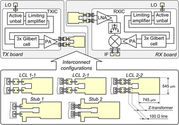
A photograph of the realized modules with two types of interconnects is shown in Fig. 2. The first interconnect is based on an LCL network realized using series bondwires and an off-chip pad acting as a shunt capacitor whereas the second interconnecting structure is matched using bondwires and differential microstrip stubs. To minimize the length of the bondwire interface, TX and RX ICs are glued in cavities.
A photograph of two pairs of realized TX and RX modules with two different bondwire compensating structures: LCL network (left figure, configuration LCL 2-1) and microstrip stub network (right figure, configuration Stub 2).

All modules use the identical differential end-fire patch antenna that has been designed in CST Microwave Studio and realized on a 127 µm thick RO3003 substrate. The size of the patch is 745 × 545 µm and its feed-point is matched to a 100 Ω differential line using an impedance transformer, which consists of two 100 µm wide microstrip lines spaced by 300 µm. To ease the bonding procedure, the copper surface is gold plated using electroless nickel immersion plating technique. The simulated return loss and the gain of the antenna across the required band are better than −10 dB and 6.9 dBi, respectively. The simulated radiation efficiency is 96%.
Compensation strategy, design and implementation of both types of differential bondwire interconnects are described in detail hereafter.
A) Differential LCL interconnect
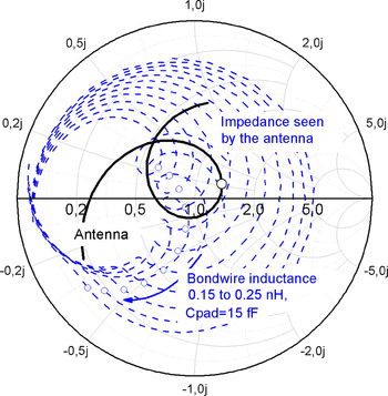
As depicted in Figs 1 and 2, the first type of interconnect consists of two bondwire bridges (gold wires with a diameter of 17 µm) with a common contact point at an intermediate off-chip pad that acts as a capacitance of 15 fF. This configuration creates an LCL T-network, which turns this interconnect into a matching structure between the output pads of the IC and the differential feed-point of the antenna. The distance between the output pads of the chip and the antenna structure is 800 µm. The estimated bondwire length at both sides of the T-network is approximately 320 µm. Very low-profile interconnects were possible thanks to the ultrasonic wedge-bonding technique and horizontal alignment of the chip pads and the off-chip metal structures. To further lower the inductance, two bondwires are used in parallel. This configuration was also simulated and the results are depicted in Fig. 3, showing the impedance seen at the interface between the LCL interconnect and the antenna with the impedance transformer for different values of the bondwire inductance across 110–150 GHz band. This figure suggests that bondwire inductances close to 0.25 nH and above might lead to significant mismatch and hence, dual wire-bonding or ribbons should be used. Although the model is based on a combination of an EM model and a simple lumped element model, it provides accurate results as demonstrated in the next section.
Matching strategy of the LCL interconnect depicting the impedance at the antenna reference plane. The blue dashed lines show the impedance across 110–150 GHz band seen by the patch antenna for different values of the bondwire inductance. Circles highlight the mid-band (130 GHz).
B) Differential interconnect with microstrip stubs
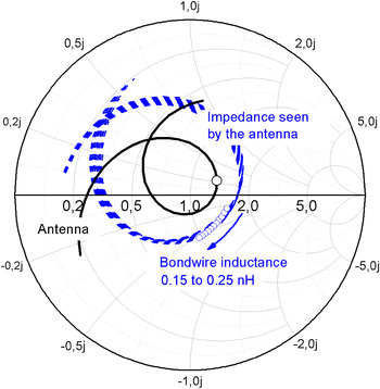
Bondwires in the second topology connect the output chip pads directly to a differential matching structure. The matching structure uses differential microstrip stubs to match the chip output together with the bondwire inductance to a 100 Ω differential line. A 500 µm long 100 Ω differential line with 100 µm slot is used to connect the antenna to the matching structure. The whole planar structure was EM simulated and optimized in CST Microwave Studio. The distance between the output pads of the chip and the compensation structure is 350 µm and the estimated length of the bondwire is 365 µm. As in the previous case, the influence of the bondwire inductance was estimated using a simple lumped element model together with the EM model of the planar compensation structure and the patch antenna. Simulation results of the impedance at the reference plane of the antenna for bondwire inductance varying from 0.15 to 0.25 nH are depicted in Fig. 4. Compared to the LCL matching network, the simulation results suggest that lower sensitivity to the variation of the bondwire inductance can be expected. The latter has been confirmed by measurements and is related to the overall length of the interconnect.
Matching strategy of the stub interconnect. As in the previous figure, matching across 110–150 GHz at the antenna reference plane is shown for different values of the bondwire inductance. Circles highlight the mid-band (130 GHz).
III. SINGLE-ENDED CHIP-TO-CHIP INTERCONNECT
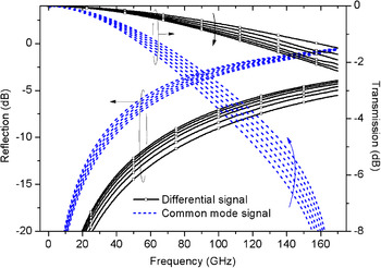
Millimeter-wave modules frequently require wideband, low-loss, and compact chip-to-chip interfaces. Compared with the differential interconnects introduced in the previous section, single-ended interface will not benefit from the virtual ground and therefore, the reactive effects of the bondwire will be more pronounced. To quantitatively estimate this inherent drawback of the unbalanced operation, two simple EM models of single-ended and differential bondwire interconnects have been built. The differential interconnect uses two coupled signal wires, whereas the single-ended interconnect uses three wires in ground-signal-ground configuration. Both interconnects have the same bondwire lengths (150 µm) and do not use any compensation. To investigate the effect of coupling between the bondwires, both structures are simulated for different spacing between bondwires, from 50 to 100 µm with a step of 10 µm. Such spacing is realistic and implementable with manual bonding. The result of this analysis is depicted in Fig. 5. It can clearly be seen that the differential interface outperforms the single ended one. For instance, at 160 GHz and spacing of 100 µm, the expected transmission loss of the differential interconnect are 3.2 dB better than the losses of the single-ended interconnect. In both cases, smaller spacing results in better performance due to the lowering of the characteristic impedance of the interconnect. The importance of the ground conductor (either the virtual one in the differential configuration or the real one in the coplanar interconnect) was also confirmed experimentally at lower frequencies in [Reference Lim, Kwon, Rieh, Kim and Hwang30].
EM simulation results of differential and single-ended interconnects (150 µm long) for different spacing between bondwires (50–100 µm with a step of 10 µm). The arrow indicates the effect of increasing the bondwire spacing. The smaller the spacing, the better the performance of both interconnects.

Common-mode excitation of the differential interconnect has been analyzed as well (both lines connected in parallel and placed in a 25 Ω environment). The results are depicted in Fig. 6. As expected, the best common mode suppression is achieved at the lowest spacing between the coupled differential lines. This is due to the fact that the mutual inductance is higher at smaller spacing, which contrary to the differential mode, adds up to the self-inductance and further increases the impedance against common mode currents.
EM simulation results of the differential interconnect under balanced and unbalanced excitation. The arrow indicates the effect of increasing the bondwire spacing. The smaller the spacing, the better the differential performance and the common mode suppression.
The aforementioned results clearly demonstrate that commonly used single-ended interconnects will require special treatment to achieve acceptable losses and matching at millimeter-wave frequencies. In this section we demonstrate that a wideband and low-loss single-ended chip-to-chip interface can be realized using short bondwires with a compensation structure. For this purpose, a simple on-chip compensation structure has been designed in the backend of a 0.13 µm BiCMOS technology. As shown in Fig. 7(a) C-L-C-L-C-L-C topology is used for the design. Two sections of thin-film microstrip lines on each chip form the required inductance (high-impedance transmission lines with dimensions 130 × 3 µm), and bond pads form the capacitance (signal pads with dimensions 50 × 50 µm and 40 × 60 µm). Ground-signal-ground bondwires form a CPW interface between two chips that are spaced by 150 µm. As in the previous case, the bondwires were realized using an ultrasonic wedge bonder. Physical dimensions, an EM model, and a chip photograph of the realized single-ended interconnect are shown in Fig. 7.
Layout, EM model built in Sonnet and a chip photograph of the realized single-ended interconnect (from left to right, respectively). All dimensions are in µm.

Figure 8 shows the EM simulation results for two compensated interconnects with bondwire lengths of 150 and 175 µm. These two values have been used to represent the actual bondwire length variation during the bonding process. EM simulation shows that the transmission loss is within 1 dB, and reflection coefficient is better than −10 dB in the entire bandwidth from DC to 170 GHz. For comparison, Fig. 8 shows simulation results of the uncompensated single-ended interconnect with 150 µm long bondwires and 80 µm spacing between wires. The influence of the spacing between the ground bondwires was investigated as well. Increasing the distance to the signal wire will lead to a decrease of the capacitance to ground of the bondwire CPW section, which will in turn increase the impedance and degrade the performance. This behavior is demonstrated in Fig. 9 and suggests that the optimum performance will be achieved for spacings from 50 to 80 µm.
EM simulation results of the compensated interconnects with 150 and 175 µm long bondwires. Results of an uncompensated interconnect with 150 µm long bondwires and 80 µm wire spacing are shown as well.

EM simulation results of the impedance of 50 Ω in series with the 175 µm long compensated interconnect for different spacing between the ground wires. For comparison, results of an uncompensated interconnect with 175 µm long bondwires and 80 µm wire spacing are shown as well.

IV. EXPERIMENTAL EVALUATION AND MEASUREMENT RESULTS
Evaluation of the designed differential and single-ended interconnects was carried out in two different ways: both differential chip-to-antenna interconnects were tested using experimental radar modules, whereas the single-ended chip-to-chip interconnect was characterized using network analyzers. Measurement techniques and results are described in the following two sections.
A) Differential chip-to-antenna interconnects
The influence of all configurations of the differential bondwire interconnects (LCL 1-1, 2-1, 2-2 and Stub 1, 2, as depicted in Fig. 1) has been evaluated with the help of an experimental 0.5 m long wireless link deploying the realized TX/RX modules. To determine the exact power applied to the interconnect of the TX module, three different samples of TX ICs were first characterized on-wafer using a waveguide F-band GSG probe connected to a spectrum analyzer via an F-band harmonic mixer extension [Reference Valenta29]. Results of the frequency response are depicted in the upper plot of Fig. 10. The maximum output power of 3 dBm (6 dBm differential) was measured at the frequency of 124 GHz. The 3-dB bandwidth is 20 GHz. Results above 140 GHz are illustrated by simulation. The conversion gain of the RX IC was determined based on on-wafer measurements of the LNA which was also designed as a separate chip, and simulation results of the designed down-converting mixer with an IF buffer. Afterwards, diced chips were glued to cavities in the Printed Circuit Board (PCB) and bonded to the dedicated on-board compensation structures.
Single-ended output power of three different TX ICs measured on-wafer and corresponding single ended IF power detected by the RX module with different interconnects at a 0.5 m distance. Link budget estimation curves do not consider losses introduced by the bondwire interconnects.
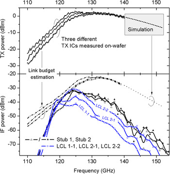
In the next step, a 0.5 m wireless link was established: two LO signals from independent signal generators were fed to the TX/RX modules. Both LOs were clocked by the same reference to avoid frequency drifting. The frequency of the LO reference sources was shifted by 1 MHz with respect to each other and simultaneously tuned from 13.75 to 19.5 GHz (which corresponds to 110–156 GHz at the wireless interface) while monitoring the 8 MHz IF at the RX output using a spectrum analyzer. The IF of 8 MHz is a result of the multiplication by eight that is performed in the TX and RX ICs. Single-ended measurement results of the IF power detected at one of the differential RX outputs for five different configurations of the bondwire interconnect are depicted in the second plot of Fig. 10.
It can be seen that compared with the LCL interconnect, the interconnect with microstrip stubs is more broadband and less susceptible to the changes of the bondwire inductance. For instance, the effect of doubling the bondwire in the stub matching network is not noticeable above 125 GHz. The main improvement of up to 7 dB is observable only in the 117–125 GHz range. The LCL interconnect, on the other hand, clearly shows the importance of the double bonding technique which can improve the link budget by up to 13 dB (LCL 1-1 vs. LCL 2-2 at 125 GHz). The latter observation is also in a good agreement with the simulation results of both types of bondwire interconnects as summarized in the previous section and is due to the fact that the bondwires in the LCL interconnect are approximately twice as long (two wired sections in a T-configuration). The influence of both matching structures on the overall radiation pattern of realized modules was investigated as well. While the LCL interconnect does not introduce any measurable influence, the matching network with microstrip stubs introduces a local minimum perpendicular to the antenna plane and splits the original single-lobe pattern into two secondary lobes. For this reason, TX/RX modules had to be tilted down toward the maximum during the measurements. This effect was expected and observed also in simulation results of far-field radiation of the whole off-chip structure. Simulation results of the radiation diagram for different lengths of the stubs are shown in Fig. 11. It can clearly be seen that the optimum length of the differential microstrip stubs for matching, which is 570 µm, does not correspond to the optimum radiation pattern. A further optimization would require involving the length and position of the stubs with respect to the radiation pattern or the use of shielded stubs.
Influence of the length of the differential matching stub on the radiation pattern. Corresponding input reflection coefficient is depicted as well.

For comparison, the second plot in Fig. 10 is also showing the estimated IF power derived from the measured TX output power, LNA gain and from the simulated antenna gain, pathloss and conversion gain of RX mixer and IF buffer. Since this estimation does not account for losses caused by the chip-to-antenna interconnects in the TX and RX modules, these losses are directly reflected in the difference between the measured and the estimated IF power. Therefore, one half of this difference represents the loss per interconnect at each module and is plotted in Fig. 12 for both LCL and stub interconnects with double bonding. The frequency response above 140 GHz is highlighted as a simulation because the TX power was not measured in this band and the link budget equation accounted for the simulated results. The 3-dB bandwidth of both types of interconnect is close to 9 GHz (117.2–126.3 GHz and 117.7–126.6 GHz for the stub and LCL interconnects, respectively). To determine the precise value of the minimum insertion loss, exact values of the variables in the link budget equation would need to be known. As a result, the minimum insertion loss is estimated using a lumped element model, which suggests the loss of 0.2 and 0.5 dB for the LCL and stub interconnects, respectively.
Loss per interconnect for both compensation topologies are derived from the IF measurement results. Measurements of completely re-packaged TX/RX modules with Stub 2 interconnects are depicted as well.
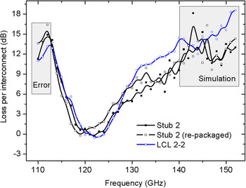
To evaluate the repeatability of the packaging and wire bonding procedures, new TX/RX modules with the differential stub interconnects were re-packaged and re-bonded using the double bonding technique. The derived loss per interconnect of the re-packaged TX/RX module is depicted in Fig. 12. Compared with the losses derived in the first module, the frequency response exhibits slightly narrower bandwidth and a shift of 1.5–2 GHz toward the lower frequencies. Considering the frequency of operation, various types of measurement errors and inaccuracies during the packaging and bonding procedures, this shift is considered insignificant (lower than 1.6%) and proves that this type of interconnect can be expected to be highly repeatable.
B) Single-ended chip-to-chip interconnect
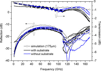
Five samples of the realized single-ended chip-to-chip interconnect were glued on a glass carrier. Three samples were left undiced, sharing the same silicon substrate, whereas two samples were diced to determine the influence of the low-resistivity silicon substrate that is located below the bondwires. All chips were bonded using manual bonding and were characterized on-wafer. S-parameter measurements were made with the help of two network analyzers, one covering the range from DC to 110 GHz (Agilent E8361A with 67–110 GHz waveguide TR modules N5620–60003) and the other one from 110 to 170 GHz (Rohde & Schwarz ZVK 24 GHz with 110–170 GHz TR modules ZVA-Z170). The measured reflection and transmission coefficients are plotted in Fig. 13. For illustration, EM simulation results are depicted as well. All samples show excellent behavior: a loss lower than 2.5 dB and a reflection coefficient better than −12 dB from DC to 170 GHz. The transmission loss at 140 GHz is around 1 dB for undiced samples and 0.75 dB for diced samples. The variation of the transmission loss is within 1 dB from DC to 170 GHz. The diced samples exhibit lower loss compared with the undiced samples due to the fact that the silicon substrate below the bondwires in the undiced case lowers the Q of the interconnect and influences also the coupling between bondwires. The diced samples achieve a bandwidth from DC to 170 GHz with a loss of 1 ± 0.5 dB. The measured performance is also in a good agreement with EM simulation results.
S-parameter measurement results of five bonded samples (three samples with and two samples without the low-resistivity Si substrate) in the frequency range from 1 to170 GHz. For comparison, simulation results are shown as well.
V. CONCLUSION
A comprehensive evaluation of compensated bondwire interconnects above 100 GHz has been carried out, addressing both, differential and single-ended interfaces.
Two types of differential compensation structures suitable for low-cost millimeter-wave chip-to-antenna interconnects were presented together with measurement results of an experimental wireless system that relies on the proposed interconnects. It has been shown that a 7.5% bandwidth and an insertion loss as low as 0.2 dB are possible in this frequency range. In comparison with other recent studies on bondwire interconnects, the bandwidth of the proposed interconnect is rather moderate. However, considering the material used, the operating frequency and namely the overall length of the second proposed interconnect (LCL connection with the overall length of 800 µm), these results are the best reported to date. It has also been demonstrated that the interconnect based on differential microstrip stubs is less sensitive to variations of the bondwire inductance and provides lower losses beyond the 3-dB bandwidth. On the other hand, the undesired shaping of the main radiation lobe due to secondary radiation of the matching stubs is the most important challenge that needs to be addressed. This undesired effect could be avoided, e.g. using a triplate or inverted microstrip structure or by optimizing the orientation of microstrip stubs at the expense of increased PCB complexity. Although only one pair of the TX/RX modules was re-packaged, re-bonded and re-measured to prove that this approach to bondwire interconnects is repeatable, it is expected that a high reproducibility of the proposed solution can be achieved. Conclusive proof of repeatability of the proposed solution is a remaining task.
Compensation of a single-ended short bondwire interconnect was investigated as well. For this purpose, a dedicated test structure has been designed and characterized up to 170 GHz. The single-ended interconnect structure shows an extremely wide bandwidth from DC to 170 GHz with a matching better than −12 dB and loss below 1 dB at 140 GHz. A very good repeatability has been obtained even with manual bonding. Preliminary simulation results suggest that a comparable performance could be achieved at even higher frequencies for scaled interconnects. This is a subject of further investigations.
It has been shown again that, if properly designed, bondwire interconnects can achieve excellent performance, competitive to other millimeter-wave interconnection techniques, at significantly lower cost. The reuse of the proposed interconnects for other applications is obvious and is not limited only to the presented scenarios. The differential chip-to-antenna interconnect could be used for example as an interconnect for balanced multi-chip systems whereas the single-ended interconnect can be integrated directly at the ICs that are to be bonded.
ACKNOWLEDGEMENTS
This work was supported by the EU project NANOTEC under the grant agreement N°288531. Authors wish to acknowledge the support of Dr. Andreas Trasser and Mr. Sven Hettich for wire-bonding the test structures and radar modules, and Mr. Christian Wipf from IHP for D-band measurements.
 Václav Valenta received his master's degree with honors from the Brno University of Technology in the Czech Republic in 2007. In 2010, he obtained a dual doctorate from the École Supérieure d'Ingénieurs en Électronique et Électrotechnique (ESIEE Paris) and the Brno University of Technology. He is currently working as an RF research fellow at the Institute of Electron Devices and Circuits in Ulm, Germany. His main research interests are focused on design of broadband microwave and millimeter-wave components for imaging and radar systems in SiGe and GaN technologies, and digital signal processing for spectrum sensing. Dr. Valenta coordinates a project on collaborative spectrum sensing funded by the German DFG agency and is responsible for scientific and management activities in different European projects.
 Thomas Spreng received his Dipl.-Ing. degree in Electrical Engineering in 2011 from Technische Universität München, Germany. Currently he is working towards his Dr.-Ing. degree at Airbus Group Innovations, Ottobrunn, Germany. His research interests are millimeter-wave MIMO radars for imaging.
 Shuai Yuan received his B.E. degree in Electronic information Engineering from Southeast University, Nanjing, China, in 2006, M.Sc. degrees in circuits and system from Southeast University and in communications technology from Ulm University, Germany in 2009, and is currently working toward the Ph.D. degree at Ulm University. From 2009 to 2010, he was with Alcatel-Lucent, Nanjing, China, where he worked on RF circuits for base stations. From 2010 to 2011 he was with ICD group, University of Twente. He is currently with the Institute of Electron Devices and Circuits, Ulm University as a member of the scientific staff and doctoral candidate. His research topics mainly involve RF/ millimeter-wave integrated circuits and systems, antenna, high performance ADCs, as well as their applications in communication and remote sensing systems. Mr. Yuan was the recipient of the EuMIC Young Engineers Prize at European Microwave Week (EuMW) 2013.
 Wolfgang Winkler is the CTO of the company Silicon Radar in Frankfurt (Oder), Germany. His main research interests are circuits for radar and wireless communication in silicon-based technologies. During the last few years he has developed integrated circuits for pulse radar systems and FMCW radar and he designed building blocks for wireless transceivers at 60 GHz and for radar circuits at different frequencies from 10 to 140 GHz. Additionally, he developed RF-ESD protection devices and designed benchmarking circuits for technology characterization and model verification. Wolfgang Winkler received the M.S. degree at the Technical University Ilmenau, Germany in 1979, and Ph.D. degree in 1984, both in Electrical Engineering.
 Volker Ziegler received his Dipl.-Ing. degree in Electrical Engineering and his Dr.-Ing. degree (with honors) both from the University of Ulm, Germany, in 1997 and 2001, respectively. From 2002 to 2003, he was a member of the ‘Knowledge Exchange Group for Research and Technology’ at the Daimler Chrysler AG in Stuttgart, Germany. During this trainee period, he was working at the University of Michigan, Ann Arbor, USA and at United Monolithic Semiconductors, Orsay, France. Afterwards, he joined AIRBUS Group Innovations, Ottobrunn, Germany, where he became an AIRBUS Expert on ‘Microwave Technologies and Systems’ in 2007. Currently, he is the Head of Team ‘RF and Waveforms’ responsible for the research performed in the field of key microwave technologies and waveforms for advanced radar and communication systems. Volker Ziegler is a member of the IEEE MTT-S Technical Coordinating Committee 21 on RF-MEMS and a member of the IEEE MTT Antennas and Propagation German Chapter Executive Board. He is an industrial advisor for the ESA Component Technical Board on Microwaves. He served twice as Associated Editor for the ‘International Journal of Microwave and Wireless Technologies’ and authored or co-authored more than 70 papers and holds nine patents.
 Dragos Dancila graduated magna cum laude as an Electrical Engineer, from Université catholique de Louvain, Belgium, in 2006 and received his Ph.D. in Applied Sciences in collaboration with IMEC, in 2011. His research includes millimeter-waves, oscillators, RF components and systems. Presently, he is a Researcher at Uppsala University, working within the Microwave group on several different topics within the microwave engineering field: (i) adaptive antennas for wake-vortex and wind RADARs, (ii) MEMS technology, and RF spectroscopy for biomedical applications such as skin cancer detection and glucose monitoring (iii) RF high power combination and generation for ESS, the European Spallation Source.
 Anders Rydberg (M’89) received his M.Sc. degree from the Lund University of Technology, Lund, Sweden, in 1976, and the Ph.D. degree from the University of Technology, Göteborg, Sweden, in 1988. He was with the National Defense Research Establishment, Stockholm, Sweden, ELLEMTEL Development Company, Ltd., Stockholm, and the Onsala Space Observatory, Onsala, Sweden, from 1977 to 1983. In 1991, he was appointed as a Docent (Associated Professor) with the Chalmers University of Technology. From 1990 to 1991, he was a Senior Research Engineer with Farran Technology Ltd., Cork, Ireland. He was with Uppsala University, Uppsala, Sweden, as a Senior Lecturer and Professor in Applied Microwave and Millimeter-Wave Technology in 1992 and 2001, respectively. He is heading the Microwave Group with the Department of Engineering Science, Uppsala University. He has been the joint-owner of Integrated Antennas AB and WISENET Holding AB, Uppsala, since 2007. He has authored and co-authored more than 220 publications in the area of micro and millimeter-wave antennas, sensors, solid-state components and circuits, and holds three patents in the areas. He has supervised seven Ph.D. students. Prof. Rydberg is an Editorial Board Member of the IEEE Microwave Theory and Techniques (MTT), the Chairman of Section D and an adjunct member of Section B of the Swedish Member Committee of URSI (SNRV), and the Chairman of the Swedish IEEE MTT/AP Chapter.
 Hermann Schumacher was born in Siegen, Germany in 1957. He received his Diplom-Ingenieur and Doktor-Ingenieur degrees in 1982 and 1986, respectively, from RWTH Aachen, Germany. From 1986 until 1990, he was a member of technical staff at Bell Communications Research (Bellcore) of Red Bank, NJ, USA. Since 1990, he has been a professor at the Institute of Electron Devices and Circuits, Ulm University, Ulm, Germany, and has been the institute director since 2010. Professor Schumacher is also the director of the university's School of Advanced Professional studies. His research interests encompass compound semiconductor devices, microwave/millimeter-wave frontend ICs, and high-frequency microsystems.


 Open access