

Introduction
The field of AlGaN-based ultraviolet (UV) optoelectronic devices (primarily emitters and photodetectors), has been an active area of research over the past two decades.[ Reference Pankove and Moustakas 1 – Reference Khan, Balakrishnan and Katona 5 ] AlGaN alloys are well suited for such devices because their energy gap can be tuned by changing the alloy composition to cover the entire UV spectral region from 210 to 360 nm. This research is motivated by a plethora of potential industrial and medical applications. Such include, for example, free-space non-line-of-sight communications, water/air/food sterilization, surface disinfection, fluorescence or Raman identification of biological/chemical agents, epoxy curing, counterfeit detection, and various diagnostic and therapeutic medical applications. However, despite intense efforts worldwide, the maximum external quantum efficiency (EQE) of fully packaged AlGaN-based deep UV-light-emitting diodes (LEDs), emitting below 300 nm, is only 1%–3%.[ Reference Khan, Balakrishnan and Katona 5 – Reference Grandusky, Gibb, Mendrick, Moe, Wraback and Schowalter 9 ] Only recently Shatalov et al. reported a UVLED emitting at 278 nm with EQE of about 10%.[ Reference Shatalov, Sun, Lunev, Hu, Dobrinsky, Bilenko, Yang, Shur, Gaska, Moe, Garrett and Wraback 10 ] This is to be contrasted with InGaN-based violet–blue LEDs, whose EQE is more than 50%.[ Reference Krames, Shchekin, Mueller-Mach, Mueller, Zhou, Harbers and Craford 11 ]
The EQE is defined as the product of the internal quantum efficiency (IQE), the injection efficiency (IE), and the extraction efficiency (EE). Thus, the poor EQE of the deep UV-LEDs may be the result of poor IQE, IE, EE, or a combination of all three factors. The IQE depends sensitively on extended and point defects, which act as non-radiative recombination centers. The IE depends on the ability to dope the n- and p-sides of the junction efficiently and to form Ohmic contacts with low contact resistivity on both sides. The EE depends sensitively on the ability to extract the light from the active region of the device to the free space.
The development of AlGaN-based UV lasers is even at an earlier stage of development. Several groups have reported the development of optically pumped deep UV lasers as well as the demonstration of stimulated emission.[ Reference Takano, Narita, Horiuchi and Kawanishi 12 – Reference Jmerik, Lutsenko and Ivanov 19 ] However, the reported shortest wavelength of electrically pumped UV lasers is 336 nm.[ Reference Yoshida, Yamashita, Kuwabara and Kan 20 ] Significant progress has been made in AlGaN-based “visible blind” or “solar blind” UV detectors to detect weak UV signals in the presence of strong ambient light in scientific research, industrial, and military applications.[ Reference Khan, Kuznia, Olson, Van Hove and Blasingame 21 – Reference Misra, Bhattacharyya and Moustakas 29 ] UV electroabsorption modulators have generally received much less attention.[ Reference Kneissl, Paoli, Kiesel, Treat, Teepe, Miyashita and Johnson 30 – Reference Kao, Bhattacharyya, Thomidis, Moldawer, Paiella and Moustakas 36 ]
In this paper, we review progress in developing UV optoelectronic devices based on AlGaN alloys grown by plasma-assisted molecular beam epitaxy (PAMBE). These include LEDs, lasers, photodetectors, electroabsorption modulators, and distributed Bragg reflectors (DBRs).
Growth, alloy ordering, and doping of AlGaN alloys
The AlGaN alloys in the form of bulk films or multiple quantum wells (MQWs) as well as device structures based on such materials were deposited by PAMBE on the c-planes of sapphire and 6H-SiC substrates. In this method, the molecular nitrogen is activated in a Veeco radiofrequency (RF) plasma source to produce active nitrogen species (atomic, ionic, and activated molecular nitrogen N2*) depending on the mode of operation.[ Reference Molnar, Singh and Moustakas 37 ] The Ga, Al, and In metals as well as Si and Mg dopants were supplied from standard effusion cells.
Fundamental problems in AlGaN films
There are a number of fundamental problems with AlGaN alloys independent of growth methods, which are responsible for the relatively low progress in developing efficient deep UV optoelectronic devices.
Due to the lack of native substrates such devices are generally grown heteroepitaxially primarily on the c-plane of sapphire and 6H- or 4H-SiC substrates. So far, sapphire has been the substrate of choice because it is inexpensive and readily available in large sizes. Furthermore, sapphire is transparent in the entire UV spectral region. To mitigate problems related to large lattice mismatch (about 13%) between AlGaN films and sapphire substrate a number of nucleation steps (conversion of the surface of sapphire from Al2O3 to AlN and the use of a low-temperature AlN buffer) have been developed to allow the annihilation of threading defects as the film grows thicker.[ Reference Moustakas, Molnar, Menon, Eddy, Moustakas, Pankove and Hamakawa 38 – Reference Amano, Sawaki, Akasaki and Toyoda 43 ] However, in spite all of these the density of threading defects is still high (~109 cm−2).
There are multiple reasons for the high density of extended and point defects in heteroepitaxially grown AlGaN films. Principle among which is the high activity of nitrogen produced either by thermal decomposition of ammonia or by plasma decomposition of molecular nitrogen.[ Reference Wright and Winkler 44 ] During epitaxial growth this active nitrogen reacts instantly with arriving Al atoms on the substrate and limits their diffusivity. This leads to the nucleation of small AlGaN islands and films with microstructures consisting of small hexagonal columnar domains. Such materials are expected to have high dislocation density, since the plurality of the threading dislocations occur primarily at the boundaries of the hexagonal columnar domains due to their incomplete coalescence.[ Reference Moustakas 45 ] Furthermore, coalescence of the small islands leads to tensile stress, which promotes the nucleation and propagation of cracks.[ Reference Nix and Clemens 46 ] This is even more important in silicon-doped high Al content AlGaN films, since silicon is an anti-surfactant and thus, it leads to microstructures with even smaller domains.[ Reference Moustakas, Liao, Kao, Thomidis, Bhattacharyya, Bhattarai and Moldawer 47 ]
Another source of the poor IQE of deep UV-LEDs is the incorporation of oxygen in AlGaN due to the high chemical affinity of aluminum for oxygen.[ Reference Elsass, Mates, Heying, Poblenz, Fini, Petroff, DenBaars and Speck 48 – Reference Moustakas and Bhattacharyya 50 ] While oxygen is a shallow donor in GaN and InGaN alloys, it is known to form DX-like centers in AlGaN alloys with high AlN mole fraction.[ Reference McCluskey, Johnson, Van de Walle, Bour, Kneissl and Walukiewicz 51 ]
Other potential problems are the poor doping efficiency of n- and particularly p-AlGaN with high AlN mole fraction, which is responsible for the poor carrier injection in the active region of the device.[ Reference Taniyasu, Kasu and Makimoto 52 ] This is due to the high ionization energies of Mg acceptors and Si-donors, which are 630 and 280 meV respectively for AlN.[ Reference Yoshida, Yamashita, Kuwabara and Kan 20 ]
Yet, another fundamental problem is the difficulty in extracting the light from deep UV-LEDs due to emission selection rules originating from changes in the valence band structure of AlGaN alloys as the AlN mole fraction in the alloy increases.[ Reference Nam, Li, Nakarmi, Lin and Jiang 53 ] Specifically, the band structure of AlGaN alloys changes as a function of AlN mole fraction due to the difference in the crystal field splitting of GaN (+38 meV) and AlN (−219 meV). As a result of the reversal of the order of the valence bands recombination in GaN leads to light polarized with the E⊥C-axis (surface emission), while in AlN the light is polarized with the E || C-axis (edge emission).
Various approaches are currently been pursued to address these problems. A number of groups are developing deep UV emitters (LEDs and lasers) by growing such devices pseudomorphically on AlN substrates.[ Reference Grandusky, Gibb, Mendrick, Moe, Wraback and Schowalter 9 , Reference Wunderer, Chua, Yang, Northrup, Johnson, Garrett, Shen and Wraback 14 , Reference Lochner, Kao, Liu, Li, Satter, Shen, Yoder, Ryou, Dupuis, Wei, Xie, Fischer and Ponce 17 ] However, such substrates are currently available in small sizes and are prohibitively expensive. Monroy et al. have employed indium as a surfactant to promote two-dimensional (2D) growth during deposition of AlGaN alloys under slightly N-rich conditions.[ Reference Monroy, Daudin, Bellet-Amalric, Gogneau, Jalabert, Brault, Barjon and Dang 54 ]
Growth mode of III-nitrides by PAMBE
Growth of AlGaN alloys by PAMBE has the potential to address some of these problems. Existing literature assumes that the growth of nitride semiconductors by PAMBE is a physical vapor phase deposition method, involving the reaction on a heated substrate of Ga-vapor with molecular nitrogen, activated first by a RF or microwave plasma. However, contrary to the growth by MBE of traditional III–V compounds (arsenides, phosphides, etc.), which takes place under group-V-rich conditions, the growth of atomically smooth GaN takes place under group-III-rich conditions of growth.[ Reference Moustakas and Molnar 55 – Reference Mula, Adelmann, Moehl, Oullier and Daudin 57 ] Growth of GaN under N-rich conditions leads to films with rough and faceted surface morphology. This is partly due to the low temperature of growth and partly because the nitrogen-activated species are highly reactive as discussed previously. Indeed theoretical studies indicate that the diffusion barrier for Ga adatoms on N-rich surface is 1.8 eV, while for Ga-saturated surface is only 0.4 eV.[ Reference Zywietz, Neugebauer and Scheffler 58 ]
The growth of GaN by PAMBE under Ga-rich condition has been addressed recently in a number of theoretical papers. First-principles total energy calculations by Northrup et al. have shown that under Ga-rich conditions the excess Ga forms a laterally contracted Ga bilayer.[ Reference Northrup, Neugebauer, Feenstra and Smith 59 ] Neugebauer et al. employed density-functional theory in combination with scanning tunneling microscopy to account for the smooth surface morphology of GaN films grown by PAMBE under Ga-rich conditions.[ Reference Neugebauer, Zywietz, Scheffler, Northrup, Chen and Feenstra 60 ] These authors demonstrated that a thin metallic film on a semiconductor surface may open an efficient diffusion channel for lateral adatom transport. Thus, adatoms may prefer diffusion within this metallic layer rather than on the top of the surface.
Our group has proposed an alternative model to account for the role of the excess Ga in the surface of the growing GaN film.[ Reference Moustakas and Bhattacharyya 50 , Reference Moustakas and Bhattacharyya 61 , Reference Moustakas and Bhattacharyya 62 ] Specifically, we have proposed that under Ga-rich conditions the GaN growth by PAMBE is a liquid phase epitaxy (LPE) rather than physical vapor deposition. In other words growth takes place through the saturation with active nitrogen of the metallic Ga at the growing surface, followed by subsequent crystallization from the melt onto the GaN seed. It should be stressed that while in traditional LPE growth the driving force is the gradient temperature between the liquid and seed, in the proposed LPE mode of MBE growth of GaN, the driving force is the concentration gradient of dissolved nitrogen in the liquid gallium due to the constant supply of active nitrogen from the plasma source.
This model assumes that the solubility of active nitrogen species is high at the low temperatures employed during growth of nitride semiconductors by MBE. The thermodynamics of GaN growth from the melt has been studied extensively by the High Pressure Institute group in Poland.[ Reference Karpinski, Jun and Porowski 63 ] The enthalpy of dissociation of molecular nitrogen is very high (9.77 eV). The molecular nitrogen adsorption on liquid Ga surface is a dissociative process and the energy barrier for this process is 5.3 eV. Due to this high-energy barrier the solubility of molecular nitrogen (N2) in Ga is only 1 at % at 1900 K. Thus, the growth of GaN from the melt usually takes place at high temperatures in order to increase the solubility of molecular nitrogen in Ga. Also, the growth takes place under high pressure of more than 15 kbar in order to prevent the decomposition of GaN at these high temperatures.[ Reference Karpinski, Jun and Porowski 63 ]
Contrary to the low solubility of molecular nitrogen, there is ample experimental evidence that active nitrogen produced by plasma decomposition of molecular nitrogen or by thermal decomposition of ammonia has a high solubility in gallium even at low temperatures. Specifically, there are reports of forming GaN by exposing liquid Ga to a nitrogen plasma at temperatures of about 700°C,[ Reference Elwell, Feigelson, Simkins and Tiller 64 – Reference Moustakas, Dismukes and Abernathy 66 ] and forming epitaxial GaN quantum dots (QDs) by exposing Ga-droplets on the sapphire substrate to ammonia or RF nitrogen plasma at similar temperatures.[ Reference Hu, Bell, Ponce, Smith and Tsong 67 , Reference Wang, Ozcan, Sanborn, Ludwig, Bhattacharyya, Chandrasekaran, Moustakas, Zhou and Smith 68 ] From the various active nitrogen species the metastable molecular nitrogen (N2*) is expected to have the higher solubility in Ga since its internal energy is 9.5 eV[ Reference Wright and Winkler 44 ] and thus, its energy barrier to adsorption to Ga should be very small. On the other hand, the solubility of atomic nitrogen in Ga may be limited since Ga can catalyze the recombination of atomic nitrogen to form molecular nitrogen. Thus, the N2* radicals are the species, which contribute mostly to the GaN growth at these low temperatures.
While the growth of GaN under Ga-rich conditions has been extensively investigated both theoretically and experimentally, the growth of AlGaN under Ga-rich conditions raises the issue of how the excess Ga in the surface of the AlGaN film affects the film stoichiometry. The kinetics of growth of AlGaN alloys by PAMBE has previously reported by Iliopoulos and Moustakas.[ Reference Iliopoulos and Moustakas 69 ] These authors reported that the stoichiometry of the films depends only on the ratio of the [Al] to active [N] fluxes ([Al]/[N]) and not by the ratio of [Al]/[Ga] fluxes as it is the case in AlGaAs.[ Reference Moustakas 70 ] This is due to the much stronger Al–N bond versus the Ga–N bond. Thus, any excess gallium during growth accumulates on the surface of the growing AlGaN film in the form of liquid gallium, but it does not affect the film stoichiometry. In the presence of excess Ga in the surface of the growing AlGaN films the growth proceeds via LPE as discussed previously. In other words, the arriving active nitrogen species, Al atoms, as well as intentional or unintentional impurities dissolve first in the liquid Ga and incorporate into the AlGaN film from the liquid phase.
The growth of AlGaN by PAMBE under Ga-rich conditions has a number of beneficial effects in the optoelectronic quality of these films. This growth mode is likely to lead to lateral compositional inhomogeneities due to statistical fluctuations of the thickness of the liquid Ga on the surface of the growing AlGaN film. These compositional inhomogeneities lead to band-structure potential fluctuations, which are sufficiently deep that lead to exciton localization even at room temperature. This prevents the carriers from diffusing to point or extended defects and to recombine non-radiatively.[ Reference Bhattacharyya, Moustakas, Zhou, Smith and Hug 71 ] Another source of band-structure potential fluctuations is the partial alloy ordering, which is discussed below.
Also, in the proposed LPE growth mode the incorporation of impurities in the AlGaN film requires that their solubility in Ga at the growth temperature to be relatively high. We have reported previously that the concentration of impurities such as O, H, and C is in the 1019 cm−3 range when the GaN films are grown under nitrogen-rich conditions, while they are two to three orders of magnitude less when the films are grown under Ga-rich conditions.[ Reference Moustakas and Bhattacharyya 50 , Reference Moustakas and Bhattacharyya 62 ] The reduction in oxygen incorporation can be accounted for by the formation of volatile gallium oxides, which would then desorb. Similarly hydrogen may form volatile gallium hydrides. Regarding the reduction in carbon impurities one has to assume that the solubility of carbon in Ga must be very low, since gallium carbides compounds are not known to exist. The incorporation of dopant impurities such as Si and Mg is discussed below.
It is important to stress that in general the LPE growth process has been successfully treated as a thermodynamic process.[ Reference Pearsall 72 ] A thermodynamic analysis of Al incorporation in GaN toward the formation of AlGaN during MBE growth of nitride semiconductors under metal-rich conditions was presented by Hoke et al.[ Reference Hoke, Torabi, Mosca and Kenedy 73 ] As discussed previously the active nitrogen dissolves in the liquid Ga in the surface of the film and incorporates in the GaN seed from the liquid phase. If simultaneously Al atoms arrive on the substrate, then the incorporation of Al is favored, if the Gibbs free energy at the growth temperature (ΔG T) of the reaction in Eq. (1) is negative.
 $${\rm Al} + {\rm GaN}\, \to {\rm AlN} + {\rm Ga},{\rm} \Delta G^{\rm T}\, \lt \,0.$$
The Gibbs free energies of formation at 1000 K for a number of relevant compounds and elements are given in Table I of Ref. Reference Hoke, Torabi, Mosca and Kenedy73. Using these values we find ΔG T = −209.6 kJ/mole and thus, this reaction is strongly thermodynamically favorable. Therefore, Al will preferentially incorporate into the growing nitride film despite the excess Ga in the surface. As discussed previously, this is in agreement with the findings in Ref. Reference Iliopoulos and Moustakas69, that the composition of Al x Ga1−x N alloys is determined by the ratio of the incoming Al flux to the reactive nitrogen flux [Al]/[N]. In the limit of [Al] = [N] pure AlN film will grow despite the excess Ga in the surface of the growing film.
Alloy ordering in AlGaN films
The phenomenon of long-range atomic ordering has been observed in a wide range of III–V semiconductor alloy systems.[ Reference Zunger, Mahajan and Moss 74 ] The most studied case of ordering is probably the CuPt-type in the alloy system GaInP.[ Reference Gomyo, Suzuki and Iijima 75 ] In an ideally ordered case, instead of a random Ga0.5In0.5P alloy, a (GaP)1(InP)1 superlattice (SL) is formed spontaneously in the [111]-direction during growth on the (001) plane. Long-range atomic ordering in cubic III–V alloys is found to be driven by surface phenomena and not by bulk thermodynamics.[ Reference Su, Ho and Stringfellow 76 ] In the case of cubic III–V alloys, theoretical calculation and experimental evidence attribute the phenomenon to specific surface reconstructions caused by subsurface strain.[ Reference Osorio, Bernard, Froyen and Zunger 77 ] Such reconstructions arrange adatoms on the surface {001} planes in such a way that a SL is created along the {111} planes, when these adatoms are subsequently buried. The formation of the ordered phase affects both the alloy optical[ Reference Gomyo, Suzuki and Iijima 75 ] and electronic properties.[ Reference Friedman, Zhu, Kibbler, Olson and Moreland 78 ]
Long-range atomic ordering in AlGaN films grown by PAMBE on the c-plane of sapphire and 6H-SiC substrates were first reported by Korakakis et al.[ Reference Korakakis, Ludwig and Moustakas 79 ] Al x Ga1−x N alloys crystallize in the wurtzitic, hexagonal close-packed structure. The geometrical structure factor for a Bragg reflection (hkl) in such crystals is given by the expression:
 $$F_{hkl} = f_{\rm A} + f_{\rm B}{\kern 1pt} {\rm exp[}2\pi i[(h + 2k)/3 + l/2]{\rm ],}$$
where f A and f B are the average scattering factors of the Al, Ga atoms occupying the (000) and (1/3, 2/3, 1/2) sublattice sites of the hexagonal cell, respectively. In Eq. (2), we have omitted the scattering from the nitrogen atoms since their presence does not affect the discussion related to cation ordering. When the two sites are occupied by the same atomic species or by a random mixture of the two species, Bragg reflections with l = odd and h + 2k = 3n are forbidden according to Eq. (2). Thus, in pure GaN, pure AlN, and random Al x Ga1−x N alloys, the (0001), (0003), etc. diffractions are forbidden. However, if one of the sublattice sites is preferentially occupied by Al or Ga in an Al x Ga1−x N alloy, the two terms no longer cancel and SL peaks result.
An example of such an x-ray diffraction (XRD) was reported by Iliopoulos et al.[ Reference Iliopoulos, Ludwig and Moustakas 80 ] and is shown in Figure 1 for an Al0.65Ga0.35N grown by PAMBE on the c-plane of sapphire. Apart from the allowed (0002) AlGaN and (0006) sapphire peaks, the reflections at the (0001) and the (0003) AlGaN reciprocal space points are present. It is important to note that such experimental data cannot be attributed to stacking faults in the films, since the geometrical structure factor for reflections with indices h = k = 0 are independent of the basal plane coordinates of the atoms in the unit cell and therefore cannot probe the stacking sequence of planes. Instead the (0001) and (0003) peaks are a direct indication of the presence of 1 × 1 ordering in the crystal. Also to rule out atomic ordering due to vacancies or strain we have confirmed the long-range atomic ordering in these films by polarization-dependent EXAFS.[ Reference Woicik, Ludwig and Moustakas 81 ]
On-axis XRD scan of an Al0.55Ga0.45N film grown by RF PAMBE.[ Reference Iliopoulos, Ludwig and Moustakas 80 ]

In contrast to the case with the cubic arsenides and phosphides, the ordering reported in the wurtzite nitride alloys occurs along the [0001] growth direction. Therefore the mechanisms that induce ordering in the arsenides and phosphides would appear not to be applicable in the nitrides. Theoretical and experimental investigations of the formation mechanism(s) for ordering in the nitrides have been limited. However, a model to explain simple 1 × 1 ordering with alternating Ga- and Al-rich layers, has been proposed by Northrup et al.[ Reference Northrup, Romano and Neugebauer 82 ]
In addition to 1 × 1 atomic ordering, Iliopoulos et al. have reported complex ordering in the nitrides along the [0001] growth direction, with periodicities of several wurtzite unit cells.[ Reference Iliopoulos, Ludwig and Moustakas 80 , Reference Iliopoulos, Ludwig, Moustakas and Chu 83 , Reference Iliopoulos, Ludwig, Moustakas, Komninou, Karakostas, Nouet and Chu 84 ] This differs qualitatively from the 1 × 1 ordering discussed previously, which does not alter the fundamental structural repeat distance along the c-direction. An example of such complex ordering structure is shown in Figure 2. Figure 2(a) is the on-axis θ–2θ XRD spectra for three c-plane Al x Ga1−x N films grown by PAMBE on the c-plane sapphire for differing group-III beam equivalent pressure (BEP) values. Here the BEP is the sum of the Al and Ga fluxes, while their ratio was held fixed (BEPAl/BEPGa = 0.53). In particular, samples A, B, and C were grown with III/V flux ratios of 1.0, 0.9, and 0.6, respectively. As measured by RBS, the final compositions of the films were x = 0.89 for sample A, x = 0.74 for sample B, and x = 0.55 for sample C.[ Reference Iliopoulos, Ludwig, Moustakas and Chu 83 ] Otherwise the three samples were grown with identical nucleation and growth conditions.
(a) On-axis XRD for three AlGaN films grown with different ratios of III/V fluxes; (b) SAD pattern of the AlGaN film A.[ Reference Iliopoulos, Ludwig, Moustakas and Chu 83 ]

Sample C, which was grown under N-rich conditions of growth, shows the (0001) diffraction peak characteristic of the simple 1 × 1 ordered structure discussed above. However, the films grown under group-III-rich conditions show a number of additional SL peaks indicating the presence of a SL structure with different periodicity.
Film A of Figure 2(a) was also studied by transmission electron microscope (TEM) selected area diffraction (SAD). The SAD pattern in Figure 2(b) shows the same SL peaks observed by the XRD in Figure 2(a). In taking the data described in Figure 2(b) the zone axis 〈11–20〉 was tilted toward the 〈10–10〉 direction to avoid any double diffraction.[ Reference Iliopoulos, Ludwig, Moustakas, Komninou, Karakostas, Nouet and Chu 84 ]
As discussed by Iliopoulos et al.,[ Reference Iliopoulos, Ludwig, Moustakas and Chu 83 ] the XRD and TEM data of sample A can be accounted for by the presence of two spontaneously formed SL structures in the film: a dominant one having a period of 14-ML and a secondary one having a period of 12-ML.
However, Wang et al.[ Reference Wang, Ozcan, Ludwig, Bhattacharyya, Moustakas, Zhou and Smith 85 ] reported that Al0.72Ga0.28N films grown in environments with group-III/N ratios >1 exhibit ordered SL structures that are incommensurate with the wurtzite crystal lattice. The increasing complexity of the ordering with increasing Ga-rich growth environment suggests that the ordering is related to the presence of a Ga overlayer.
Other groups have also reported the existence of complex ordered structures,[ Reference Behbehani, Piner, Liu, El-Masry and Bedair 86 , Reference Ruterana, De Saint Jores, Laugt, Omnes and Bellet-Amalric 87 ] but with repeat distances of 3, 4, and 6 monolayers, sometimes coexisting in a single sample. In these references, the films were grown by the metalorganic chemical vapor deposition (MOCVD) method, suggesting that this type of complex ordering in nitride alloys is universal and depends sensitively on growth conditions.
It should be stressed that the observed atomic ordering in both AlGaN and InGaN alloys is only partial.[ Reference Korakakis, Ludwig and Moustakas 79 ] In other words, some domains are atomically ordered and some are random.[ Reference Doppalapudi, Basu and Moustakas 88 ] Also, since the energy gap of the alloy was found to depend on the degree of ordering,[ Reference Iliopoulos 89 ] partial atomic ordering introduces band-structure potential fluctuations, which may have an effect on the performance of the optoelectronic devices as discussed below.
Doping
Silicon and magnesium are the primary n- and p-type dopants in GaN and its alloys with AlN and InN.
N-type doping
There are multiple reports that the conductivity in these n-type doped alloys decreases drastically with AlN mole fraction. For example, in unintentionally n-type doped AlGaN alloys grown by MOCVD, Lee et al.[ Reference Lee, Gershenzon and Goldenberg 90 ] reported a rapid decrease in conductivity for AlN mole fraction higher than 40%. McCluskey et al.[ Reference McCluskey, Johnson, Van de Walle, Bour and Kneissl 91 ] attributed the unintentional n-type conductivity to oxygen impurities. Bremser et al.,[ Reference Bremser, Perry, Zheleva, Edwards, Nam, Parikh, Aspnes and Davis 92 ] using also the MOCVD method, have doped AlGaN alloys with silicon up to AlN mole fraction of 42%. However, additional silicon resulted in highly resistive films. Taniyasu et al.[ Reference Taniyasu, Kasu and Kobayashi 93 ] reported that AlGaN films containing more than 3 × 1019 cm–3 of silicon become highly resistive due to self-compensation of silicon donors. Skierbiszewski et al.[ Reference Skierbiszewski, Suski and Leszczynski 94 ] studied AlGaN films with AlN mole fraction between 50% and 60% under high pressure. These authors concluded that the Si dopant forms two donor states: one of them is shallow and has an effective mass character; the other is strongly coupled to the crystal lattice and thus, forms a deeper state. They also argued that this metastable localized state is the source for persistent photoconductivity in high Al concentration AlGaN alloys. Stampfl et al.[ Reference Stampfl and Van de Walle 95 ] concluded, based on density-functional-pseudopotential calculations, that the experimentally observed decrease in n-type conductivity for AlN mole fraction more than 40% has two potential origins: (a) for auto-doped films (doped unintentionally with oxygen) the reduction in conductivity is due to a DX transition that converts the shallow donor into deep level; (b) in the case of silicon the reduction of conductivity is due to cation vacancies. The Cornell and the Ohio State groups[ Reference Hwang, Schaff, Eastman, Bradley, Brillson, Look, Wu, Walukiewicz, Furis and Cartwright 96 , Reference Bradley, Goss and Brillson: 97 ] have reported significant progress in doping AlGaN alloys with silicon by PAMBE. Specifically, they were able to dope AlGaN alloys with 80% AlN mole fraction to a level of 8.5 × 1019 cm–3 electron concentration.
The incorporation of Si in nitride semiconductors should follow the thermodynamic analysis, which was discussed previously.[ Reference Hoke, Torabi, Mosca and Kenedy 73 ] According to this model the incorporation of Si in GaN and AlN can be determined from Eqs. (3) and (4), using the Gibbs free energies from Ref. Reference Hoke, Torabi, Mosca and Kenedy73.
 $${\rm Si} + {\rm 4/3GaN} \to {\rm 1/3S}{\rm i}_{\rm 3}{\rm N}_{\rm 4}{\rm + 4/3Ga,}$$
 $${\rm \Delta} G^{{\rm 1000 \,K}}{\rm =} {\rm -} {\rm 134}{\rm. 7 \,kJ}/{\rm mole,}$$
 $${\rm Si} + {\rm 4/3AlN}\, \to {\rm 1/3S}{\rm i}_{\rm 3}{\rm N}_{\rm 4}{\rm + 4/3Al,}$$
 $${\rm \Delta} G^{{\rm 1000 \,K}} = + 144{\rm. 7 \,kJ}/{\rm mole}{\rm.} $$
As pointed out in Ref. Reference Hoke, Torabi, Mosca and Kenedy73 these equations do not imply that a Si3N4 molecule exists on the surface of the growing film but that the strength of the Si–N bonds in the film is reflected in the free energy of formation of this molecule. Based on these thermodynamic arguments, under Ga-rich growth conditions Si should incorporate and dope GaN n-type. On the other hand, under Al-rich conditions Si cannot incorporate in AlN. Doping of AlN with Si was reported only during growth of AlN under N-rich conditions.[ Reference Hermann, Futmayr, Bargmaier, Dollinger, Stutzmann and Eickoff 98 ]
Our group has reported the degenerate n-type doping with Si by PAMBE of AlGaN films up to 80% AlN mole fraction.[ Reference Xu., Thomidis, Friel and Moustakas 99 ] Figure 3 shows the dependence of carrier concentration and electron mobility on AlN mole fraction. The Si cell temperature during growth of these films was kept at constant temperature.
The dependence of (a) carrier concentration and (b) electron mobility on AlN mole fraction in Si-doped AlGaN films grown by PAMBE.[ Reference Xu., Thomidis, Friel and Moustakas 99 ]

P-type doping
The doping of GaN and its alloys p-type with Mg cannot be done easily under N-rich conditions because at the growth temperatures of GaN of about 700 °C the vapor pressure of Mg is more than 10 Torr and thus, the sticking coefficient of Mg will be extremely small.[ Reference Bhattacharyya, Li, Cabalu, Moustakas, Smith and Hervig 100 ] According to the thermodynamic model, based on Eq. (5), Mg should readily incorporate into GaN under Ga-rich conditions of growth.
 $${\rm Mg} + {\rm 2/3GaN} \to {\rm 1/3M}{\rm g}_{\rm 3}{\rm N}_{\rm 2}{\rm + 2/3Ga,}$$
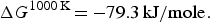 $${\rm \Delta} G^{{\rm 1000 \,K}}\,{\rm =} \,{\rm -} {\rm 79}{\rm. 3 \,kJ}/{\rm mole}{\rm.} $$
Bhattacharyya et al. demonstrated efficient p-doping of GaN with Mg when growth takes place under Ga-rich conditions.[ Reference Bhattacharyya, Li, Cabalu, Moustakas, Smith and Hervig 100 ] Figure 4 shows the resistivity versus Mg cell temperature for two series of p-GaN films grown at 770 °C.[ Reference Bhattacharyya, Li, Cabalu, Moustakas, Smith and Hervig 100 ]
Resistivity versus Mg cell temperature for two families of p-GaN films grown as discussed in the text.[ Reference Bhattacharyya, Li, Cabalu, Moustakas, Smith and Hervig 100 ]
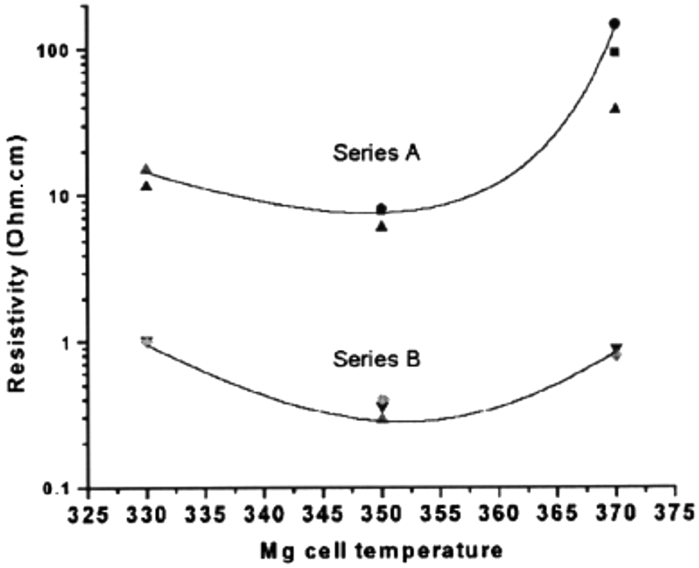
As indicated in Figure 4, the one series of p-GaN films was grown under Ga-rich conditions, while the second one was grown under stoichiometric conditions. The poorer incorporation efficiency of Mg in GaN grown under stoichiometric conditions was attributed to the low sticking coefficient of Mg as discussed previously. On the other hand, during growth under Ga-rich conditions the Mg dissolves in the liquid gallium on the surface of GaN and incorporates from the liquid phase. Based on this argument GaN can be doped more efficiently p-type with Mg under Ga-rich conditions at higher temperatures, since the solubility of Mg in Ga is higher.
A number of p-GaN films were grown under Ga-rich conditions in our laboratory and their transport coefficients were evaluated by Hall Effect measurements. As shown in Figure 5, the hole mobility versus hole concentration follows the expected monotonic relation.
Mobility versus carrier concentration for a number of p-GaN films grown under Ga-rich conditions.

As discussed previously the p-doping with Mg of AlGaN films with high AlN mole fraction is limited by the high ionization energy of Mg acceptors. An alternative approach to improve the doping efficiency of AlGaN is to dope the material in the form of an Al x Ga1−x N/Al y Ga1−y N SL.[ Reference Li 101 ] The concept of SL doping was first proposed in 1990 by Suemune to improve the acceptor doping efficiency in II–VI compounds.[ Reference Suemune 102 ] These calculations predicted a hole concentration for the SL a factor of five higher than that of the bulk ZnSe films. In 1999, a number of groups have applied the concept to doping with Mg of AlGaN/GaN SLs and reported an order of magnitude higher hole concentration than the corresponding AlGaN films with the same average composition.[ Reference Kozodoy, Hansen, DenBaars and Mishra 103 – Reference Goepfert, Schubert, Osinsky, Norris and Faleev 105 ] Figure 6 shows the resistivity versus AlN mole fraction for bulk AlGaN films and Al x Ga1−x N/Al y Ga1−y N SLs grown by our group using PAMBE.[ Reference Li 101 ] It is obvious from these data that SL doping is far more efficient.
Resistivity versus average AlN mole fraction for Mg-doped bulk AlGaN films and Al x Ga1−x N/Al y Ga1−y N SLs.[ Reference Li 101 ]

Development of AlGaN QWs with high IQE
As discussed previously there are a number of potential advantages of growing AlGaN alloys by PAMBE under excess Ga. In this section, we are investigating of how this growth mode affects the IQE of AlGaN MQWs, which are the active regions of UV-LEDs and lasers. Bhattacharyya et al. investigated the effect of the excess liquid-Ga on the IQE of AlGaN films by growing a series of identical in thickness and composition Al0.70Ga0.30N/AlN MQWs on the c-plane of sapphire substrates and studying their photoluminescence (PL) efficiency as a function of temperature.[ Reference Bhattacharyya, Moustakas, Zhou, Smith and Hug 71 ] Specifically, during the growth of the wells the flux of Ga was varied from that corresponding to stoichiometric conditions (III/V ~ 1) to (III/V ≫ 1). The thickness of the barriers and wells were 6 and 1.5 nm, respectively.
The normalized luminescence spectra of these samples are presented in Figure 7. These data show that all MQW samples exhibit only a sharp near band-edge emission. It is important to stress that although the thicknesses and compositions of the wells and barriers were the same for all samples, the emission wavelengths varies from 225 to 250 nm as the Ga-flux increased from III/V close to one to much greater than one. This red shift of the PL spectra for these identical MQWs indicates that the excess Ga during the growth of the wells introduces band-structure potential fluctuations whose depth increases with the amount of excess Ga. Consistent with this interpretation is also the increase of the spectral width from 11 to 16 nm. These potential fluctuations are much deeper than the statistical ones due to alloy disorder and thus, they can cause carrier localization and efficient radiative recombination even at room temperature. The origin of these band-structure potential fluctuations are either compositional inhomogeneities due to statistical fluctuations of the thickness of Ga covering the surface of the growing AlGaN film or are due to partial alloy ordering as discussed previously.
Room-temperature luminescence from Al0.7Ga0.3N/AlN MQWs, with identical well and barrier widths as described in the text.[ Reference Bhattacharyya, Moustakas, Zhou, Smith and Hug 71 ]

The IQE of these MQWs was determined by measuring the PL spectra as a function of temperature. We define the IQE at room temperature as the ratio of the integrated PL intensity at room temperature divided by that at 10 K.[ Reference Chichibu, Uedono, Onuma, Haskell, Chakraborty, Koyama, Fini, Keller, Denbaars, Speck, Mishra, Nakamura, Yamaguchi, Kamiyama, Amano, Akasaki, Han and Sota 106 ] This definition assumes that the recombination at 10 K is radiative, which is a reasonable assumption. The IQEs for the samples discussed in Figure 7 are presented in Figure 8. Thus, the IQE for these MQWs varies from 5% for emission at 225 nm, to 50% for emission at 250 nm. This increase in the IQE for identical Al0.7Ga0.3N/AlN MQWs is attributed to the localization of the excitons due to band-structure potential fluctuations introduced during the growth of the wells under Ga-rich conditions.
Room-temperature IQE of the Al0.70Ga0.30N/AlN MQWs described in Figure 7.[ Reference Bhattacharyya, Moustakas, Zhou, Smith and Hug 71 ]

Our group also investigated the growth and properties of AlGaN MQWs emitting in the deep UV on the c-plane of 6H- and 4H-SiC substrates.[ Reference Zhang, Nikiforov, Thomidis, Woodward, Sun, Kao, Bhattarai, Moldawer, Zhou, Smith and Moustakas 107 ] Growth of AlGaN alloys and QWs on SiC for emitters has several advantages. The lattice mismatch between SiC and AlN is only ~1%. Other advantages include the high thermal conductivity of SiC compared with that of sapphire, as well as the ability to form facets by cleaving. Simultaneously, the growth of AlGaN on SiC substrates has a number of challenges, principal among which are the accidental nitridation of the SiC substrate prior to the epitaxial growth and the formation of stacking mismatch boundaries at the step edges due to the polytype difference between 2H-AlGaN and 6H- or 4H-SiC.[ Reference Doppalapudi, Moustakas and Nalwa 108 ] Zhang et al. reported that such AlGaN/AlN MQWs emitting at 245 nm have an IQE of 68%.[ Reference Zhang, Nikiforov, Thomidis, Woodward, Sun, Kao, Bhattarai, Moldawer, Zhou, Smith and Moustakas 107 ]
These values of IQE for AlGaN MQWs emitting at 250 nm are comparable with those of InGaN MQWs.[ Reference Chichibu, Uedono, Onuma, Haskell, Chakraborty, Koyama, Fini, Keller, Denbaars, Speck, Mishra, Nakamura, Yamaguchi, Kamiyama, Amano, Akasaki, Han and Sota 106 ] In the case of InGaN QWs, the high IQE is generally attributed to band-structure potential fluctuations due to compositional inhomogeneities in these alloys. The origin of these compositional inhomogeneities is phase separation by spinodal decomposition due to the 11% difference in the ionic radius of In and Ga atoms in tetrahedral sites. On the other hand, such phase separation is not expected in AlGaN alloys since Al and Ga atoms have identical ionic radius. Thus, we believe that the band-structure potential fluctuations in these alloys are the result of the growth mode under excess Ga as discussed earlier.
UV-LEDs
The majority of the UV-LEDs reported in the literature were produced by the MOCVD method.[ Reference Khan, Balakrishnan and Katona 5 – Reference Shatalov, Sun, Lunev, Hu, Dobrinsky, Bilenko, Yang, Shur, Gaska, Moe, Garrett and Wraback 10 ] The MBE method has a number of advantages in developing such devices. As discussed earlier this method has the ability to introduce band-structure potential fluctuations in the active region of the device, which promote efficient radiative recombination. Furthermore, it can prevent the incorporation of certain undesirable impurities such as oxygen, carbon, and hydrogen, and also it can facilitate the incorporation of dopant impurities such as Mg and Si. In this section, we report the progress made in developing such devices by PAMBE. Our group initially developed efficient UV-LEDs emitting in the 340–350 nm as well as methods of growing such devices on textured GaN templates to improve both the IQE and EE.[ Reference Cabalu, Bhattacharyya, Thomidis, Moustakas and Collins 109 , Reference Cabalu, Thomidis, Friel, Moustakas and Riyopoulos 110 ]
More recently, in a series of papers Liao et al. reported for the first time the development of mW power deep UV-LEDs grown by MBE on sapphire substrates.[ Reference Liao, Thomidis, Kao, Moldawer, Zhang, Chang, Nikiforov, Bellotti and Moustakas 111 – Reference Liao, Kao, Thomidis, Moldawer, Woodward, Bhattarai and Moustakas 114 ] The epilayer structure of the investigated deep UV-LED devices, is schematically shown in Figure 9.
Schematic representation of the epitaxial design of the deep UV-LEDs investigated.[ Reference Liao, Thomidis, Kao, Moldawer, Zhang, Chang, Nikiforov, Bellotti and Moustakas 111 ]

The AlN template was approximately 2 µm thick. A 10-period AlGaN/AlN strain management SL was grown on to the AlN template before the growth of the Si-doped n-AlGaN cladding layer. Such strain management SL has been proved to be effective in accommodating the elastic strain induced by Si incorporation into the AlGaN lattice and to prevent cracking.[ Reference Romano, Van de Walle, Ager, Gotz and Kern 115 , Reference Zhang, Wang, Gaevski, Chen, Fareed, Yang, Simin and Asif Khan 116 ] The electron concentration of the Si-doped n-AlGaN was of the order of mid-1018 cm−3. The active region consisted of a single asymmetric AlGaN/AlGaN quantum well (QW) and a 10-nm AlGaN electron-blocking layer (EBL) heavily doped with Mg. The thickness of the barrier close to n-AlGaN layer was 10 nm, while the other barrier next to EBL was 3 nm. Such an asymmetric design was chosen in order to balance the electron and hole injections into the QW due to differences in diffusion lengths of holes and electrons.[ Reference Mayes, Yasan, McClintock, Shiell, Darvish, Kung and Razeghi 117 ] The composition and thickness of the EBL were optimized in order to best block electron overflow into the p-type region. The AlGaN QW was grown under Ga-rich conditions to allow for the formation of band-structure potential fluctuations. The final structure is capped by a p-AlGaN layer and p-GaN contact layer. The Al composition of the various layers was varied depending of the intended emission wavelength of the device. Ohmic contacts to n-AlGaN were made using vanadium-based alloys whose contact resistivity was reported previously to be 10−6 Ω/cm2 for AlN mole fraction up to 70%.[ Reference France, Xu, Chen, Chandrasekaran and Moustakas 118 – Reference Pookpanratana, France, Félix, Wilks, Weinhardt, Hofmann, Tati Bismaths, Mulcahy, Kronast, Moustakas, Bär and Heske 121 ]
Liao et al. demonstrated the dependence between IQE and band-structure potential fluctuations by studying the optical absorption and the PL spectra of two identical Al0.5Ga0.5N/Al0.65Ga0.35N MQWs, grown under different amount of excess Ga.[ Reference Liao, Thomidis, Kao and Moustakas 113 ] The one MQW was grown under Ga-rich conditions (III/V > 1, MQW-1) and the second was grown under stoichiometric conditions (III/V~1, MQW-2). The results are shown in Figure 10. From these data we have estimated the IQE of MQW-1 to be 32% and that of the MQW-2 to be 15%. The inset of Figure 10 shows the derivative of the optical absorbance obtained from transmission measurements from these MQWs and their RT PL spectra. The peak of the derivative of the absorption constant at 275 nm is a measure of the optical gap of the Al0.5Ga0.5N.[ Reference Moustakas, Pankove and Moustakas 41 ] As seen from this data the peak of the PL spectra at 300 nm is red shifted from the optical band edge by 25 nm (376 meV). Such large Stokes shift is another evidence of band-tail states due to potential fluctuations. In contrast, the Stokes shift of MQW-2 is only 15 nm (233 meV). The correlation between IQE and Stokes shift of the two samples grown with and without excess Ga clearly establishes that excess Ga during AlGaN growth leads to pronounced potential fluctuation and band-tail states, which contributes to carrier localization and enhance radiative recombination.
Plot of integrated PL intensity versus inverse temperature of MQW-1 and MQW-2; inset shows derivative of absorbance of samples MQW-1 and -2, and their RT emission spectra.[ Reference Liao, Thomidis, Kao and Moustakas 113 ]

Figure 11 shows the normalized electroluminescence (EL) spectra for a number of UV LEDs grown in our laboratory by PAMBE.[ Reference Liao, Kao, Thomidis, Moldawer, Woodward, Bhattarai and Moustakas 114 ]
Normalized EL spectra of UV-LEDs emitting from 320 to 265 nm, produced by PAMBE.[ Reference Liao, Kao, Thomidis, Moldawer, Woodward, Bhattarai and Moustakas 114 ]

Figure 12 shows the performance characteristics of an unpackaged device emitting at 273 nm.[ Reference Liao, Thomidis, Kao and Moustakas 113 ] Figure 11 shows the electroluminescence (EL) spectra under pulsed injection up to 100 mA. The inset of Figure 11 shows the integrated optical power output and EQE under both DC and pulsed injection. Heating limits the performance of the device who's EQE under DC injection is 0.4%. The low EQE is partly due to heating and partly due to low light extraction of about 1%–2%. To increase the light extraction it will be required to remove the sapphire substrate and texture appropriately the nitride film.
EL spectra of a UV-LED emitting at 273 nm measured under pulsed injection at 10% duty cycle. Inset shows the integrated optical power output under DC and pulsed injection as well as the calculated EQE of the device.[ Reference Liao, Thomidis, Kao and Moustakas 113 ]

UV lasers
As discussed earlier several groups have reported the development of prototype optically pumped AlGaN-based deep UV lasers as well as demonstrated stimulated emission.[ Reference Takano, Narita, Horiuchi and Kawanishi 12 – Reference Jmerik, Lutsenko and Ivanov 19 ] In 2004, Takano et al. reported the first evidence of lasing at 241.5 nm under pulsed optical pumping with a threshold pumping power approximately 1200 kW/cm2 at room temperature.[ Reference Takano, Narita, Horiuchi and Kawanishi 12 ] In 2010, Jmerik et al. reported the first MBE grown device lasing at 303 nm.[ Reference Jmerik, Mizerov, Sitnikova, Kop'ev, Ivanov, Lutsenko, Tarasuk, Rzheutskii and Yablonskii 13 ] After that a number of groups reported optically pumped lasers fabricated on AlN substrates with relatively lower threshold power density.[ Reference Wunderer, Chua, Yang, Northrup, Johnson, Garrett, Shen and Wraback 14 , Reference Lochner, Kao, Liu, Li, Satter, Shen, Yoder, Ryou, Dupuis, Wei, Xie, Fischer and Ponce 17 ]
The employment of MQW structures is one of the most effective approaches for obtaining lasing. However, homogeneous QWs require high-carrier density to invert their population before any stimulated emission process sets in. As discussed previously, our group has developed by PAMBE AlGaN/AlN MQWs emitting below 250 nm with high IQE on both sapphire and SiC substrates.
For evaluating the optical gain of these MQWs Pecora et al. investigated two different AlGaN MQW structures grown on the Si face of 6H-SiC substrates.[ Reference Pecora, Zhang, Nikiforov, Zhou, Smith, Yin, Paiella, Dal Negro and Moustakas 16 , Reference Pecora, Zhang, Nikiforov, Yin, Paiella, Dal Negro and Moustakas 18 ] A schematic of the two samples is shown in Figure 13. In both structures, first a 500-nm-thick AlN cladding layer was grown followed 10 periods of AlGaN MQWs consisting of 1.5 nm wells and 40 nm barriers. The first MQW (sample A), shown in Figure 13(a), consists of Al0.6Ga0.4N wells and Al0.9Ga0.1N barriers, while the second MQW, shown in Figure 13(b) consists of Al0.7Ga0.3N wells and AlN barriers (sample B). The AlGaN QWs in both samples were grown under Ga-rich conditions. During growth of sample A, a flux of indium has also been employed. Both structures were capped with a 100-nm-thick AlN layer for wave guiding. The number of QWs was selected to optimize the tradeoff between vertical optical confinement and material gain for fixed number of injected carriers.[ Reference Chuang 122 ]
A schematic of the investigated AlGaN MQW samples.[ Reference Pecora, Zhang, Nikiforov, Yin, Paiella, Dal Negro and Moustakas 18 ]

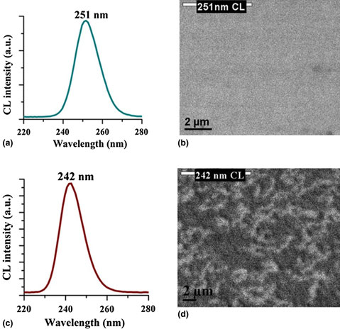
The emission properties of these structures were investigated using cathodoluminescence (CL) spectroscopy and mapping. Figure 14 shows the CL spectra and monochromatic CL maps for the two samples described in Figure 13. The striking difference between the two samples is that the sample, grown under Ga-rich conditions but in addition an indium flux, has a spatially homogeneous emission, while the sample grown only under Ga-rich conditions the monochromatic CL map reveals spatial non-uniformities on a submicron scale, consistent with the previously discussed formation of clustering and band-structure potential fluctuations in AlGaN alloys grown by the discussed method.
CL spectra and corresponding monochromatic CL maps for the two samples described in Figure 12.[ Reference Pecora, Zhang, Nikiforov, Yin, Paiella, Dal Negro and Moustakas 18 ]

The microstructure of the sample B was investigated by TEM.[ Reference Pecora, Zhang, Nikiforov, Zhou, Smith, Yin, Paiella, Dal Negro and Moustakas 16 ] High-angle annular-dark-field images were recorded with a probe size of ~0.2 nm, using a JEOL JEM-2010F operated in scanning TEM mode at 200 kV. Figure 15 shows a high-angle annular-dark-field (Z-contrast) electron micrograph cross-section of the same sample. The enlarged image reveals nanocluster-like features within the AlGaN layer. The typical size of the nanoclusters in this image is approximately 2 nm in the plane and 1.5 nm (the well thickness) in the growth direction, suggesting QD behavior. However, given the high-magnification (i.e., small spatial extent) of this micrograph and the longer-range inhomogeneities observed in Figure 14, we are unable to estimate the actual density and average size of these nanoclusters. Further structural studies will, therefore, be required to fully characterize the possible role of 3D quantum confinement in these samples.
(a) High-angle annular-dark-field (Z-contrast) electron micrograph showing cross-section of AlN/AlGaN sample, and (b) enlarged image revealing cluster-like features within AlGaN layer.[ Reference Pecora, Zhang, Nikiforov, Zhou, Smith, Yin, Paiella, Dal Negro and Moustakas 16 ]

The optical gain properties of these MQWs were investigated and reported in a series of papers by Pecora et al.[ Reference Pecora, Zhang, Nikiforov, Zhou, Smith, Yin, Paiella, Dal Negro and Moustakas 16 , Reference Pecora, Zhang, Nikiforov, Yin, Paiella, Dal Negro and Moustakas 18 , Reference Pecora, Zhang, Yin, Paiella, Dal Negro and Moustakas 123 ] The variable-stripe length (VSL) methodology has been used for a detailed quantification of the gain properties.[ Reference Shaklee, Nahory and Leheny 124 – Reference Röwe, Vehse, Michler, Gutowski, Heppel and Hangleiter 128 ] The reader is referred to the original papers by Pecora et al. for the details of the measurements and data analysis. In here we only present a summary of these data.
Deep-UV, 150 fs laser pulses at 220 nm were used to optically pump the MQW structures. The pump laser is focused on the sample surface through a cylindrical lens forming a stripe whose length can be monitored and adjusted through a blade mounted in a motorized computer-controlled stage. The beam profile along the stripe has been measured through the knife-edge technique, resulting in a height of the stripe of 5 µm and a maximum stripe length of 250 µm, which provides a homogeneous illumination of the sample. In the VSL setup, the samples were characterized by exciting the top surface and collecting the amplified spontaneous emission from the cleaved edge of the sample.[ Reference Pecora, Zhang, Yin, Paiella, Dal Negro and Moustakas 123 ]
The edge emission of the two samples, discussed in Figures 13 and 14, as a function of the pump fluence is shown in Figure 16. The measured spectrum intensity is divided by the excitation fluence in order better emphasize the nonlinear behavior of the emission. The spectra in Figure 16(a) correspond to sample A. The emission from this sample is sub-linear with the fluence, demonstrating absorption in this structure. On the other hand, the spectra in Figure 16(b), which correspond to the sample B, have the opposite behavior. As the pump fluence increases the signal intensity strongly increases with a clear superlinear trend demonstrating optical gain in this structure.
Edge emission as a function of the wavelength for the sample with homogeneous wells (a) and with strong band-structure compositional fluctuations (b). Data are scaled by the excitation fluence.[ Reference Pecora, Zhang, Nikiforov, Yin, Paiella, Dal Negro and Moustakas 18 ]

The spectra of Figure 16(b) were fitted as single Gaussian functions to determine the peak position and the full-width half-maximum (FWHM) of the emission and the data are plotted as a function of pumping fluence in Figure 17. Black dots refer to the left side axis, which reports the energy corresponding to the peak position. Red squares are relative to the right axis, which represents the FWHM of the spectra. As the pump fluence increases, the edge emission narrows and blue-shifts. In particular, the FWHM decreases from 12.5 to 8.5 nm, while the peak position shifts up from 5.00 to 5.09 eV. The superlinear emission along with the blue shift and the spectral narrowing of this sample are strongly supporting the onset of stimulated emission in this sample.
Peak position (black dots, left-side axis) and FHWM (red circles, right-side axis) of the edge emission spectra from the sample with compositional fluctuations as a function of the pump fluence.[ Reference Pecora, Zhang, Nikiforov, Yin, Paiella, Dal Negro and Moustakas 18 ]

On the other hand, we have conducted a similar analysis on the sample grown in the presence of indium, and found no changes in the peak position and the spectral width. This is consistent with the observed sub-linear trend of the measured edge emission with the pump fluence. As discussed earlier indium was found to be a surfactant during growth of AlGaN under slightly nitrogen-rich conditions of growth.[ Reference Monroy, Daudin, Bellet-Amalric, Gogneau, Jalabert, Brault, Barjon and Dang 54 ] On the other hand, this sample was grown under Ga-rich conditions. One possibility is that the Indium dissolves in the liquid Ga in the surface of the growing AlGaN film and forms Ga–In liquid solution,[ Reference Sun, Pecora, Woodward, Smith, Dal Negro and Moustakas 129 ] which wets better the AlGaN seed than pure liquid Ga and forms a uniform in thickness Ga–In liquid film covering the AlGaN seed. Thus, Al and active nitrogen dissolving into the liquid Ga-In film lead to laterally homogeneous AlGaN film.
Pecora et al. have also investigated the polarization properties of the edge emission of both samples in order to better understand the origin of the observed luminescence and gain.[ Reference Pecora, Zhang, Yin, Paiella, Dal Negro and Moustakas 123 ] The polar plot of Figure 18, shows the peak intensity measured for both samples as a function of the analyzer angle. Red square dots correspond to the structure A, while blue circles are relative to the structure B. 0° corresponds to the transverse-magnetic (TM) and 90° to the transverse-electric (TE) polarizations. Intensities have been recorded at the highest pump fluence (60 µJ/cm2) and they are reported in a linear scale. First, we observe that the sample with compositional fluctuations is about a factor of five brighter than the other. More importantly, the emission from the homogeneous wells is totally unpolarized, while the compositional fluctuations introduce a different band order resulting in strongly TE polarized ASE.
Measured peak intensity for the sample with (black dots) and without (red circles) compositional fluctuations as a function of the analyzer angle.[ Reference Pecora, Zhang, Nikiforov, Yin, Paiella, Dal Negro and Moustakas 18 ]

The Al content in this sample is sufficiently high (70%), and a turnover from the TE to the TM polarization is expected for an Al-content of 60%–80%, depending on the thickness of the well and on the strain in the active layer.[ Reference Northrup, Chua, Yang, Wunderer, Kneissl, Johnson and Kolbe 130 – Reference Park 133 ] Since the wells in our structure are very thin, it is reasonable that the TE polarization is still predominant.
Using the VSL method Pecora et al.[ Reference Pecora, Zhang, Nikiforov, Yin, Paiella, Dal Negro and Moustakas 18 ] have also determined the gain coefficient from the evolution of the peak-emission intensity as a function of the optically pumped sample length and from these data they obtained the absorption/gain spectrum for the two samples and the data are shown in Figure 19. Red squares correspond to the structure A. The spectrum appears to be featureless and always negative in values, as expected for an absorbing 1D waveguide, and it represents a measure of the net modal absorption coefficient of the material. The introduction of compositional fluctuations in the samples dramatically modifies the gain spectrum. Blue circles are mostly in the positive side of the graph, indicating that the sample is driven well in the amplification regime. On the longer wavelength side of the spectrum, the measured data turn into negative values. The wavelength of zero gain is at 266 nm (4.66 eV), which represents an experimental estimation of the effective band gap of the material. We notice that this effective gap value should not be confused with the estimated gap of a homogeneous material for the nominal Al content.
Absorption/gain spectra measured at the highest pump fluence for the sample with (blue dots) and without (red circles) compositional fluctuations.[ Reference Pecora, Zhang, Nikiforov, Yin, Paiella, Dal Negro and Moustakas 18 ]

The data of Figure 19 clearly demonstrate optical gain in AlGaN MQWs with band-structure potential fluctuations down to 230 nm with a maximum net modal gain value of 120 cm−1. The optical gain threshold was measured to be 5 µJ/cm2 from which we estimate the density of optically excited carriers at the threshold to be 1.4 × 1017 cm−3. This is two orders of magnitude lower than what can be achieved with homogeneous QW structures,[ Reference Pecora, Zhang, Nikiforov, Yin, Paiella, Dal Negro and Moustakas 18 ] which highlights the benefits of introducing band-structure potential fluctuations in the MQW layers for laser applications.
Recently, our group has also proposed the fabrication of deep-UV lasers based on AlGaN alloys in the form of a graded-index separate confinement heterostructure (GRINSCH), as schematically shown in Figure 20.[ Reference Sun, Pecora, Woodward, Smith, Dal Negro and Moustakas 129 , Reference Sun, Woodward, Yin, Moldawer, Pecora, Nikiforov, Dal Negro, Paiella, Ludwig, Smith and Moustakas 134 – Reference Pecora, Sun, Dal Negro and Moustakas 136 ] Such laser device structures were successfully used in traditional III–V compounds and were found to have the lowest threshold current. Besides the efficient carrier and optical field confinement in lasers based on the GRINSCH configuration, such laser designs based on AlGaN alloys have the additional advantage of automatically leading to a p–n junction formation,[ Reference Sun, Woodward, Yin, Moldawer, Pecora, Nikiforov, Dal Negro, Paiella, Ludwig, Smith and Moustakas 134 ] owing to opposite compositional grading of the AlGaN alloys in either side of the active region of the device.[ Reference Jena, Heikman, Green, Buttari, Coffie, Xing, Keller, DenBaars, Speck, Mishra and Smorchkova 137 ] Thus, such an AlGaN laser structure has the potential to overcome the difficulties associated with the efficient doping of AlGaN alloys. Stimulated emission and optical gain in these devices was also demonstrated.[ Reference Pecora, Sun, Dal Negro and Moustakas 136 ] The crystal microstructure and optical properties of such GRINSCH devices can be found in the original papers.[ Reference Sun, Pecora, Woodward, Smith, Dal Negro and Moustakas 129 , Reference Sun, Woodward, Yin, Moldawer, Pecora, Nikiforov, Dal Negro, Paiella, Ludwig, Smith and Moustakas 134 – Reference Pecora, Sun, Dal Negro and Moustakas 136 ]
Schematic representation of the investigated GRINSCH double heterostructure.[ Reference Sun, Woodward, Yin, Moldawer, Pecora, Nikiforov, Dal Negro, Paiella, Ludwig, Smith and Moustakas 134 ]

Photodetectors
The extremely strong absorption and radiation-induced aging effects in most semiconductor materials has historically hampered the development of high-quantum-efficiency semiconductor UV detectors. AlGaN-based UV detectors, unlike those based on traditional semiconductors such as silicon and gallium arsenide, are making strides in detecting UV radiation—from 400 nm to x-rays, as well as alpha particles—with improved sensitivity, high spectral selectivity, and low noise. With these advances, nitride-based UV detectors are finding use in areas such as the detection of UV flames for combustion control, surveillance of rockets and intercontinental ballistic missiles, secure space-to-space communication, detection of UV scintillation for medical imaging, monitoring of pollutants such as nitrous oxide and sulfur dioxide in the ionosphere, in space-based instrumentation for UV astronomy and in UV photolithography for semiconductor processing. As shown in Figure 21, the AlGaN-based material system is well suited for UV photodetectors because its direct band gap can be tuned from 360 to 200 nm by changing the alloy composition, enabling true visible-blind or solar-blind detectors.[ Reference Khan, Kuznia, Olson, Van Hove and Blasingame 21 – Reference Misra, Bhattacharyya and Moustakas 29 ] Excellent reviews on UV photodetectors were presented in Refs Reference Razeghi and Rogalski23, Reference Monroy, Calle, Pau, Muñoz, Omnès, Beaumont and Gibart26.
The optical transmission spectra of Al x Ga1−x N thin films as a function of composition x.[ Reference Misra, Bhattacharyya and Moustakas 29 ]

Semiconductor UV detectors can be made to operate either in the photoconductive or the photovoltaic mode. The photovoltaic detectors can have the form of a Schottky barrier, p–i–n diode, avalanche photodiode, heterojunction phototransistor, or charge-coupled devices.[ Reference Razeghi and Rogalski 23 , Reference Monroy, Calle, Pau, Muñoz, Omnès, Beaumont and Gibart 26 ]
Photoconductive detectors are fabricated from AlGaN alloys in thin-film form with interdigitated metal contacts placed on the surface of the material to maximize light transmission while minimizing transit time. These photoconductive detectors, as opposed to photovoltaic ones, exhibit the important advantage of internal gain, which reduces the requirement for low-noise preamplifiers. The gain is due to the fact that the minority carriers are trapped while the majority carriers go around the circuit many times before recombination. Of course the fundamental principle in all detectors is that the gain times the bandwidth should be constant. Thus, if the detector is designed to have high photoconductive gain, its response time is long. The photoconductive gain is given by the expression:
 $$G = \mu \tau V/d^2 = \tau /t_{\rm r}.$$
Here, μ is the electron mobility, τ is the carrier lifetime, V is the applied bias voltage, d is the inter-electrode spacing, and t r is the carrier transit time. Thus, the gain in photoconductive detectors occurs because the recombination lifetime is much longer than the transit time. As a result, while the gain depends on the dimensions of the device and the applied voltage, the (μτ) product—determined from the gain measurements—is the real figure of merit of the material.
The values of the photoconductive gain and responsivity of AlGaN UV detectors, reported by various groups, were found to vary widely.[ Reference Khan, Kuznia, Olson, Van Hove and Blasingame 21 – Reference Misra, Bhattacharyya and Moustakas 29 ] To find the origin of this variation, we fabricated a number of UV photoconductive detectors from GaN of varying resistivity and AlGaN of various compositions and determined the (μτ) product from the gain measurements.[ Reference Misra, Korakakis, Ng and Moustakas 25 , Reference Moustakas and Misra 28 , Reference Misra and Moustakas 138 ] Figure 22 shows the (μτ) product for the fabricated GaN and AlGaN photoconductive detectors.[ Reference Moustakas and Misra 28 ] It is evident from these data that the (μτ) product in these photodetectors varies by many orders of magnitude and is a strong function of resistivity of the semiconductor. Thus, by using GaN or AlGaN, UV detectors can be fabricated with either high gain/low speed, or vice versa.[ Reference Moustakas and Misra 28 ]
The mobility-lifetime product (μτ) in Al x Ga1−x N and GaN photodetectors varies with film resistivity.[ Reference Misra, Korakakis, Ng and Moustakas 25 , Reference Moustakas and Misra 28 ]

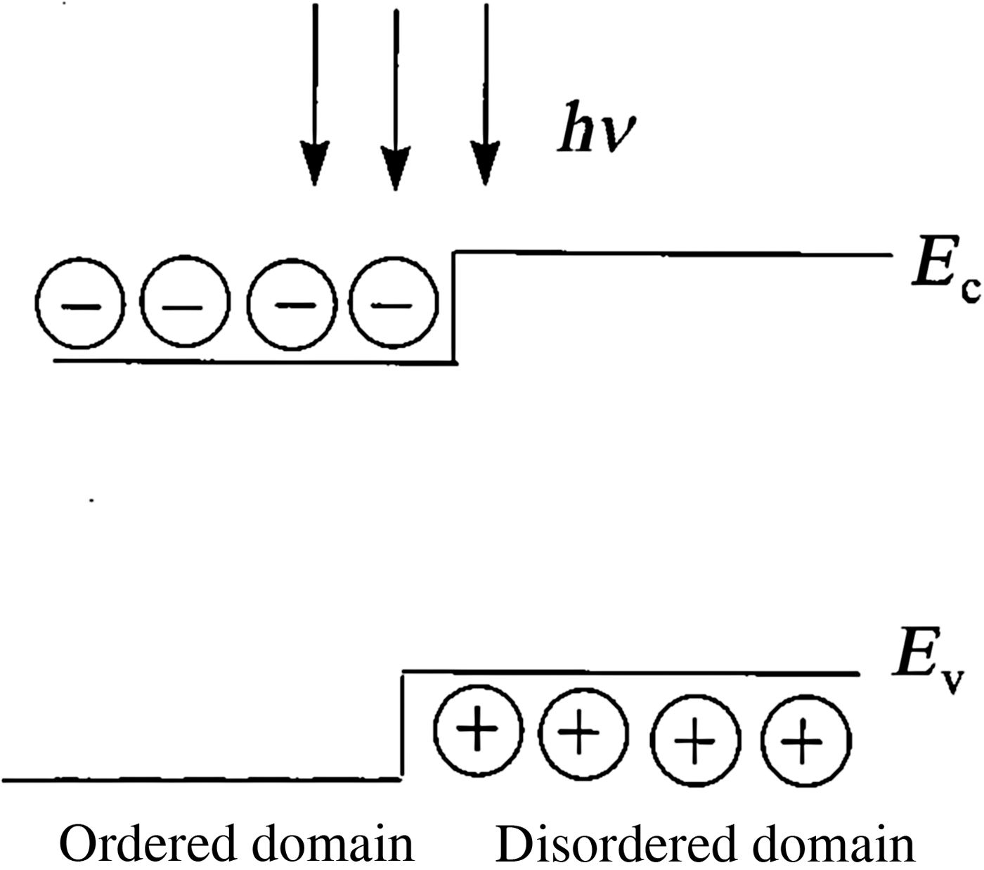
The data in Figure 22 indicate that AlGaN photodetectors have higher (μτ) products than GaN ones, even though they are expected to have lower mobility than GaN because of alloy scattering and shorter lifetime than GaN because of their more defective nature. To account for this anomaly our group investigated the structure of the AlGaN alloys and found that these materials consist of domains that are atomically ordered and others that have random alloy structure (partial ordering ordering).[ Reference Korakakis, Ludwig and Moustakas 79 ] Based on this finding we have proposed[ Reference Misra, Korakakis, Ng and Moustakas 25 ] that the band-structure of the ordered and random domains form a type-II heterostructure as shown in Figure 23. Thus, the electron–hole pairs created by the illumination are separated in the ordered and random domains, which lead to the observed enhancement of the lifetime. This hypothesis was later supported by atomistic empirical pseudopotential simulations reported by Dudiy and Zunger.[ Reference Dudiy and Zunger 139 ] These authors found that the band alignment between random and ordered domains changes from types I to II at about 40% AlN mole fraction in the AlGaN alloys.
Schematic illustration of the potential band alignment of ordered and disordered domains in the Al x Ga1−x N alloys.[ Reference Misra, Korakakis, Ng and Moustakas 25 , Reference Moustakas and Misra 28 ]
Optical modulators
Electroabsorption modulators are semiconductor electro-optic devices in which a change in absorption coefficient is induced by an externally applied electric field. Such devices based on cubic III–V semiconductors have been the subject of extensive research over the past three decades and have found a variety of applications in, e.g., fiber-optic data transmission, photonic switching, and optical interconnects. In general, particularly strong modulation can be obtained when the absorption edge is dominated by excitonic effects, due to the sharp nature of the resulting absorption features.
However, in smaller-band gap bulk semiconductors such as GaAs the room temperature exciton-binding energy (~4 meV) is substantially less than the thermal energy k B T at room temperature. As a result, the excitonic nature of the absorption edge at room temperature is not obvious due to thermal broadening, and the associated benefits for electroabsorption modulation are lost. On the other hand, the exciton-binding energy becomes substantially larger in QW structures, leading to well-resolved excitonic absorption peaks even at room temperature. High-performance optical modulators have therefore been developed over the years based on the quantum confined Stark effect in QWs,[ Reference Chemla, Miller, Smith and Dingle 140 ] where large changes in the excitonic resonance are obtained through the application of an electric field along the growth direction.
Research in the area of electroabsorption modulators based on wurtzite III-nitride semiconductors is still in the very early stage of development.[ Reference Kneissl, Paoli, Kiesel, Treat, Teepe, Miyashita and Johnson 30 – Reference Kao, Bhattacharyya, Thomidis, Moldawer, Paiella and Moustakas 36 ] In these materials, strong electric fields are already present in the QWs due to spontaneous and piezoelectric polarizations; as a result, an even greater change in absorption is achievable, especially if the internal fields are compensated by the external bias so that the net field in the QWs is reduced. Such devices are likely to find a number of applications. Of particular interest is their development for non-line-of-sight free-space optical communications based on atmospheric light scattering where the use of short-wavelength radiation is advantageous due to its large scattering cross-section. External optical modulators in these systems would allow for higher transmission rates, without the deleterious transient heating effects that are typically associated with direct current modulation of semiconductor light sources. Nitride electroabsorption modulators, incorporated within a laser cavity, have also been used for the generation of short pulses of visible/UV radiation via Q-switching.[ Reference Kneissl, Paoli, Kiesel, Treat, Teepe, Miyashita and Johnson 30 ]
A basic property of nitride semiconductors that is particularly important in this context is provided by their large exciton-binding energies (about 25 meV in GaN and even higher in ternary AlGaN alloys). This is a direct consequence of the heavy electron and hole effective masses of these materials, which in turn are directly related to their large band gap energies. As a result, even in bulk samples at room temperature the optical absorption edge is dominated by excitonic effects, so that strong electroabsorption of near band gap radiation can be expected.
Electroabsorption modulators based on bulk GaN films
A UV optical modulator based on a 0.4-μm-thick GaN film grown by MOCVD has been reported by Oberhofer et al.[ Reference Oberhofer, Muth, Johnson, Chen, Fleet and Cooper 31 ] However, this device was found to require a prohibitively large applied voltage (>80 V) to produce any appreciable change in transmission. Specifically a maximum modulation depth under normal-incidence operation of 18% at 305 V bias was reported.
Our group reported[ Reference Kao, Bhattacharyya, Thomidis, Paiella and Moustakas 35 ] the development of a GaN electroabsorption modulator grown by RF PAMBE with similar active layer thickness and device geometry with dramatically improved performance over that reported in Ref. Reference Oberhofer, Muth, Johnson, Chen, Fleet and Cooper31 A schematic of the investigated device is shown in Figure 24. Following nitridation of the sapphire surface, a relatively thick (0.5 µm) AlN film was initially grown in this structure, so that all subsequent epitaxial layers are under compressive strain which reduces their probability of developing cracks. A transparent contact layer consisting of Si-doped n-Al0.16Ga0.84N was then deposited, followed by a nominally intrinsic Al0.3Ga0.7N film whose function is to electrically isolate the GaN active region from the bottom contact layer. The active region is also nominally undoped (with an estimated density of unintentional donor impurities of about 1017 cm−3) and has a nominal thickness of 0.4 µm.
Schematic cross-sectional view of the bulk GaN optical modulator.[ Reference Kao, Bhattacharyya, Thomidis, Paiella and Moustakas 35 ]

The electroabsorption devices shown in Figure 24 were fabricated by standard photolithography and inductively coupled plasma etching in chlorine. Ohmic contacts to n-Al0.16Ga0.84N were formed using the multilayer structure Ti/Al/Ni/Au and transparent Schottky contact was formed on the GaN active region using Ni/Au.
Prior to the device fabrication, the material optical absorption spectrum was determined via transmission measurements at room temperature and the results are plotted in Figure 25.[ Reference Kao, Bhattacharyya, Thomidis, Paiella and Moustakas 35 ] These data clearly show that even without cryogenic cooling the absorption edge of this bulk sample is dominated by excitonic effects, leading to a sharp peak at a photon energy of about 3.47 eV. The abrupt increase in absorption at about 3.7 eV is due to the 1-μm-thick Al0.16Ga0.84N film.
Absorption spectrum of the epitaxial material used to fabricate the device shown in Figure 24.[ Reference Kao, Bhattacharyya, Thomidis, Paiella and Moustakas 35 ]

The normal-incidence transmission spectra under different reverse bias conditions were measured and the data are shown in Figure 26.[ Reference Kao, Bhattacharyya, Thomidis, Paiella and Moustakas 35 ] The measured transmission spectra at various reverse bias voltages from 0 to 14 V through the device were then normalized to similarly measured transmission spectra through a sapphire substrate. As the applied voltage is increased, the excitonic absorption resonance is broadened and quenched, leading to an increase in transmission near the exciton peak and to a decrease in transmission at sufficiently detuned photon energies. From these data we obtain a maximum modulation depth M of about 30% at a photon energy of about 3.45 eV, where M is defined as the ratio [T(V)−T(0)]/T(0) and T(V) is the device transmission as a function of bias voltage V.
Normalized transmission spectra through a bulk GaN for different values of the applied reverse bias voltage from 0 to 14 V in steps of 2 V. The inset shows a zoom-in of those traces near the excitonic resonance.[ Reference Kao, Bhattacharyya, Thomidis, Paiella and Moustakas 35 ]

The measured transmission spectra can also be used to calculate the corresponding changes in absorption coefficient Δα(V) = α(V)–α(0) versus photon energy, for different values of the applied voltage. Specifically, since T(V) is proportional to exp[−α(V)d], where d is the thickness of the absorbing layer (0.4 µm in this case), we can calculate Δα(V) from Eq. (7).
 $$\Delta \alpha {\rm (}V{\rm )} = - 1/d{\rm} \left\{ {{\rm ln}\left[ {T\left( V \right)/T\left( 0 \right)} \right]} \right\}.$$
Several spectra of Δα obtained with this procedure are shown in Figure 27.[ Reference Kao, Bhattacharyya, Thomidis, Paiella and Moustakas 35 ] The maximum change in absorption coefficient here is found to increase with applied voltage up to a peak (absolute) value of about 7 × 103 cm−1 at V = 12 V. As the reverse bias is further increased, a non-negligible amount of leakage current begins to flow across the active layer. This leads to a thermal modulation of the band edges via resistive heating, which tends to compensate the field-induced changes in the absorption edge. As a result, no further increase in Δα is obtained at higher voltages.
Differential absorption spectra for a bulk GaN modulator for different values of the applied reverse bias voltage from 0 to 14 V in steps of 2 V.[ Reference Kao, Bhattacharyya, Thomidis, Paiella and Moustakas 35 ]

Electroabsorption modulators based on GaN/AlGaN MQWs
A UV optical modulator based on GaN/AlGaN MQWs, was first reported by Friel et al.[ Reference Friel, Thomidis and Moustakas 32 ] This modulator structure was grown by RF PAMBE on (0001) sapphire and is shown schematically in Figure 28. The modulator active region consisted of 10 periods of Al0.17Ga0.83N/GaN QWs, nominally undoped. The well and barrier widths were designed to be 50 and 40 Å, respectively. Devices were fabricated using standard photolithographic techniques. Mesa structures were formed by inductively coupled plasma etching using chlorine. A Schottky contact was formed directly on top of the QWs using a thick Pt/Au pad on one corner of the mesa and thin Pt/Au semi-transparent contact over the remainder of the mesa surface. The external field across the QWs was controlled by applying a reverse bias to the Schottky contact. For group-III-polar materials this leads to a compensation of the internal fields in the QWs.
Schematic of a UV optical modulator structure based on GaN/Al0.17Ga0.83N MQWs.[ Reference Friel, Thomidis and Moustakas 32 ]

Figure 29 shows the optical transmission through the device as a function of reverse bias. The inset shows the transmission over an extended energy range. At photon energies below 3.4 eV, thin-film interference fringes can be observed. The attenuation of light between about 3.4 and 3.7 eV is due to absorption in the QWs and the absorption edge at about 3.75 eV is due to the Al0.17Ga0.83N:Si cladding layer. The observed changes in the transmission spectra with increasing reverse bias are attributed to enhancement of the excitonic absorption in the QWs.
Optical transmission spectra through the modulator device as a function of applied reverse bias. The insert shows the spectra over an extended photon energy range for 0 and −10 V bias.[ Reference Friel, Thomidis and Moustakas 32 ]

The optical transmission data in Figure 29 were used to calculate the change in the absorption coefficient in the QWs Δα due to the applied bias. Since the transmission T(V) at a bias voltage V is proportional to e −α(V)d , where d is the thickness of the absorbing layer (total thickness of the QW layers), Δα (V) = α (V)−α (0), is given by Eq. (7) and plotted in Figure 30. A clear enhancement of the excitonic resonance with increasing reverse bias can be seen at about 3.48 eV.
Change in the absorption coefficient of the optical modulator as a function of applied bias.[ Reference Friel, Thomidis and Moustakas 32 ]

Focusing on the main excitonic resonance at about 3.48 eV in Figure 30, we note that the induced change in the absorption coefficient is around one order of magnitude larger than that of typical III-arsenide or III-arsenide-phosphide electroabsorption modulators, for comparable bias voltages,[ Reference Chemla, Miller, Smith and Dingle 140 ] demonstrating the great potential for using these devices in non-linear optical applications. The observed order of magnitude increase in Δα(V) in comparison to that of other III–V materials is simply a reflection of the greater near-band-edge absorption coefficient in III-nitrides of about 105 cm−1 in relation to, for example, III-arsenides of about 104 cm−1.
Distributed Bragg reflectors
Our group also reported progress in developing DBRs based on AlGaN alloys by PAMBE.[ Reference Ng, Doppalapudi, Iliopoulos and Moustakas 141 – Reference Brummer, Nothern, Nikiforov and Moustakas 145 ] The efficiency of UV optoelectronic devices can improve significantly if they are designed in a resonant cavity form, such as resonant cavity LEDs, vertical-cavity surface-emitting lasers, resonant cavity detectors, and asymmetric Fabry–Perot electroabsorption modulators.[ Reference Yan, Simes and Coldren 146 ] Such resonant cavity devices require high reflectivity DBRs. Honda et al. have estimated the threshold current density in a GaN VCSEL structure and concluded that an increase in the peak reflectance of the DBR mirror from 90% to 99% results in more than an order of magnitude reduction in the threshold current density.[ Reference Honda, Katsube, Sakaguchi, Koyama and Iga 147 ]
Another important requirement for the fabrication of nitride resonant cavity devices is the large bandwidth of the primary reflectance peak. This is important because the active region of the nitride devices is based on alloy heterostructures or MQWs, whose optical properties are very sensitive to small variations in growth or process parameters. As we have discussed earlier AlGaN and also InGaN[ Reference Doppalapudi, Basu, Ludwig and Moustakas 148 ] alloys can develop compositional inhomogeneities and various types of alloy ordering depending on growth parameters. Such phenomena affect their optical properties resulting in spectral shift of their absorption edge and emission spectra.
The main difficulty in fabricating nitride DBRs with high reflectivity and large bandwidth is the small index of refraction contrast that can be obtained within the entire AlGaN alloy composition. A number of groups have reported the fabrication of AlGaN/GaN DBRs with peak reflectance in the near ultraviolet to blue-green region of the spectrum.[ Reference Asif Khan, Kuznia, Van Hove and Olson 149 – Reference Langer, Barski, Simon, Pelekanos, Konovalov, Andre and Dang 151 ] With the employment of 30–40 quarter wave periods, peak reflectivities at 390 nm of 96% were obtained with a bandwidth of about 14 nm.[ Reference Someya and Arakawa 150 ] A similar device was reported to have peak reflectance of 96% at 460 nm with a bandwidth of 22 nm.[ Reference Langer, Barski, Simon, Pelekanos, Konovalov, Andre and Dang 151 ]
DBRs based on AlN/GaN quarter wave stacks have the potential for higher peak reflectance and larger bandwidth with approximately half the number of quarter wave periods. Such DBRs were reported early on by our group using PAMBE[ Reference Ng, Doppalapudi, Iliopoulos and Moustakas 141 – Reference Ng and Moustakas 143 ] and the Sandia group using gas source MBE.[ Reference Fritz and Drummond 152 ] The cross-section TEM micrograph of a DBR stack consisting of 20.5 periods of AlN/GaN with thickness of 62.3 and 40.3 nm, respectively, is shown in Figure 31.[ Reference Moustakas, Iliopoulos, Sampath, Ng, Doppalapudi, Misra, Korakakis and Singh 153 ] The reflectivity spectra of this DBR structure is also shown in the inset along with simulation results based on the transmission matrix method. The peak reflectance of 99% occurred at a center wavelength of 465 nm and the reflectance bandwidth is 45 nm. Such DBRs have been fabricated for maximum reflectance from the near UV to the green part of the spectrum. Details regarding the DBRs as well as a prototype VCSEL structure have been published elsewhere.[ Reference Ng, Moustakas and Chu 142 , Reference Ng and Moustakas 143 ]
Cross-section TEM micrograph of a 20.5 period AlN/GaN DBR stack. Inset shows experimental reflectivity spectra from this DBR along with simulation results based on the transition matrix method.[ Reference Moustakas, Iliopoulos, Sampath, Ng, Doppalapudi, Misra, Korakakis and Singh 153 ]

Our group also developed DBRs based on 30 AlGaN/AlN quarter wave stacks with maximum reflectivity of 99% at 340 nm by PAMBE on sapphire substrates.[ Reference Bhattacharyya, Friel, Iyer, Iliopoulos, Sampath, Cabalu and Moustakas 144 ] As expected these DBRs have a narrower reflectance bandwidth of about 20 nm. In this work we had employed various types of buffers on the sapphire substrate to address issues associated with the tensile stress in the AlN layers, which leads to nucleation and propagation of cracks.
The development of deep UV reflecting AlGaN-based DBRs is challenging because of the smaller index of refraction contrast of the layers in the quarter wave stacks. Furthermore, the development of conducting DBRs, which are required for resonant cavity devices is even more challenging because of the difficulty in doping AlGaN alloys with high AlN mole fraction n-type and particularly p-type. One possible solution proposed by Brummer et al. in our group is to employ compositionally graded AlGaN alloys as schematically shown in Figure 32.[ Reference Brummer, Nothern, Nikiforov and Moustakas 145 ] As discussed previously in graded AlGaN alloys, free electron and hole densities are determined by electric fields from polarization charges rather than by thermal activation of dopants. Both n- and p-type doping, resulting from remote mobile carriers accumulating on fixed polarization charge, have been reported in graded composition AlGaN alloys.[ Reference Jena, Heikman, Green, Buttari, Coffie, Xing, Keller, DenBaars, Speck, Mishra and Smorchkova 137 , Reference Simon, Protasenko, Lian, Xing and Jena 154 ] The experimental and simulation results of the reflectivity for these DBRs are shown in Figure 33.[ Reference Brummer, Nothern, Nikiforov and Moustakas 145 ]
Schematics of investigated DBRs with (a) square, (b) sinusoidal, (c) triangular, and (d) sawtooth AlGaN grading profiles. Each DBR has 15 periods and is capped with an extra partial period for proper phasing.[ Reference Brummer, Nothern, Nikiforov and Moustakas 145 ]
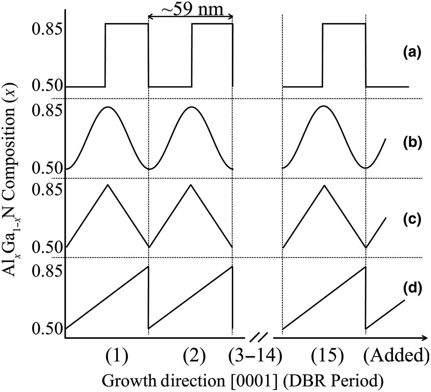
The measured (red) and modeled (dashed blue) reflectivity spectra for the square, sinusoidal, triangular, and sawtooth DBRs.[ Reference Brummer, Nothern, Nikiforov and Moustakas 145 ]

Acknowledgments
I would like to thank all of my students whose work on AlGaN alloys and devices have been reviewed in this article. Thanks are also due to a number of colleagues at Boston University and other Institutes with whom I collaborated on the topics discussed in this article (Professors Soumendra Basu, Enrico Bellotti, Luca Dal Negro, Clemens Heske, Theodore Karakostas, Philomela Komninou, Karl Ludwig, Roberto Paiella, Kevin Smith, and David Smith; Drs Emanuel Dimakis, Alexey Nikiforov, and Emanuele Pecora). This work was supported in part by the NSF Division of Electrical, Communications, and Cyber Systems standard Grant No.1408364, overseen by Drs. Mahmoud Fallahi and John Zavada.


 Open access