


Introduction
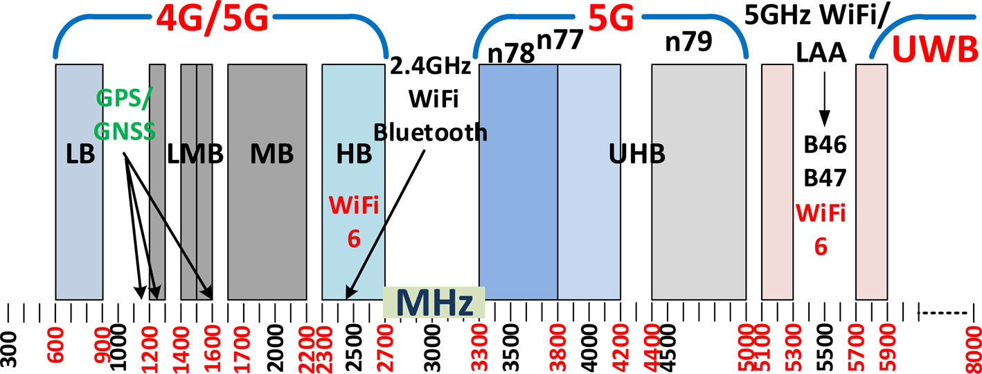
The continuous need for high data rate in smartphones and mobile devices and the arrival of new applications is driving the transition from 3G/4G long-term evolution (LTE) and adoption of 5G LTE [Reference Chen, Gaal, Montojo and Zisimopoulos1]. To provide the increased data rate 5G is using sub-6 GHz bands [Reference Pehlke, Brunel, Walsh and Kovacic2–5] and millimeter-wave (mmWave) spectrum [Reference Rappaport, Sun, Mayzus, Zhao, Azar, Wang, Wong, Schulz, Samimi and Cutierrez6]. 5G together with other RF technologies such as Bluetooth, WiFi6 [7], licensed assisted access (LAA), enhanced licensed assisted access (eLAA), and ultra-wideband (UWB) and sensing and computation techniques will enable new applications; for example, remote medicine (eHealth), vehicle-to-vehicle communications (V2X), factory automation, self-driving vehicles, and internet of things (IoT). 5G is a revolutionary technology step that will make possible new applications which require high data rate, ultra-reliable and low latency communications (URLLC) [Reference Le, Salim and Kaltenberger8, Reference Esswie and Pedersen9], and massive connectivity to a computing cloud. With the adoption of 5G the smartphone device will become a fast and reliable conduit between smart sensors, actuators, and cloud computing. 5G smartphones need to carry over the legacy voice (2G/3G) and need to integrate sub-6 GHz bands as well as add WiFi6 and 4 × 4 multiple input, multiple output (MIMO), to provide high data rate and seamless transition to 5G. These additions and the requirement for one/two stock keeping units (SKUs), add a lot of pressure to keep a balance between increased functionality and additional cost and size associated. The 5G new radio (NR) requirements are specified for extended bands compared with 3G/4G as presented in Fig. 1 for under 6 GHz spectrum.
4G/5G and WiFi6 spectrum – FR1.
The new 5G bands provide more bandwidth (BW) but also come with more technical challenges regarding the integration and RF interferences. Recently the 3rd Generation Partnership Project (3GPP) standard committee extended the 5G millimeter-wave bands up to 71 GHz [10] with up to 2 GHz modulation BW and downlink (DL) carrier aggregation (CA) as presented in Table 1.
5G millimeter-wave spectrum – FR2
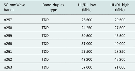
With the introduction of the mmWave bands for 5G, the frequency bands are divided into two frequency ranges:
• Frequency range 1 (FR1) includes all existing and new bands and corresponds to 450 MHz–6 GHz; sub-6 GHz bands. These bands have been used for initial 5G deployment and carry the most 5G traffic right now.
• Frequency range 2 (FR2) includes new bands and corresponds to mmWave bands 24.25–71 GHz. Just several smartphone models carry mmWave modules due to size, power consumption, and extra cost.
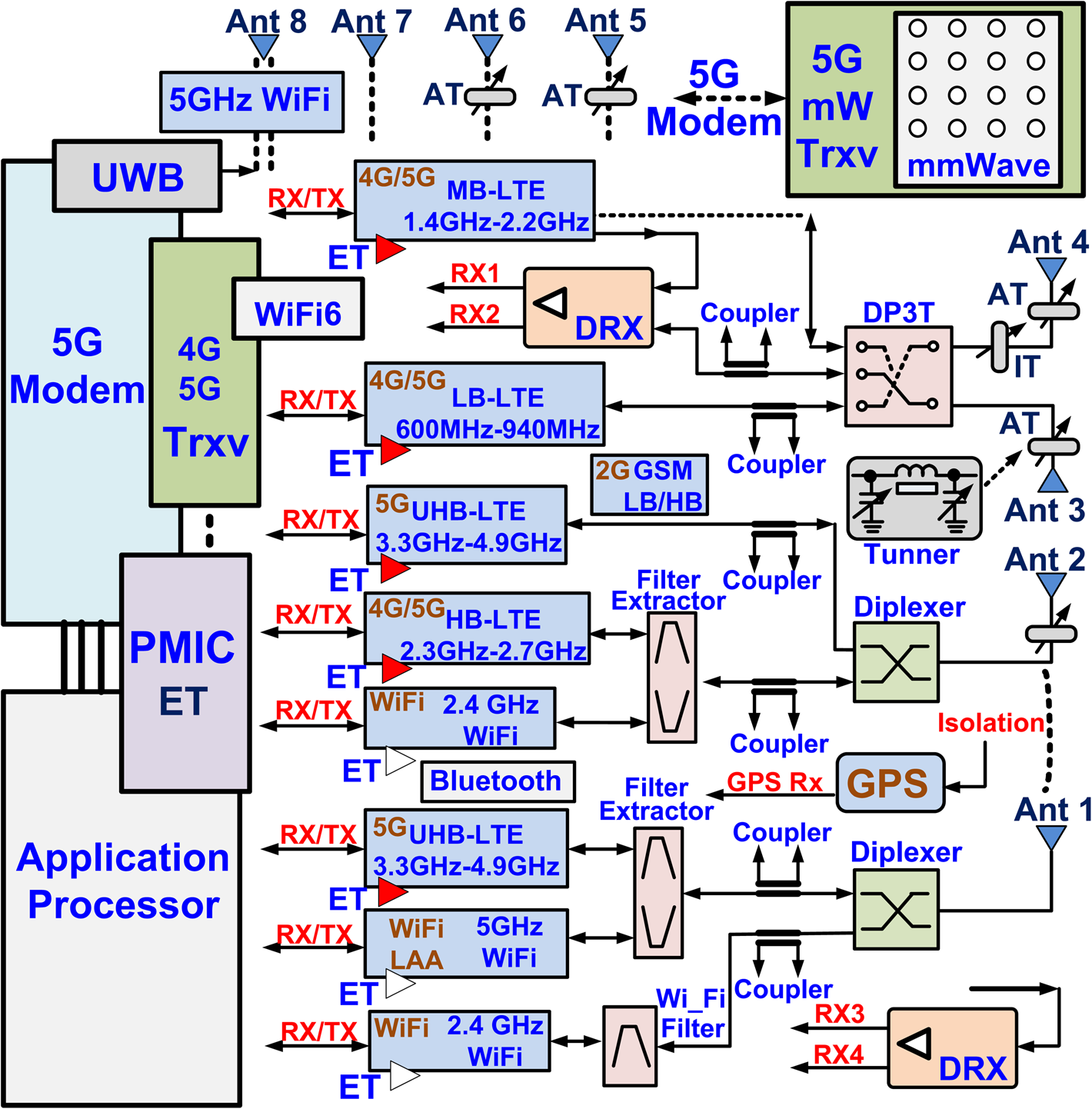
A typical RF front-end module (RFFE) [Reference Chen, Gaal, Montojo and Zisimopoulos1–5] for 5G mobile devices (Fig. 2) has 6–8 antennas for under 6 GHz space (5G, WiFi) and an 8/16 channel mmWave module.
5G RF front-end structure for smartphones.
The main goals for 5G NR are to achieve low latency and date rates of 1 GB/s. The capacity of a wireless system is determined by the Shannon's formula as:

To achieve higher capacity these are the techniques which are incorporated in 5G:
• Increase channel bandwidth Bw; e.g. 100 MHz LTE.
• Increase spatial multiplexing level k through MIMO.
• Increase the transmit power (Tx) and Sk; as 26 dBm for high power user equipment (HPUE) in 5G.
• Decrease noise Nx and improve receiver (Rx) sensitivity.
• Reduce in-band interference Ik on link k, especially in multiple uplink (UL) Tx such as CA and MIMO.
• Higher order quadrature modulation (QAM) such as 256 QAM for UL; this requires an error vector magnitude (EVM) lower than 3/5% [Reference Pehlke, Brunel, Walsh and Kovacic2, Reference Pehlke3].
• Increase signal Sk through use of envelope tracking (ET) – en factor.
Low latency is required for real-time applications such as self-driving and autonomous cars, telemedicine, factory automation as well as smart machines communicating in real time. There are significant challenges for 5G RFFE such as:
• 5G mobile devices need 6–8 antennas which must be reached from different 4G/5G LTE radios which must coexist with multiple WiFi6 radios, Bluetooth, GPS, and UWB.
• 5G introduced dedicated bands for sub-6 GHz such as n77/n78 (3.3–3.4 GHz), n79 (4.4–4.5 GHz), and eLAA bands B46 and B47 (5.15–5.92 GHz) [Reference Chen, Gaal, Montojo and Zisimopoulos1, 5].
• Wider channel BW up to 100 MHz for FR1.
• Very wide channel BW up to 2 GHz for FR2 [10].
• 5G NR introduces high peak to average power ratio (PAPR) waveforms; PAPR is 10.5 dB for UL and 64/256 QAM modulation BW [Reference Chen, Gaal, Montojo and Zisimopoulos1].
• The need for dual-sim operation for voice under second generation of cellular networks, based on the Global System for Mobile Communication (2G GSM) and data (3G/4G/5G) increases the linearity requirements for multiple Tx/Rx path operating at the same time.
• Intra-coexistence with the actual 3G/4G bands in 5G frequency division duplexing (FDD) and time division duplex (TDD) re-farmed bands [Reference Chen, Gaal, Montojo and Zisimopoulos1, Reference Pehlke, Brunel, Walsh and Kovacic2]. 5G NR, as name suggests, provides more data capacity, and allows subscribers to use the 5G networks. There are also existing 3G and 4G radios and therefore we must have design considerations to avoid interferences and to provide handover mechanism so that the user equipment (UE) can access any service available based on their device capabilities and subscription. 5G non-standalone (NSA) provides capacity where 5G NR sites can connect to existing 4G Core (4GC). 5G standalone (SA) provides capacity where 5G NR sites can connect only to 5G Core (5GC). From RF circuit perspective the challenges are reflected in higher requirements for linearity and noise performance.
• Maintain at least −38 dBc adjacent channel power ratio (ACPR) or adjacent channel leakage ratio (ACLR); both terms are used interchangeably.
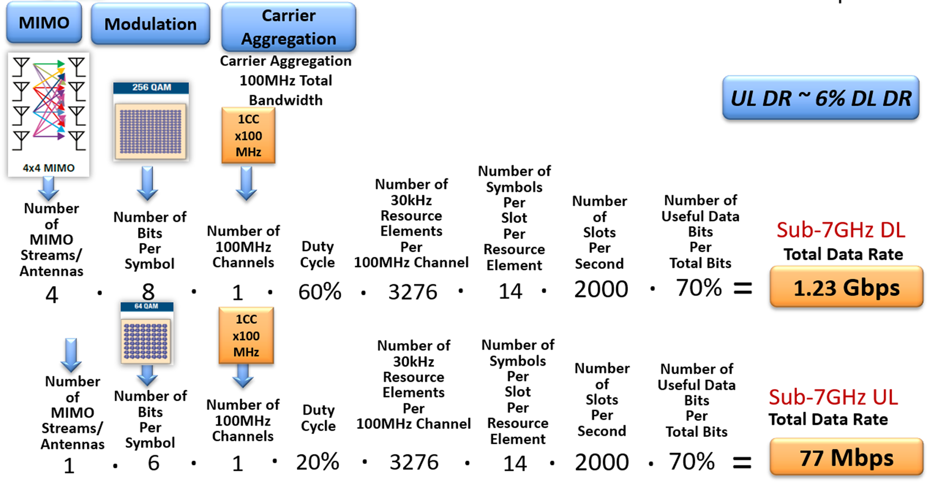
Low latency is the prerequisite for real-time applications such as self-driving and autonomous cars as well as smart machines communicating in real time. Reliable high data rate and low latency are important in connecting smart devices in 5G. With the transition from 4G to 5G one of the key enablers is the subcarrier spacing (SS) which is no longer fixed at 15 kHz and is flexible to cover different latency requirements and frequency ranges, SS is from 15 to 60 kHz for lower frequency bands and from 60 to 240 kHz for higher frequency bands. This will allow the use of short mini slots which will be useful for low latency applications as well as LTE 5G NR coexistence and beamforming. The theoretical data rate (DR) [Reference Pehlke, Brunel, Walsh and Kovacic2] is given by the formula:

where ns represents the number of bits per symbol (8 bits for 256 QAM), m represents the number of MIMO data streams, ncc represents number of component carriers for CA, nsb represents number of sub-carriers, rb represents number of resource blocks (RBs), nss represents number symbols per slot, nsl represents number of slots, ovh (in percentage) is the overhead required for control and coding, and tddov represents TDD duty cycle. Using this formula for 5 × 20 MHz CA streams, 4 × 4 MIMO, and 256 QAM, the DR (Fig. 3) is

5G downlink/uplink data rate.
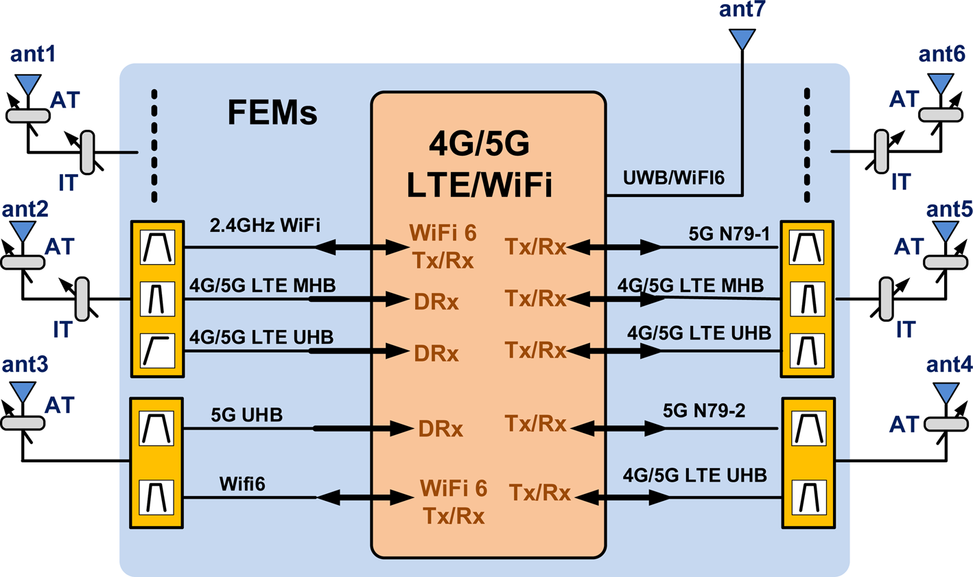
This DL data rate can be obtained using a 4 × 4 MIMO structure with the new 5G mid-high (MHB) bands/ultra-high (UHB) bands (n41, n77, n78, and n79). These bands can accommodate 100 MHz channel modulation BW and 64/256 QAM as presented in Fig. 4. Data speeds of 2.5 GB/s have been demonstrated recently using multiple carriers in FDD and TDD bands [11].
UWB/WiFi6 and 5G MHB/UHB MIMO LTE structure.
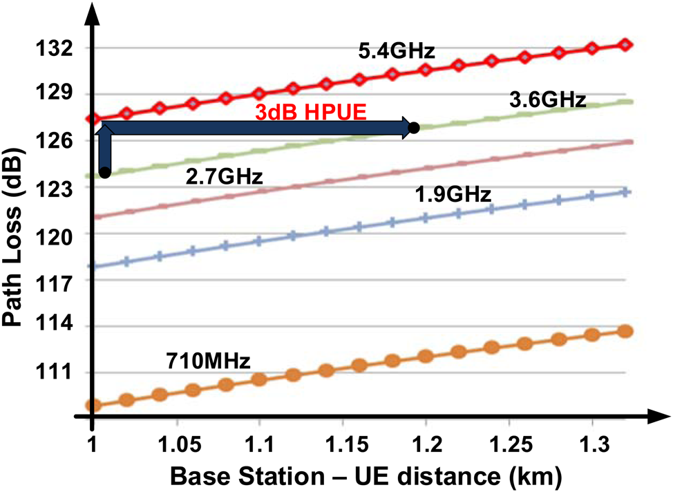
For the majority of smartphone use, the DL is asymmetric compared with UL, but to accommodate a high DL (1 Gbps) as in 5G, assuming 7–10% UL rate for acknowledge/sync signals, 5G needs UL speeds around 100 Mb/s. Due to increases in the use of higher 5G carrier frequencies for 5G such as bands n41, n42, n77, n78, and n79 and higher path loss for these frequencies, 5G has adopted HPUE which increases the RF power delivered at the antenna to 26 versus 23 dBm for 3/4G. This will allow 19% increase in cell coverage radius (42% increase in the base-station coverage area) as shown in Fig. 5.
Path loss for 3GPP cellular frequencies.
All these requirements for 5G determine that more than one Tx in UL together with several Rx in DL as well as multiple radios for WiFi/WiFi6 (2.4/5 GHz), Bluetooth (2.4 GHz), GPS (1.17/1.5 GHz), UWB (6–8 GHz), and smart narrow field communications (13.56 kHz) might be active. All these radios will create RF interferences through conductive and radiated paths. Intermodulation products are determined by all the RF Tx as well as all the other digital clock-related activity in a front-end module (FEM) such as charge pumps, digital mobile industry interface (MIPI) serial parallel interface (SPI) clocks, etc. One of the main design challenges for 5G FEM is how to manage all these RF interferences. Also due to different Rx/Tx configurations between DL and UL and due to high power Tx capabilities for base-stations (40 dBm), the 4G/5G RF UL transmission is the weak link. This becomes more an issue for higher BW and the new 5G MHB/UHB bands.
There are two basic deployment scenarios for 4G transition to 5G networks: 5G SA deployment and NSA deployment. For NSA deployment the UE supports dual connectivity (DC) for 4G LTE and 5G NR. DC will combine the coverage advantage of existing 4G LTE networks with the higher DR throughput and latency advantages of 5G NR. NSA enables 5G NR in smartphones with a smooth evolution from 4G and will be the key to mmWave mobility. Sub-6 GHz anchor will be needed for roaming and handovers as shown in Fig. 6. This anchor band is usually a low band (LB) (450–900 MHz) FDD band due to lower propagation loss [12]. The path loss (PL) from a 15 m height baseband antenna to UE [Reference Chen, Gaal, Montojo and Zisimopoulos1, 12] is determined by

where R is distance and f frequency of operation. PL is dependent on 1/R 4, and for different propagation scenarios for outdoor–indoor, the loss is dependent on 1/f 3.
Cellular structure for 4G/5G with dual connectivity (DC).
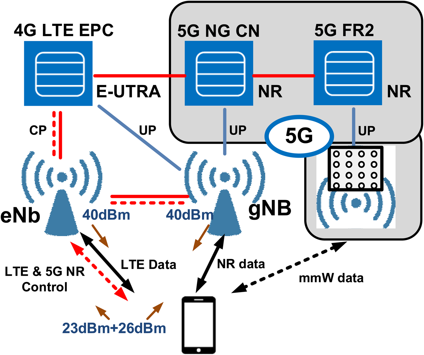
The DC framework allows FR2 network procedures for beam management that are faster than the SA handover for FR2. Especially for FR2, each UE directionally broadcasts a sounding reference signal (SRS) that continuously sweeps the angular space. Each 5G FR2 cell monitors the strength of the received SRS, building a table based on the channel quality of each receiving direction. The optimal FR2 cell and beam configuration are selected for each UE considering the absolute maximum signal-to-noise plus interference ratio. Using FDD bands for FR2 handover will reduce the signaling and calibration time. For FDD there is no guard time between Tx and Rx which limits the capacity and there is no discontinuous transmission required for UL and DL. Also, the base-stations need to be synchronized with respect to the UL and DL transmission times. If neighboring cells use different UL and DL assignments and share the same channel, then interference may occur between cells. The best latency in this process is obtained using LB FDD bands for DC [Reference Esswie and Pedersen9, 11].
5G front-end module architectures
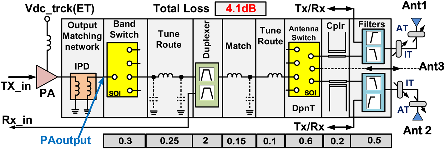
The smartphone market is very dynamic and the move to 5G requires coverage for more than 50 LTE bands from 500 MHz to 6 GHz [Reference Balteanu, Serge Drogi, Modi, Choi, Khesbak and Agarwal13]. These bands cover the entire world with very few mobile SKUs. A lot of research has been done for single die power amplifier (PA) in different technologies such as silicon germanium (SiGe), complementary metal-oxide semiconductor (CMOS), and silicon on insulator (SOI) [Reference Lie, Tsay, Hall, Nukala and Lopez14] but still gallium arsenide (GaAs) is the technology mainly used. With the band proliferation and the transition to 5G the weight in terms of cost and size is determined by the number and type of acoustic filters, such as surface acoustic wave (SAW) and bulk acoustic wave (BAW). The acoustic filters are placed with other components such as PAs, SOI switches, and low noise amplifiers (LNAs) into an FEM with acoustic duplexers/filters (FEMiD). With the increase of the number of antennas and the requirements such as each antenna to be reached by multiple PAs and FEMs, the RF path loss to the antennas, on the mobile device, becomes higher for 5G as presented in Fig. 7. The RF loss can be 4–5 dB, and this RF loss is higher than the typical loss for 3G/4G (3 dB). Unfortunately, this RF loss must be compensated with higher RF power delivered by the PA and increased SOI RF switch size to maintain the linearity.
5G RF path loss from PA output to the antenna output.
Sub 3 GHz bands provide primary LTE cellular coverage, and the new 5G bands provide the increased capacity using MIMO and CA. The typical FEM structure is presented in Fig. 8.
LTE 4G/5G RF front-end module structure.
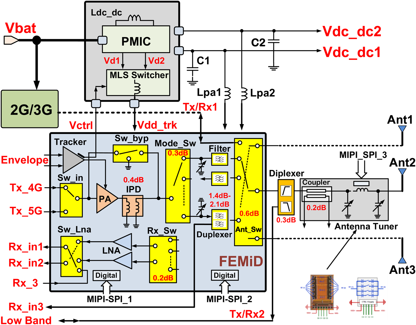
The legacy 2G/3G module is directly connected to the battery but the 4G/5G modules are connected through a power management integrated circuit used also for ET [Reference Paek, Kim, Bang, Baek, Choi, Nomiyama, Han, Choo, Youn, Park, Lee, Kim, Lee, Cho and Kang15]. The TDD FEM can use also the LNAs on the same module; due to isolation this is not a solution for FDD systems that have both UL and DL operating at the same time. This is one aspect of the FEM architecture which must be considered from the beginning together with other mitigations due to multiple intermodulation products for multiple RF transmitters and receivers operating at the same time. Intermodulation products are determined by all the RF Tx paths, including WiFi [Reference Maldonado, Karstensen, Pocovi, Esswie, Rosa, Alanen, Kasslin and Kolding16], and all other clock-related activity as well (charge pumps, MIPI SPI clocks, etc.). There are few types of interference due to simultaneous UL and DL over different bands in CA configurations which will degrade the Rx sensitivity (desense):
• Interference from sub-harmonic mixing for CA case when the higher UL frequency signal is a multiple of the lower frequency (Band 7 and Band 27/CA case) and desense the LB Rx.
• Interference from the harmonic of lower frequency UL signals to the higher frequency DL when the harmonic of UL lands into UL Rx frequency band. For example, when a UE is transmitting on Band 3 4G/LTE and receiving on 5G NR bands n77/n78. Second harmonic of Band 3 will land into 5G NR Rx for bands n77/n78. Another CA case for desense is when 3rd harmonic (H3) from LB lands in RX high band (HB) as presented in Fig. 9.
• Intermodulation distortion (IMD) products between different Tx frequencies and/or MIPI SPI and charge pump clock frequencies.
FDD FEM low band to high band desense in smartphones due to third harmonic.
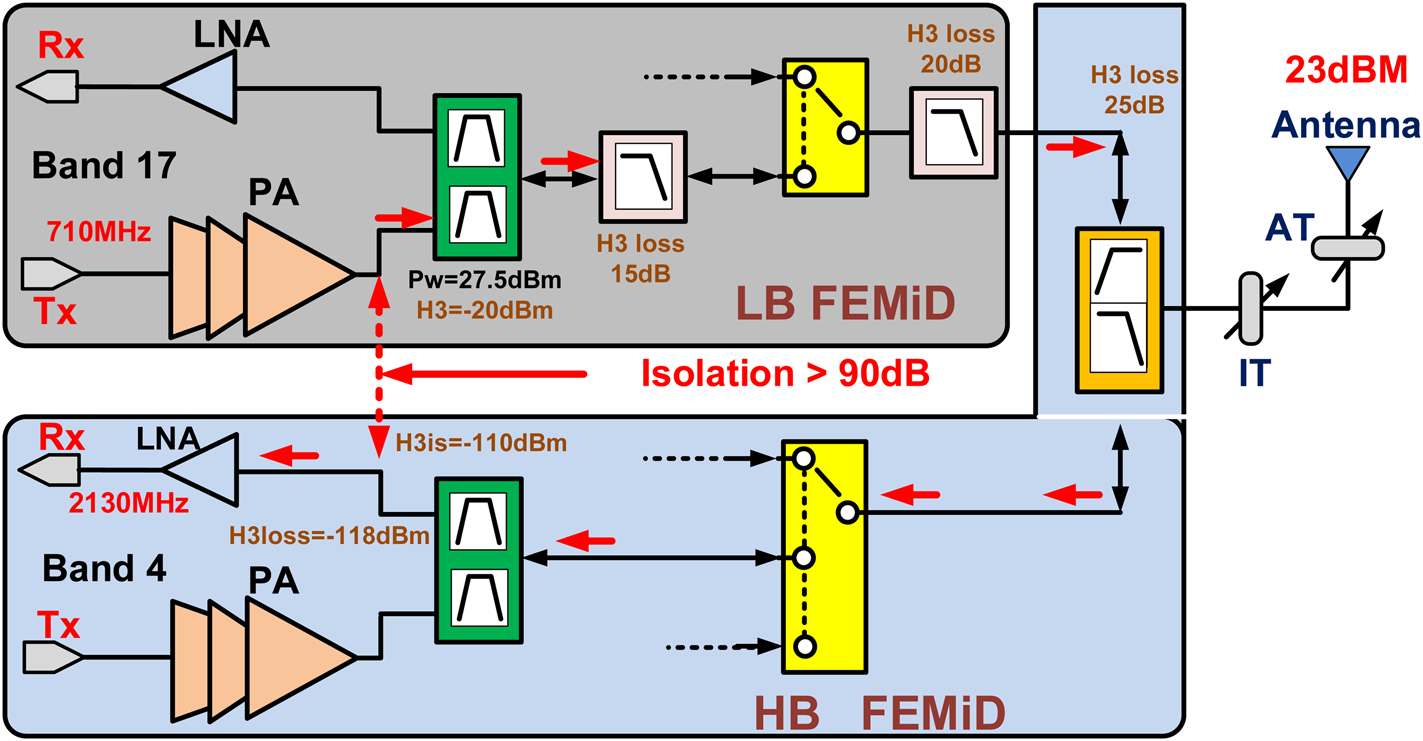
To avoid any desense due to third harmonic, at least 90 dB isolation is required; this requires FEMiD shielding and special routing on the smartphone board.
Power amplifier
The RF PA is one of the core components for the FEM due to efficiency and linearity requirements, especially with the transition to 5G. With the adoption of 256 QAM for 5G UL the PA linearity expressed through EVM is started to be challenging to be met (<3.5%), although 5G allows 4–6 dB maximum power reduction (MPR) for 64/256 QAM 5G cyclic prefix–orthogonal frequency division (CP-OFDM) signals. Several techniques have been used to meet the efficiency and linearity requirements, the most extensively used and researched being Doherty and ET PAs [Reference Grebennikov17–Reference Kahn19]. The adoption of both techniques has been possible by advances in digital signal processing and technology scaling such as 7/3 nm FinFET. Doherty techniques provide high efficiency but have limitation in terms of broadband operation, operation in back-off mode, and load mismatch [Reference Zenteno, Isaksson and Händel20].
In mobile applications, such as smartphones, ET is used with a broadband PA with class E output match for low (LB), middle (MB), high (HB), and ultra-high (UHB) bands. The class E PA (Fig. 10) with parallel components has been introduced in [Reference Grebennikov and Jaeger21]. The optimum series feed inductance L and parallel capacitance C [Reference Grebennikov17, Reference Grebennikov and Jaeger21] can be obtained by the formulas:

Power amplifier class E output match.
Lo and Co provide the series resonance, and for different bands, the structure might have 2Fo and 3Fo traps. As presented in [Reference Kim, Son, Kim, Jang, Oh and Park22, Reference Dinc, Kalia, Akhtar, Haroun, Cook and Sankaran23] this structure can be used with a differential transformer/balun. In [Reference Balteanu, Drogi, Hardik, Choi, Khesbak and Agarwal24] a HPUE PA with an ET has been presented. Using the same approach, a high resistivity CMOS 0.18 μm PA with a push–pull class E output stage and integrated fast error amplifier is presented in Fig. 11.
LTE 4G/5G push–pull power amplifier.
The PA operates in class E [Reference Grebennikov and Jaeger21] and can use two or more push–pull structures to provide HPUE power capability (26 dBm) at the antenna for high 5G bands and operates with good efficiency at lower RF power levels. At lower power levels, few PA cores can be turned off. The ET structure is using an AC combiner which doesn't require a DC tracking loop [Reference Grebennikov17]. This is well suited for high modulation BW where the large AC coupling capacitor and the DC tracking loop will slow down the ET operation. One of the issues using ET [Reference Lie, Tsay, Hall, Nukala and Lopez14, Reference Grebennikov17] is the noise generated in the adjacent Tx channels especially for multiple Tx transmitters operating at the same time. To accommodate different Tx power levels and multiple Tx operating simultaneously, the ET can be operated in two modes:
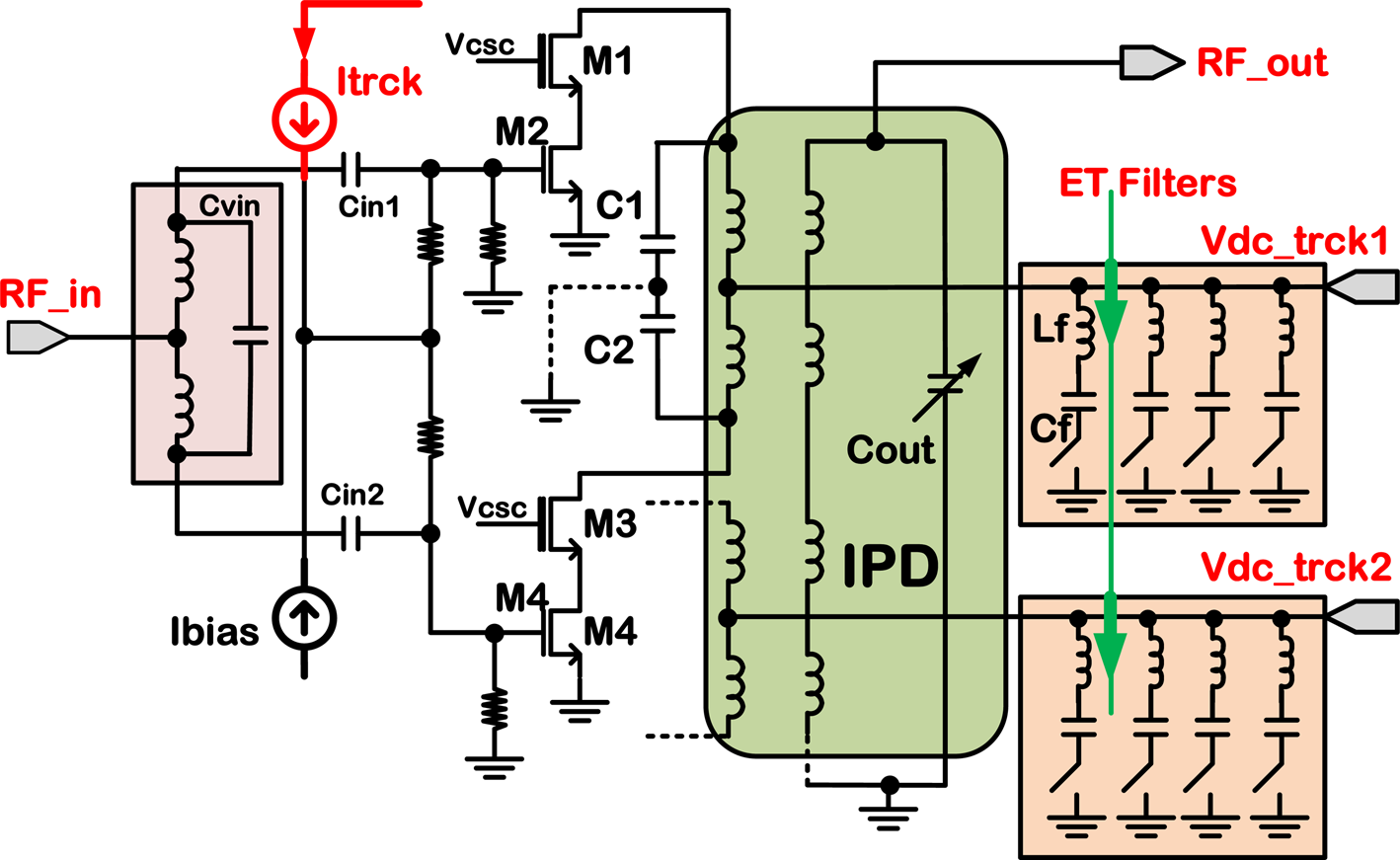
(1) For lower modulation BW with less LTE RBs, the ET is done through the PA current bias (Itrck) as presented in Fig. 11 and the error amplifier is turned off.
(2) For higher RBs and multiple PA operating at the same time, the ET fast amplifier is turned on. Based on the signal modulation BW, different low frequency filters are selected on the Vdc_trck ports. This helps with the RF noise due to low frequency up conversion noise.
(3) Both Itrck and ET fast amplifiers are activated; assuming the envelope delays are well controlled.
Bias control for polar loop transmitters was introduced and described in [Reference Sowlati, Rozenblit, Pullela, Damgaard, McCarthy, Koh, Ripley, Balteanu and Gheorghe25] and can be extended to ET systems. For high modulation BW, such as in 3G/4G/5G, the polar approach is limited by the delay alignment for AM and PM paths. ET system is a hybrid approach between polar and linear modulation, where the delay alignment is critical but not as critical such as in polar systems. Assuming the delay is calibrated and manageable, Fig. 12 presents the static PA and ET operation under different bias (ET and PA gate bias) and therefore load line (Rload) conditions. Under ET operation the PA operates in back off mode, in class AB, B and A based on instantaneous RF power. When Itrck current is used and controlled, based on the instantaneous RF power the dynamic operating point is changing from load line 1 to load line 2. The operations in zones 3 and 4 are controlled by the Vdc_trck 1 and 2 voltages applied by the ET system based on a look-up table [Reference Grebennikov17]. Itrck can be generated using a similar look-up table, but this requires modem/transceiver resources. For the practical implementation Itrk is generated from Vdc_trck.
Power amplifier and ET operation.

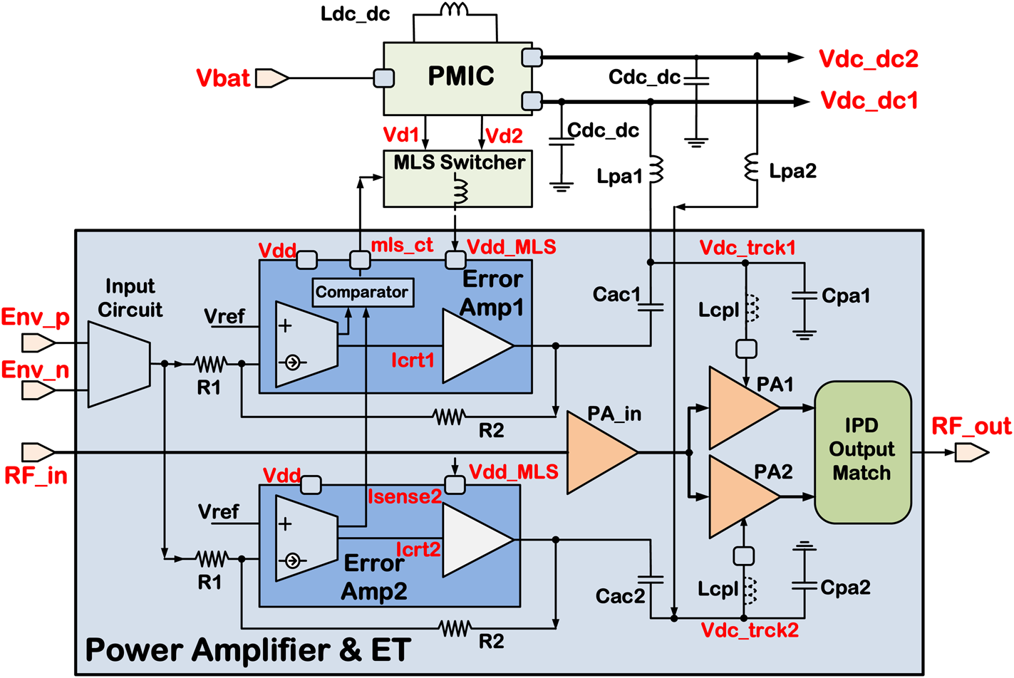
For HPUE, which is a requirement for mid-high 5G bands, two identical DC voltages (Vdc_dc1 and Vdc_dc2) are provided to the ET combiners which are located on the same FEMiD as presented in Fig. 13. This structure allows to achieve higher power at the PA output and accommodate the losses due to RF switches and acoustic filters. These losses are higher for 5G due to multiple antennas routing and higher linearity requirements for SOI RF switches.
5G power amplifier and ET.
The PA bias (Fig. 14) needs to provide the required current for the PA with low impedance to cancel the second-order input intercept point (IIP2) terms which might be upconverted and degrades the EVM and the ACPR/ACLR. The low impedance bias mitigates the current imbalances which produce ACPR/EVM degradation.
Differential PA bias structure.

Also, the feedback bias amplifier (Fig. 15) must provide enough BW for the bias current. Due to these considerations a simple current feedback structure with source follower is used. To decrease the output impedance for quite large BW, a low Rs impedance is required but this increases the current consumption. From this perspective a programmable Rs is used.
Differential PA bias structure detail.

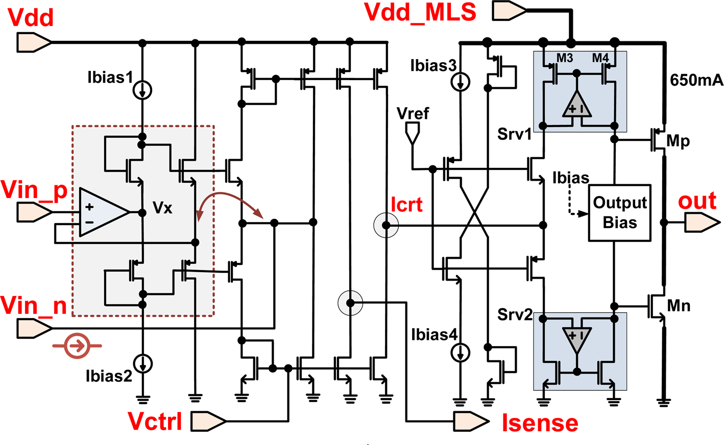
The error amplifier which is part of ET is a current feedback amplifier with two stages and is presented in Fig. 16. The second stage is biased from Vdd_MLS where the voltage is set based on the modulation PAPR and the PA power level. This is determined with a comparator which senses the error amplifier output current through Isense pin. The Vctrl pin is used to compensate the current offset with a low-frequency feedback loop [Reference Drogi, Balteanu and Pehlke26].
Current feedback error amplifier schematic.
When the PA is operated in the ET mode the voltage supply applied to the PA Vdd = Vdc_trck is following the envelope signal (instantaneous power level). The peak voltage applied is determined by the maximum power which must be delivered under ET for different peak to average power ratio (PAPR) waveforms [Reference Grebennikov17]:

With the adoption of 5G there is an increase to 10.5 dB of the PAPR for all the waveforms. This determines the requirements for increased slew rate for the error amplifier and this is the main reason for using a current feedback amplifier.
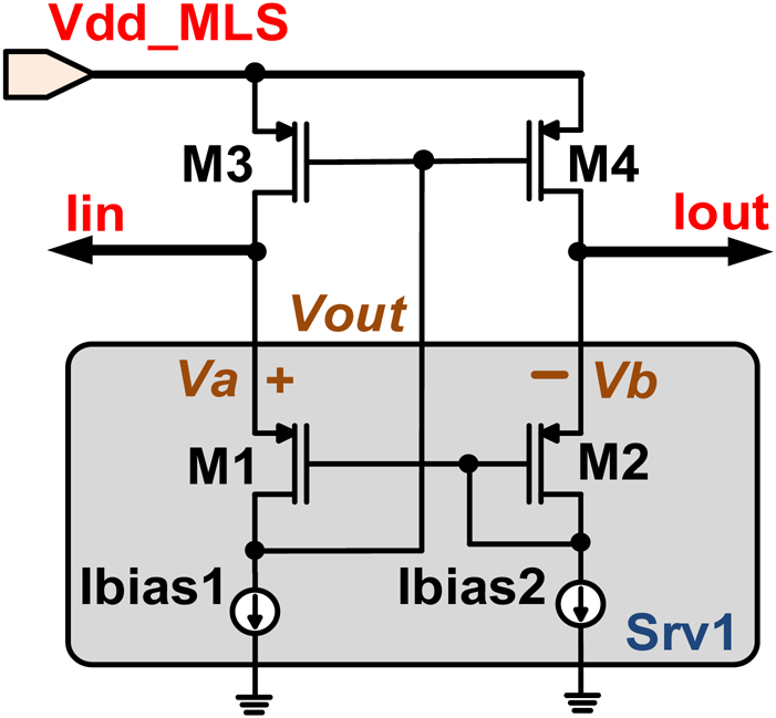
To maintain a constant current and avoid any peaking and instability the error amplifier uses two current mode servo amplifiers Srv1 and Srv2 in the final stage as presented in Fig. 17. Using a current mode structure, the servo amplifiers provide a high operation BW and low propagation delay.
Servo amplifier detail.
RF FEM SOI switches for 5G
The RF switches are integrated as separate dies to increase isolation and are fabricated in 0.18 μm SOI technology. The SOI switch structure is presented in Fig. 18.
FEM RF SOI switch schematic.
For 5G FEMs, due to power increase for HPUE and increased PAPR for 5G NR waveforms, the number of series in FETs must be increased and determined by the formula:

where VDS_peak is the peak NFET drain source voltage. For off state the peak RF voltage across FET drain-source for each transistor assuming equal voltage division is:

where Vth is the threshold FET voltage.
As presented in [Reference Zhu, Klimashov, Roy, Blin, Whitefield and Bartle27] the maximum breakdown voltage is determined by:
The insertion loss (IL) and the input intercept point (IIP3) [Reference Zhu, Klimashov, Roy, Blin, Whitefield and Bartle27, Reference Balteanu, Zhu and DiCarlo28] for a series-shunt switch are defined by the equations:


where Ron is the on-state channel resistance of the switch and Vpos is the positive voltage

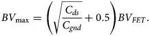
Unfortunately for 5G the RF path losses are higher and the power requirements at the antenna are increased and therefore the switch performance requirements are more challenging. With two or more RF transmitters operating at the same time there are higher linearity requirements for antenna SOI switches as well as antenna tuning elements. For example, assuming sensitivity of a typical LTE 5 MHz (25RBs) as −101.5 dBm and 4.5 dB margin, the linearity requirement IIP3 to avoid jamming assuming Tx1 and Tx2 (Fig. 19) is given by:

Cellular intermodulation distortions and cellular/WiFi desense.
Tx2 assumes 26 dBm which is required by the 3GPP with release #17 [10].
Assuming an external blocker at −30 dBm and a Tx2 UL signal at 23 dBm the switch linearity IIP2 is given by:

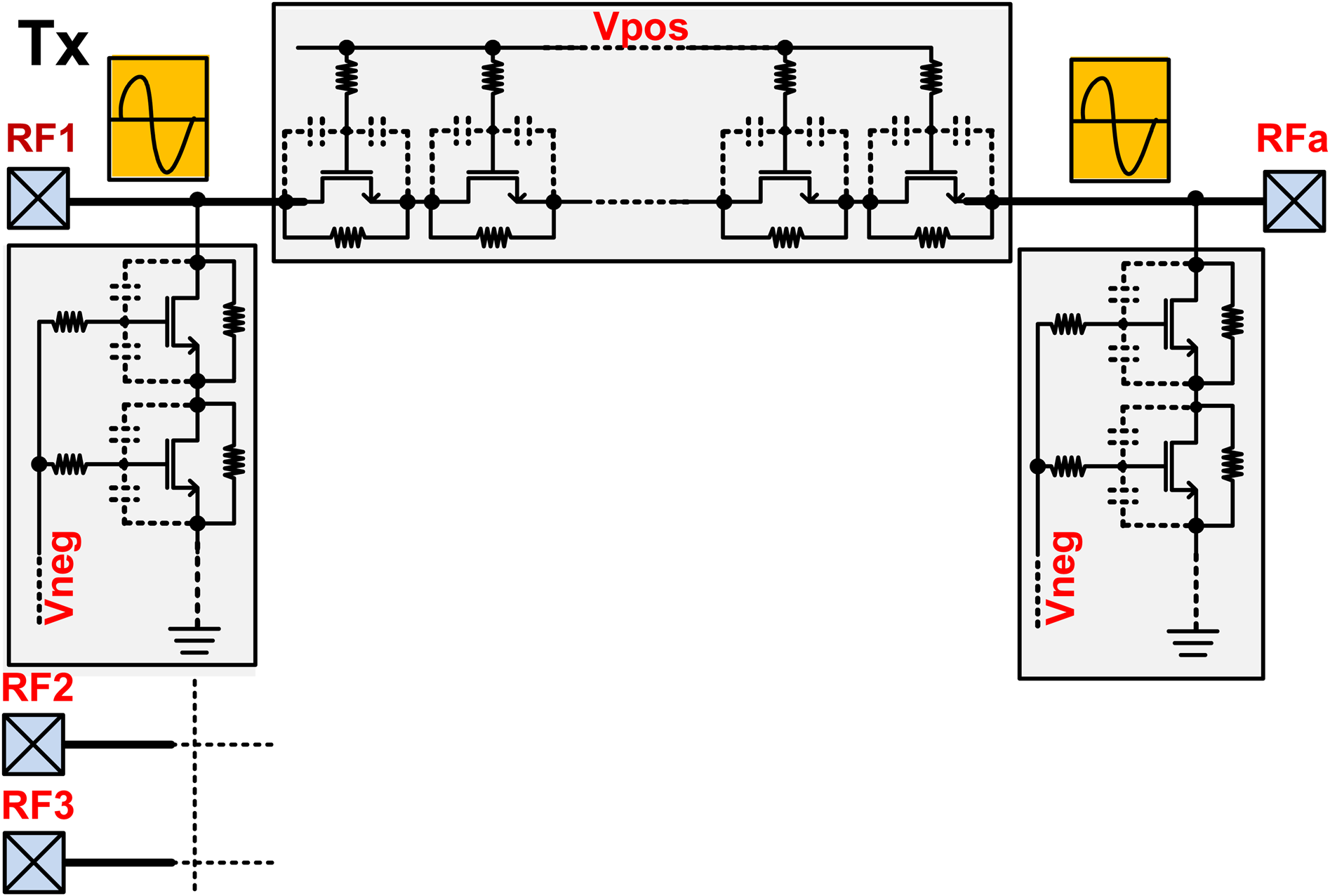
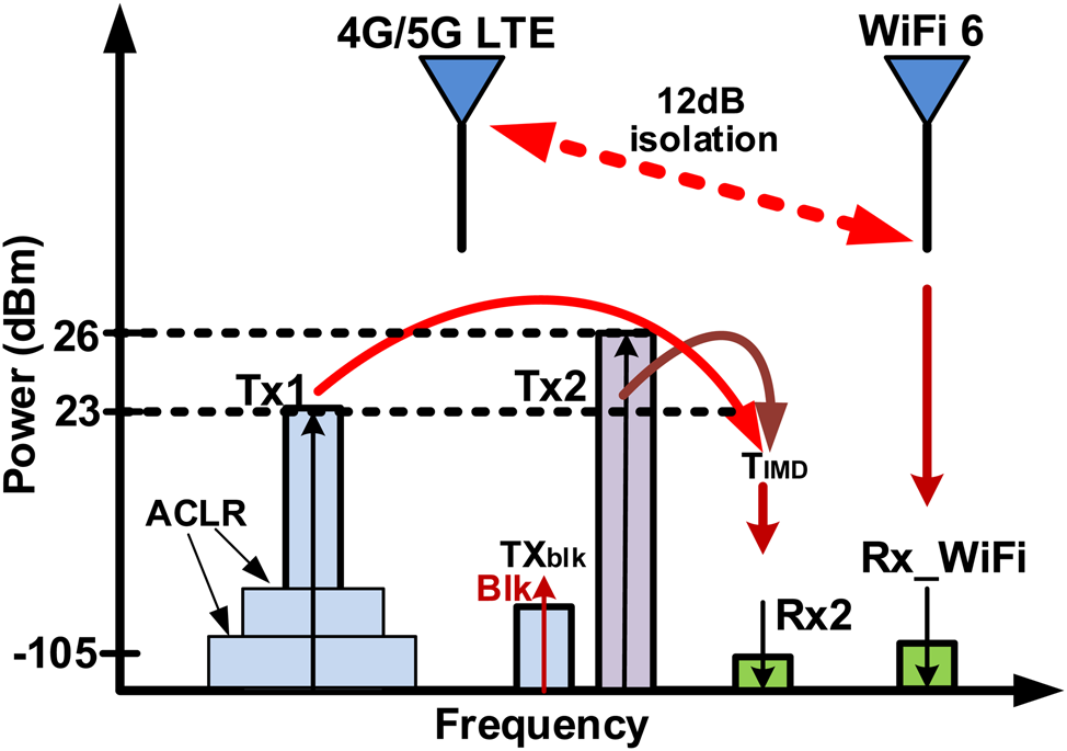
To speed up the RF SOI switch transition, for a time response less than 1 μs (as required in 5G for low latency), a seven-stage ring oscillator with an activated clock doubler (for RF switching) is used. In order to generate Vpos and Vneg for the switch control [Reference Balteanu, Zhu and DiCarlo28], a negative/positive charge pump is used and presented in Fig. 20. This schematic has a ring oscillator structure with seven stages. For normal operation, the charge pump clock frequency is reduced using several dividers. Low clock frequency reduces the clock feedthrough into the RF PA in the Tx chain as well as Rx LNAs. For Tx applications there is a limit of the clock frequency reduction, due to effective reduction for Vneg and therefore a reduction for maximum RF power handling as expressed by equations (7) and (8).
RF SOI switch positive/negative voltage generation with clock doubler.
RF 4G/5G acoustic filters
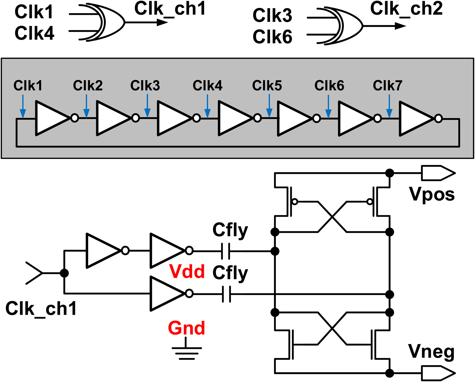
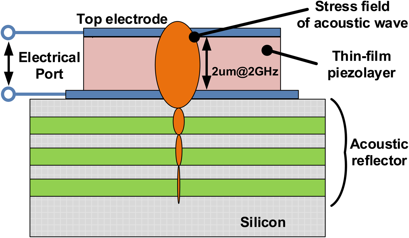
The transition from 3G/4G to 5G, with requirements for different RF transmitters’ coexistence, drives the use of several acoustic filters. For lower frequencies, up to 2 GHz, the filter requirements have been handled using SAW filters (Fig. 21). With the evolution to 5G and more HB and UHB FEMs, there is a high demand for BAW filters (Fig. 22). SAW filters can be used up to 2 GHz and must be temperature compensated (TC-SAW) to operate across a wide temperature range and to accommodate reduced guard bands, which is the case for 5G LB FDD filters.
SAW acoustic filter structure.
BAW acoustic filter structure.
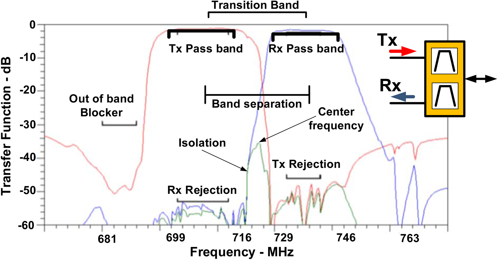
BAW acoustic filters present quality factors of 2000 and 3000, which are higher compared with SAW filters, but require more precise steps in fabrication and are more costly. In Fig. 23, the measured TC-SAW acoustic filter characteristic for band n12 with 51–61 dB Tx rejection in Rx band is presented.
TC-SAW acoustic filter response.
With the adoption of 5G for FDD LBs and the use of high modulation BWs, such as 64/256 QAM, the Tx and Rx filter flatness is crucial. There are many efforts in this area to reduce the spurious resonances in band caused by traverse modes [Reference Liu, Liu, Wang and Lam29], which produce different group delays based on the frequency of operation in Tx/Rx bands. The traverse mode suppression improves the ET delay calibration precision and reduces the time of ET calibration due to reduced number of frequency points for calibration.
Implementations and measurements
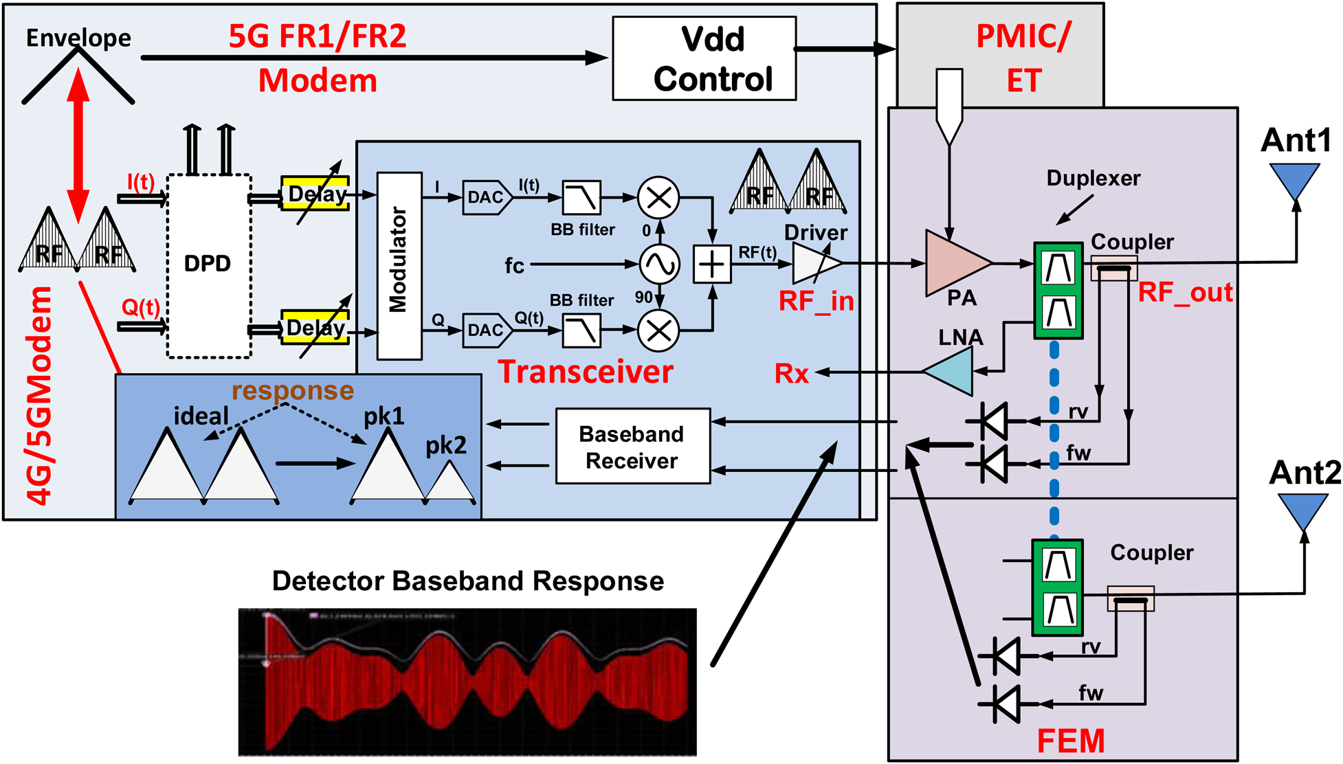
FEMs for smartphones end up into very high-volume products and therefore all the costs and hardware integration tests associated with the functionality must be considered. One of the RF Tx aspects is the calibration. Calibration also requires frequency equalization due to Tx and duplexer response for different modulation BW from 1.4 to 100 MHz. An ET calibration method where a baseband envelope signal is aligned using a triangular low intermediate frequency (IF)-modulated RF signal has been presented in [Reference Balteanu, Zhu and DiCarlo28] and used in current 4G/5G mobile devices. The delay is adjusted until the baseband-received signals have the same peak values. These RF peaks require an observation receiver to be processed. The observation receiver is a prerequisite of actual 4G/5G transceivers but the time for testing and calibration is increased. This contribution introduces a new calibration method where instead of the observation receiver a fast peak/rms detector is used, as presented in Fig. 24.
FEM calibration for RF power and ET delay.
The peak detectors are very precise for PA power measurements (±0.2 dB) and the response BW can be adjusted from 1 GHz to lower frequencies such as 2 MHz. This allows for power measurements considering different modulation BWs and can be extended to mmWave FR2 measurements. Also, by using a baseband envelope signal with several peaks this can be aligned after detection and the ET delay calibrated. For higher modulation BW the ACLR is strongly depended on the delay mismatch as presented in Fig. 25, where the PA is set at lower power levels to avoid ACLR degradation due to heavy non-linearities.
ACLR versus ET delay mismatch.
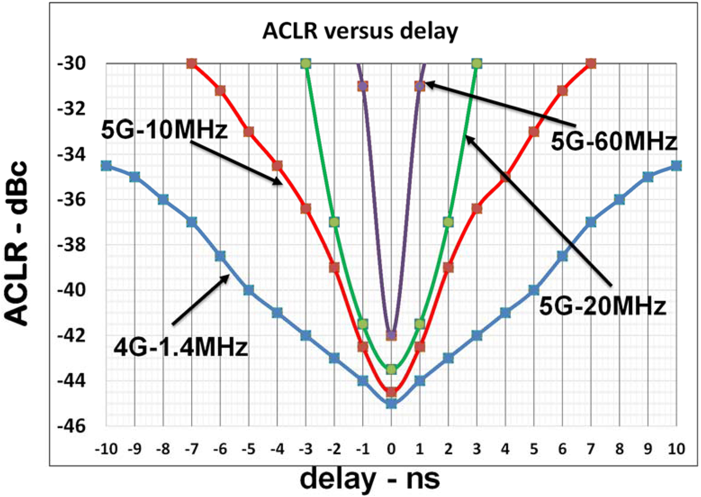
As general rule, for 20 MHz modulation BW the delay should be calibrated below ±0.5 ns to have good efficiency and at least −38 dBc ACLR for high power levels.
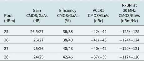
For one implementation, the PA, ET amplifier, and ET control and error amplifiers have been implemented using 0.18 μm CMOS with high resistivity technology with through silicon vias. Together with RF SOI switches and RF acoustic filters, all are integrated on the same substrate in a multi-chip-module. The worldwide transition of smartphones to 5G and the worldwide adoption for billions of people are one of main driving engine behind semiconductor industry. From this perspective the costs associated with the smartphone hardware as well as fabrication and field calibration must be considered. One of the important aspects for 5G Tx and Rx integration is the RF noise and noise measurements in production. The ET filters (Fig. 11) as well as charge pump noise mitigation have been implemented to provide enough margin from the design phase for the FEM noise in Rx band. In this way there is no need to check thoroughly during FEM production. RF noise mitigation is especially challenging for low frequency 5G bands where the duplex space is 30 MHz as in FDD bands n12 (699 MHz–716 MHz-UL/729 MHz–746 MHz-DL) and n13 (777 MHz–787 MHz-UL/746 MHz–756 MHz-DL). The Rx noise figure (NF) will degrade with 0.5 dB for a TX noise level lower than −120 dBm/Hz in Rx band. The FDD acoustic filter has a significant influence on the Rx band noise performance as the typical duplexer isolation between Tx and Rx is between 51 and 61 dB. Assuming the noise floor to be approximatively −174 dBm/Hz, for just 0.1 dB NF degradation, the noise after duplexer needs to be below −184 dBm/Hz. The noise measurements are shown in Fig. 26. For band n12 the measurements show low noise of −124 dBm/Hz at 30 MHz duplex space using an ET low-frequency filter with Lf = 39 nH and Cf = 1 nF (Fig. 10); Pout = 26 dBm. With the new TDD 5G bands [Reference Pehlke3] in the so-called C-band (n77, n78, and n79), there will be more BW available for high data rate but still the low-frequency bands will be used as 4G/5G LTE communication anchors. For example, right now the majority of 5G deployments use primarily 3.5 GHz TDD bands using NSA mode but will transition to SA. Table 2 presents the measurements for LTE 5 MHz, 710 MHz, Band n12 (30 MHz LTE BW), which exhibit very good efficiency for ACLR1 = −38 dBc, without digital predistortion, for 64 QAM. These measurements are done at the PA output. For 5G LBs, the power required at the antenna is 23 dBm and, with 5 dB MPR for 64 QAM CP-OFDM, the PA can be used in a LB FEM.
Rx noise measurements for low-frequency 5G FDD bands – n13 and n12.

CMOS 0.18 μm and GaAs PA and ET measurement results for LTE 10 MHz, 64 QAM, band n12
Similar implementation has been done using a GaAs PA (Fig. 27) with an integrated passive device (IPD) balun. In this case the ET bias and control circuitry is on a separate 0.18 μm CMOS die. The efficiency observed was better for GaAs versus CMOS, with almost 3–4% for the same ACLR and noise levels. For both implementations there is a penalty in terms of size using an IPD balun. At LBs (400–1200 MHz), using a balun helps with the second harmonic suppression for coexistence with other 5G transmitters and mitigates the low breakdown voltage for CMOS devices [Reference Balteanu, Drogi, Hardik, Choi, Khesbak and Agarwal24, Reference Aoki, Kee, Magoon, Aparicio, Bohn, Zachan, Hatcher, McClymont and Hajimiri30]. For size constrained applications, which is the case for 5G smartphones, the use of IPD baluns becomes practical for higher FR1 frequencies, such as n41, n77, n78, and n79 or FR2 mmWave frequencies.
Power amplifier GaAs die for low bands 600–1200 MHz.

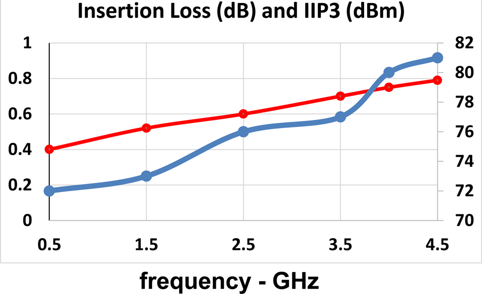
In Fig. 28, the measurements for a DP6T SOI switch used in the FEM are shown. The IIP3 is lower than 89 dBm as derived in equation (14). In this case the RFFE must operate under MPR or be used with different antenna route.
DP6T insertion loss and IIP3 measurements for 50 Ohm load.
Conclusion
Smartphone industry is a very large volume industry where hardware changes and improvements take long time to be tested for functionality and reliability before being deployed. 5G FEM architectures have been presented and a fully integrated 0.18 μm LB FDD CMOS PA and tracker was packaged and tested into FEM together with SOI switches, duplexers, and filters. Same tests have been performed using a GaAs PA. Elements of this architecture with CMOS PA and ET collocated, used for 4G, have been presented initially in 2014. This paper presents FEM circuit improvements for noise reduction and increased linearity through ET. Elements of this architecture with CMOS PA and ET collocated, used for 4G, initially have been demonstrated at the 2014 Mobile World Congress, Barcelona, and have been improved for HPUE and 5G. The next step for 5G deployment, as has been demonstrated at the 2022 Mobile World Congress, Barcelona, is to move toward SA mode using the new 5G CA core architecture using FDD LB bands operating in 700 MHz (n12, n13, n28) along with supplemental DL MB band 1400 MHz (n75) and UHB 3500 MHz (n78). Also, the use of FDD LB for 5G will enable better URLLC services due to lower latency. This will power enhance consumer experience with faster peak speeds and higher throughput and allow for industry growth in areas such as industrial IoT and cloud services.
The novel circuits and calibration methods in this paper will make 5G RFFE integration possible for next generation mobile 5G applications using FR1 and FR2.
Supplementary material
The supplementary material for this article can be found at https://doi.org/10.1017/S1759078722001295.
Conflict of interest
None.
 Florinel Balteanu received the M.S. degree in electrical engineering from Polytechnic Institute, Bucharest, Romania, in 1983, and the Ph.D. degree in electrical engineering from Transylvania University, Brasov, Romania, in 1995. From 1983 to 1992, he was with the Institute of Nuclear Research, Pitesti, Romania, working on electronic instrumentation for nuclear power reactors. In 1993, he joined the Department of Electronics, University of Pitesti, Romania, as an Assistant Professor doing research in analog circuits. From 1992 to 1993, he was a Fulbright Visiting Scholar at the Center for Reliable Computing, Stanford University, Stanford, CA, USA. In 1996, he joined Philsar Semiconductor, Ottawa, ON, Canada, as a Senior ASIC Designer, a company later acquired by Conexant Systems, Inc. (now known as Skyworks Solutions, Inc.). His work has been focused on the design of radio circuits for GPS receivers, Bluetooth transceivers, and GSM/CDMA cellular transceivers. He is presently a Technical Director with Skyworks Solutions Inc., Irvine, CA, USA and is involved in designing circuits for envelope tracking and front-end modules in CMOS and SOI CMOS. He presented short courses and tutorials as an Invited Speaker at IEEE Microwave Theory and Techniques Society (MTT-S) International Microwave Symposium (IMS). European Microwave Week (EuMW), European Solid-State Circuits Conference (ESSCIRC), and Asia-Pacific Microwave Conference (APMC). He holds 84 US patents, with several more pending. He is the author of the chapter “Envelope Tracking Techniques” in the IET book “Radio Frequency and Microwave Power Amplifiers, Vol. 2: Efficiency and Linearity”.


 Open access