


Introduction
The solid-state noise source finds extensive usage in microwave and mm-wave systems, as a precision reference standard for noise-related characterization in both laboratory and industrial equipment. In this context, a widely diffused application of noise sources is found in radiometer systems, since the mm-wave operation enables the observation of harsh scenarios where optical wavelength hardly propagates through the medium. In addition, with respect to the lower microwave range, mm-wave noise observation is consistent with better space resolution arising from higher directivity compact antennas. Other relevant applications are also found in noise-operated radar systems, which are widely employed in meteorological remote sensing, especially for the lower C and X bands [Reference Glushko and Yanovsky1, Reference Chen, Masini, Yang, Milillo, Feng and Lasaponara2].
Focusing on radiometer systems, the employed measurement technique is extremely sensitive to short-term and long-term fluctuations of noise figure and gain parameters through the whole radio frequency (RF) receiving section. For example, the total-power radiometry [Reference Thomsen3], which relies on a single integrated-power measurement and does not use an on-board noise reference, is a non-practical technique when maximum accuracy and resolution are required. This is because the architecture is affected by noticeable measurement uncertainties introduced by the mentioned parameter drifts; so for these reasons, both temperature-calibrated noise sources and feedback-controlled noise measurement systems should be adopted in industrial applications with high accuracy requirements. Solid-state noise sources, based on the physical principle of avalanche breakdown generation in a semiconductor junction, are often employed in these precision use-cases, thanks to their low cost and ease of integration in conventional monolithic microwave integrated circuit (MMIC) technologies, such as Heterojunction Bipolar Transistor (HBT)-based ones [Reference Alimenti, Simoncini, Brozzetti, Maistro and Tiebout4]. The avalanche noise generation process also exhibits power stability over the long-term [Reference Gupta5, Reference Alimenti, Tasselli, Botteron, Farine and Enz6]. A non-negligible advantage, arising from this type of avalanche source, consists of the straightforward control of generated noise power. This requirement is necessary in some practical radiometer architectures, since the noise source acts as switched resistive terminations, placed at different Hot and Cold physical temperatures, cf. Figure 1, thus generating controlled thermal noise power for calibration purposes [Reference Vidyalakshmi and Arunachalam7–Reference Hach9]. The noise power control is also required to dynamically optimize the trade-off between instrument resolution and dynamic range, by varying the calibration noise source intensity [Reference Meys and Boukerroum10]. This approach is relevant in an industrial application where a large temperature excursion can be observed.
Example of a single-receiver radiometer frontend (a), showing a controlled noise generator as the reference calibration standard. Conceptual schematic of a two-level, switched noise reference (b).

In this work, we extend the discussion and the characterization introduced in [Reference Badii, Collodi, Righini and Cidronali15], where noise source prototypes based on the avalanche breakdown principle in a Si–Ge HBT were exploited; these are described in Section 2. In addition, we also explore the wideband capability of commercial Si–Ge HBTs suitable for industrial radiometry; in particular, we investigate the impedance mismatch effects on the noise source prototype, with details in Section 3, as it has a major impact on noise power and accuracy of the radiometer equipment. We report extensive analysis regarding this impairment, and discuss the related characterization in Section 4, including the analysis of setup loss de-embedding [Reference Otoshi12], to prevent propagation of measurement setup errors to a precision use-case [Reference Meys and Boukerroum10, Reference Collantes, Pollard and Sayed13, Reference Wong, Wong, Gorin and Lu14]. The work also focuses on noise power stability over DUT physical temperature, especially in Section 4.4, to build a reliable calibration model and procedure, which are of primary importance where wide and uncontrolled ambient temperature excursions have to be expected [Reference Thompson, Rogers and Davis11]. Finally, the work considers the repeatability of the noise source prototype, although by considering a limited number of nominally identical samples.
Experimental prototypes of the noise source circuits
The experimental prototypes of the noise source are illustrated in Figure 2. By considering the earlier analysis [Reference Badii, Collodi, Righini and Cidronali15], an additional prototype of the HBT source has been built in this work. The two circuits are named “Circuit A” and “Circuit B” in the following description, where the first one was employed for the K band characterization, inside the  $24-32 \, \textrm{GHz}$ frequency range, as well as for thermal drift analysis. The second circuit was employed for measurements inside the C and X bands, in the
  $4-6$ and
  $10-12 \, \textrm{GHz}$ frequency ranges, respectively.
DUT noise source prototypes. “Circuit A” (a) employs an RC biasing network visible in the schematic diagram (c) with a high-speed level translator. “Circuit B” (b) employs no biasing or decoupling components.

The boards employed for the two DUT sources were obtained from the PCB of a larger radiometer system where the proposed noise source has been implemented. Because of that, the PCB prototypes of Figure 2(a) and (b) include some isolated components and RF structures, which do not affect the DUT characterization measurements.
By considering “Circuit A” and the simplified schematic in Figure 2(c), the base-emitter (BE) junction of the noise-generating HBT, which is a BFP620F from Infineon, was driven into avalanche breakdown by a reverse DC biasing voltage (VEB), through an appropriate filtering network. In the proposed circuit, a high-voltage level translator was employed to switch the junction bias (VNS), which comes from an external controlled supply (PL303), in a static or switching mode; this component is a DGD0105 Mosfet gate driver IC, from Diodes Inc., and it is highlighted in Figure 2(a). Thanks to this, the DUT can be driven in Hot or Cold noise-generating states according to a logic-level input signal, which proved necessary during the thermal characterization procedure of the source, described in Section 4.
By considering “Circuit A” for K band measurements, the supply filtering and the output decoupling networks have been designed without impedance matching concerns. Since the main aim of the work was to characterize the temperature drift and generated noise power performances, also by considering a wideband noise source operation, a possible impedance-matching section was therefore not designed at this stage. With reference to Figure 2(c), the generated noise power is collected at the emitter terminal of the HBT after a DC-blocking capacitor  $C_{OUT} = 10 \, \textrm{p}\textrm{F}$, while the biasing network providing the avalanche supply to the BE junction is composed of a simple dual-stage RC filtering network, whose components are
 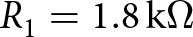 $R_1 = 1.8 \, \textrm{k}\Omega$,
 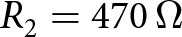 $R_2 = 470 \, \Omega$,
 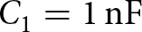 $C_{1} = 1 \, \textrm{n}\textrm{F}$, and
 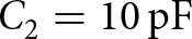 $C_{2} = 10 \, \textrm{p}\textrm{F}$. This network is also needed to stabilize the biasing source output impedance in the wide measurement bandwidth. In the “Circuit A” prototype, the RF transmission line carrying output noise power, and the supply line for filtered DC biasing current, are connected to the opposite emitter terminal pads of the discrete HBT package, which consists of a four-lead SMD TSFP-4-1. This design detail was exploited in the main radiometer board to improve physical and electrical separation of RF and DC signals within the PCB; this is however, non-optimal for the characterization because of the bias filtering network, which cannot be de-embedded from measurement results [Reference Badii, Collodi, Righini and Cidronali15].
The filtering and bypassing component values in “Circuit A” prototype proved to be non-optimal for mm-Wave band operation; the high-value resistors also limit the maximum biasing current to under  $7 \, \textrm{m}\textrm{A}$ because of the
  $15 \, \textrm{V}$ supply voltage limit for the level translator. The component values have been chosen as a starting point from another work [Reference Simoncini and Alimenti16], which analyzes a similar noise source prototype also built on a discrete HBT; the experimental characterization is however, limited to the lower C band.
From a characterization of the DUT output impedance, carried out by VNA measurements and a subsequent de-embedding procedure, the optimal value of the matching and filtering components that maximize output noise power or Excess Noise Ratio (ENR) in a given bandwidth can be estimated [Reference Duan and Wang8, Reference Collantes, Pollard and Sayed13, Reference Wong, Wong, Gorin and Lu14]. This is, however, unnecessary in this work, which analyzes temperature drift and mismatch error correction techniques in a general and wideband use case.
It is possible to recall the standard definition for the ENR, which will be employed in the following description,
 \begin{equation}
ENR \triangleq \frac{T_G^H - T_G^C}{290 \, \textrm{K}} \, ,
\end{equation}
\begin{equation}
ENR \triangleq \frac{T_G^H - T_G^C}{290 \, \textrm{K}} \, ,
\end{equation} where  $T_G^H$ and
  $T_G^C$ are respectively the Hot and Cold equivalent noise temperatures from the source. This simple relation is valid by supposing a perfectly impedance-matched setup, with no interconnection losses affecting the DUTs, at the standard
  $290 \, \textrm{K}$ IEEE reference temperature. The mentioned non-idealities will be corrected by a de-embedding procedure.
The “Circuit B,” employed for C and X band measurements, includes no biasing or decoupling network. The PCB is employed solely to physically support the active device and the RF connector, so an external bias-tee has been used during performance evaluation of this prototype. This setup allows a higher value of the maximum biasing current that can be injected in the BE junction during the test procedure, since no external resistive elements are present in the circuit. The configuration also allows the complete de-embedding of the active device up to the emitter terminal pad. In both noise source prototypes, the generated noise power is collected through a  $3.5\, \textrm{m}\textrm{m}$ coaxial connector, specified for a cut-off frequency of
  $40\, \textrm{G}\textrm{Hz}$ and an associated insertion loss of under
  $0.4\,\mathrm{dB}$. The employed PCB substrate is Rogers RO-4350B, the board is
  $254\, \unicode{x03BC}\textrm{m}$ thick [Reference Badii, Collodi, Righini and Cidronali15].
The “Circuit A” prototype was also employed for the temperature drift characterization, the latter carried out in the K band only [Reference Badii, Collodi, Righini and Cidronali15]. Because of that, a Texas Instruments TMP236 temperature sensor IC is located in this circuit, which is visible in Figure 2(a). This sensor monitors the PCB temperature, which is necessary for the subsequent thermal drift compensation of the noise power and, to maximize thermal coupling between the sensor package and the noise-generating HBT, the first one was physically placed as near as possible to the second one. The sensor is connected to the low thermal resistance ground plane by many via holes, also needed for output CPW line grounding; these also limit EM coupling between the two mentioned devices.
Description of the experimental setup
In the proposed work, the performances of the noise source prototypes were evaluated by two measurement stages. In one of them, spectral noise power distribution is considered and, after a de-embedding procedure, the maximum available ENR value, which is obtainable under ideal lossless and impedance-matched conditions, is provided.
During this procedure, which was repeated in “Circuit A” for the K band and in “Circuit B” for the C and X bands, an HP8564A spectrum analyzer was employed for data acquisition.
The aim of the second measurement stage, which was carried out only for the K band on “Circuit A,” is the characterization of generated noise thermal stability and its linearity over avalanche bias current, which is named I 0 in the following description [Reference Badii, Collodi, Righini and Cidronali15]. For this measurement step, a Keysight U2002A power meter was employed.
In both measurement stages, the output noise power from the DUT is expressed in terms of ENR, which was obtained by employing the Y-Factor procedure, which is widely adopted in literature for experimental noise performance estimation in single- and multi-port networks [Reference Wong, Wong, Gorin and Lu14, Reference Kang, Kim, Lee, Park and Kim17, Reference YiBin, Yulong and Yuhui18]. It ideally compensates for noise figure and insertion losses introduced by the measurement setup, if these effects remain unchanged between different measurements. Because of that, an extended form of the Y-factor method was employed to account for impedance mismatches and physical temperature differences between the DUT and the measurement setup blocks.
By considering two generic noise sources, namely  $S1$ and
  $S2$, which are inserted into a generic measurement setup as in Figure 3, it is possible to relate the ENR of both sources as
 \begin{equation}
\begin{aligned}
& ENR^{(S1)} + 10\log_{10}\left(\frac{Y_{OUT}^{(S2)}-1}{Y_{OUT}^{(S1)}-1}\right) \\
& \quad = ENR^{(S2)} + 10\log_{10}\left(\frac{T_{{IN}_{C}}^{(S1)}+ T_{EQ}}{T_{{IN}_{C}}^{(S2)}+ T_{EQ}}\right) \, ,
\end{aligned}
\end{equation}
\begin{equation}
\begin{aligned}
& ENR^{(S1)} + 10\log_{10}\left(\frac{Y_{OUT}^{(S2)}-1}{Y_{OUT}^{(S1)}-1}\right) \\
& \quad = ENR^{(S2)} + 10\log_{10}\left(\frac{T_{{IN}_{C}}^{(S1)}+ T_{EQ}}{T_{{IN}_{C}}^{(S2)}+ T_{EQ}}\right) \, ,
\end{aligned}
\end{equation}Block diagram of the measurement setup, for spectral, integrated-power, and thermal drift evaluation. The main variables include physical temperatures (blue), noise ones (red), and reflection coefficients (black).

where TEQ is the equivalent noise temperature at the measurement setup input,  $T_{{IN}_{C}}$ is the cold-state noise temperature delivered to the measurement setup input, as in Figure 3, which can be different between
  $S1$ and
  $S2$ because of DUT impedance mismatches (
 $\Gamma_S$) or non-equal physical temperatures (
 $T_0^D$); while
 \begin{equation}
Y_{OUT} \triangleq \frac{T_{OUT}^H}{T_{OUT}^C} \equiv \frac{T_{{IN}_{H}} + T_{EQ}}{T_{{IN}_{C}} + T_{EQ}} \, ,
\end{equation}
\begin{equation}
Y_{OUT} \triangleq \frac{T_{OUT}^H}{T_{OUT}^C} \equiv \frac{T_{{IN}_{H}} + T_{EQ}}{T_{{IN}_{C}} + T_{EQ}} \, ,
\end{equation} is defined as the Y-factor of the measured, output noise temperature from the setup chain. One of the two noise sources is defined as the reference for the Y-factor method, named REF; in the present work, this is a Keysight 346C standard noise source whose ENR, defined at the standard IEEE reference temperature of  $290 \, \textrm{K}$, is here named
  $\mathrm{ENR}^{R}$, and it is equal to
  $15.7\,\mathrm{dB}$ averaged in the
  $24-32 \, \textrm{G}\textrm{Hz}$ frequency range (K band), while for the C and X bands, the
  $\mathrm{ENR}^{R}$ is, respectively, equal to
  $18.0\,\mathrm{dB}$ averaged in the
  $4-6 \, \textrm{G}\textrm{Hz}$ frequency range and to
  $17.1\,\mathrm{dB}$ averaged in the
  $10-12 \, \textrm{G}\textrm{Hz}$ frequency range.
In the present analysis, because of differences between the DUT physical temperature,  $T_{0}^{D}$, and the REF one,
  $T_{0}^{R}$, the estimated ENR values from (2) should be compensated for that. Finally, due to DUT output and measurement setup input impedance mismatches, not only will the ENR be degraded because of return loss, but unwanted contributions arising from measurement setup physical temperatures will also be introduced, for example, that of the input attenuator, TA, visible in Figure 4, which is employed in the measurement setup of “Circuit A.” The measurement setup ambient temperature, T 0, will also affect the ENR results because of impedance mismatches. This is an effect which is not modeled in the simplified Y-factor method, which assumes instead perfectly matched blocks [Reference Vidyalakshmi and Arunachalam7, Reference Otoshi12, Reference Wong, Wong, Gorin and Lu14], and because of that, some considerations regarding these uncertainty sources have been provided in Section 3.1.
Experimental setup for spectral and integrated-power measurements in the K band, for the “Circuit A.” Preamplifier chain block diagram in (a). The output power meter (Keysight U2002A) is visible in (b).

In this measurement setup, the ENR stability over time is mostly dominated by the DUT self-heating errors, because of the avalanche current which alters the  $T_{0}^{D}$ locally at the EB junction. In order to reduce these effects, an automatic measurement procedure which applies narrow I 0 bursts was adopted, by switching the on-board high voltage level translator with an external control signal, for “Circuit A”; and by directly switching the VNS, for “Circuit B.”
Noise temperature transfer function, from DUT source to measurement setup
By considering the high-level block diagram of the measurement setup, in Figure 3, it is possible to see the main variables affecting measurement results, which are not considered in the conventional Y-Factor method of (2).
The black symbols represent impedance mismatch coefficients, the red ones represent equivalent noise temperatures, while the blue ones represent physical temperatures. Some variables are separately defined for DUT – (D) and REF – (R) sources, as indicated by the  $D/R$ superscript, but also for Hot – (H) and Cold – (C) noise-generating states, as indicated by the
  $H/C$ subscript. The same definition applies to the intrinsic noise generator temperature, TG, and its reflection coefficient
  $\Gamma_{G}$, while
  $\Gamma_{S}$ is the source one at the measurement setup input plane.
First, the noise source can be separated into an intrinsic noise generator and a linear loss network, located before the output measurement plane of the source. The loss network ( $\mathbf{S_L}$) S-parameters are defined for the DUT source only, the REF one is already de-embedded at the output connector by factory calibration so it was considered ideal.
The noise temperature delivered to the measurement setup input can be expressed as a combination of the generator temperature (TG), the device physical one (T 0) and also a reverse-flowing noise temperature (TR) which exists the measurement setup input towards the source,
 \begin{equation}
\begin{aligned}
T_{IN} &= \left[\frac{P_L}{P_{AVS}}\right] \cdot T_{G} + \left[\frac{P_{L}}{P_{AVN}}\right] \left[\frac{P_{AVS}-P_{AVN}}{P_{AVS}}\right] \cdot T_{0} \\
& \quad + \left[\frac{P_{AVN}-P_{L}}{P_{AVN}}\right] \cdot T_{R} \, ,
\end{aligned}
\end{equation}
\begin{equation}
\begin{aligned}
T_{IN} &= \left[\frac{P_L}{P_{AVS}}\right] \cdot T_{G} + \left[\frac{P_{L}}{P_{AVN}}\right] \left[\frac{P_{AVS}-P_{AVN}}{P_{AVS}}\right] \cdot T_{0} \\
& \quad + \left[\frac{P_{AVN}-P_{L}}{P_{AVN}}\right] \cdot T_{R} \, ,
\end{aligned}
\end{equation}which can be rewritten in the form [Reference Otoshi12],
 \begin{align}
T_{IN} = \alpha_{m} \Upsilon T_{G} + \alpha_{m} (1-\Upsilon) T_{0} + (1-\alpha_{m}) T_{R} \, ,
\end{align}
\begin{align}
T_{IN} = \alpha_{m} \Upsilon T_{G} + \alpha_{m} (1-\Upsilon) T_{0} + (1-\alpha_{m}) T_{R} \, ,
\end{align}by defining the αm and ϒ symbols as
 \begin{equation}
\begin{aligned}
&\Upsilon \triangleq \left[\frac{P_{AVN}}{P_{AVS}}\right] \leq 1 \quad , \quad \alpha_{m} \triangleq \left[\frac{P_{L}} {P_{AVN}}\right] \leq 1 \, , \\
&\Upsilon \cdot \alpha_{m} \triangleq \left[\frac{P_L}{P_{AVS}}\right] \leq 1 \, ,
\end{aligned}
\end{equation}
\begin{equation}
\begin{aligned}
&\Upsilon \triangleq \left[\frac{P_{AVN}}{P_{AVS}}\right] \leq 1 \quad , \quad \alpha_{m} \triangleq \left[\frac{P_{L}} {P_{AVN}}\right] \leq 1 \, , \\
&\Upsilon \cdot \alpha_{m} \triangleq \left[\frac{P_L}{P_{AVS}}\right] \leq 1 \, ,
\end{aligned}
\end{equation} where ϒ can be considered equivalent to the Available Gain (GA) from the Network, αm is a power mismatch factor between the noise source output and the measurement setup input,  $\Upsilon \cdot \alpha_{m} $ is equivalent to the Transducer Gain (GT),
 \begin{equation}
\Upsilon \equiv G_A = \frac{\bigr(1- \lvert{\Gamma_{G}}\rvert^2 \bigl) \cdot \lvert S_{21} \rvert^2}{\bigr(1- \lvert{\Gamma_{S}}\rvert^2 \bigl) \cdot \lvert 1-S_{11} \, {\Gamma_{G}} \rvert^2} \, ,
\end{equation}
\begin{equation}
\Upsilon \equiv G_A = \frac{\bigr(1- \lvert{\Gamma_{G}}\rvert^2 \bigl) \cdot \lvert S_{21} \rvert^2}{\bigr(1- \lvert{\Gamma_{S}}\rvert^2 \bigl) \cdot \lvert 1-S_{11} \, {\Gamma_{G}} \rvert^2} \, ,
\end{equation} \begin{equation}
\alpha_{m} = \frac{\bigr(1- \lvert{\Gamma_{I}}\rvert^2 \bigl) \cdot \bigr(1- \lvert{\Gamma_{S}}\rvert^2 \bigl)}{\lvert 1-\Gamma_{I} \, {\Gamma_{S}} \rvert^2} \, ,
\end{equation}
\begin{equation}
\alpha_{m} = \frac{\bigr(1- \lvert{\Gamma_{I}}\rvert^2 \bigl) \cdot \bigr(1- \lvert{\Gamma_{S}}\rvert^2 \bigl)}{\lvert 1-\Gamma_{I} \, {\Gamma_{S}} \rvert^2} \, ,
\end{equation} \begin{equation}
\Upsilon \alpha_{m} \equiv G_T = \frac{\bigr(1- \lvert{\Gamma_{I}}\rvert^2 \bigl) \cdot \lvert S_{21} \rvert^2 \cdot \bigr(1- \lvert{\Gamma_{G}}\rvert^2 \bigl)}{\lvert 1-\Gamma_{I} \, {\Gamma_{S}} \rvert^2 \cdot \lvert 1-S_{11} \, {\Gamma_{G}} \rvert^2} .
\end{equation}
\begin{equation}
\Upsilon \alpha_{m} \equiv G_T = \frac{\bigr(1- \lvert{\Gamma_{I}}\rvert^2 \bigl) \cdot \lvert S_{21} \rvert^2 \cdot \bigr(1- \lvert{\Gamma_{G}}\rvert^2 \bigl)}{\lvert 1-\Gamma_{I} \, {\Gamma_{S}} \rvert^2 \cdot \lvert 1-S_{11} \, {\Gamma_{G}} \rvert^2} .
\end{equation} The three quantities are less or equal to unity since the  $\mathbf{S_L}$ network in Figure 3 is passive. As it will be shown in the following description, the only relevant term in this analysis is αm, (7b), with particular concern at its denominator since the
  $|1- \Gamma_I \, \Gamma_S|$ term gives rise to frequency ripple in the ENR spectral distribution, which should be compensated because it is due to the measurement setup only [Reference Collantes, Pollard and Sayed13].
Description of measurement procedures
The different measurement procedures employed, which include total-power (frequency integrated) and spectral power distribution of the noise generated signal, were chosen because of different requirements of accuracy, resolution, and measurement speed needed for the maximum available ENR estimation and thermal drift analysis measurement stages, respectively. By recalling Figure 3, the output plane of the preamplifier and biasing network was connected alternatively to the SA or to the power meter. The possible differences in impedance mismatch observed at the setup output plane do not affect the measurements, since this issue is totally compensated after system normalization, by the Y-factor method [Reference Alimenti, Simoncini, Brozzetti, Maistro and Tiebout4, Reference Alimenti, Tasselli, Botteron, Farine and Enz6]. Since the U2002A power meter is characterized for a  $10 \, \textrm{MHz}-26.5 \, \textrm{GHz}$ measurement bandwidth, in the K band setup, the instrument was normalized by comparison with the HP8564 SA response, by considering the whole cascade, including the input bandpass-filter, as shown in Figures 3 and 4(b). This procedure is unnecessary for the C and X band setup, shown in Figure 5. In Figure 6, the frequency response of such cascade is illustrated, where the pass-band insertion loss was normalized at
  $0\,\mathrm{dB}$ by comparison with the SA response, which was considered flat as the instrument covers a
  $40 \, \textrm{GHz}$ bandwidth. The zero value is not critical since the Y-factor compensates for gain errors in TOUT estimation. From Figure 6, the pass-band of the filter and power-meter cascade is sufficient to evaluate measurements inside the
  $24-32 \, \textrm{GHz}$ frequency range, since the equivalent noise bandwidth characterizes this measurement, and it covers the aforementioned frequency range.
Experimental setup for spectral noise power measurements in the C and X bands, for the “Circuit B.” The amplifying and DC biasing chain includes an input circulator (*), which can be employed for the C band measurements only to better evaluate mismatch-introduced errors.

Frequency response of the bandpass filter and cascaded U2002A power meter ( $A_{PD}(f)$), normalized by comparison with the HP8564A SA frequency response (
 $A_{SA}(f)$), as in Figure 3.

Introduction of K band measurements for the “Circuit A”
In the K band measurement setup, visible in Figure 4, some simplifying assumptions have been made. First, a  $6\,\mathrm{dB}$ attenuator has been placed at the measurement setup input plane. This component reduces the risk of possible LNA instabilities due to the mismatched DUT noise source; it also lowers the
  $\Gamma_{I}$ setup reflection coefficient at the same plane [Reference Otoshi12, Reference Kang, Kim, Lee, Park and Kim17]. Thanks to this attenuator, the magnitude of the undefined reverse noise temperature TR is reduced by the A attenuation factor; a fraction of its physical temperature TA is also added to the equivalent input one (TEQ),
 \begin{equation}
T_R = \frac{T'_R}{A} + T_A \cdot \left(1-\frac{1}{A}\right) \sim T_A \, ,
\end{equation}
\begin{equation}
T_R = \frac{T'_R}{A} + T_A \cdot \left(1-\frac{1}{A}\right) \sim T_A \, ,
\end{equation} where  $T'_R$ is the reverse noise temperature entering the attenuator, from the first LNA input. Thanks to a sensor physically located on the attenuator body, as visible in Figure 4, the TA can be accurately monitored also during the DUT board heating in the temperature drift analysis measurements [Reference Kang, Kim, Lee, Park and Kim17, Reference YiBin, Yulong and Yuhui18]. In the following description, the attenuator temperature difference over the ambient one proved to be negligible, so the
  $T_{A}=T_{0}$ simplifying assumption was accepted.
By recalling the (5), after supposing  $T_{R} \approx T_{A} = T_{0}$, it is possible to employ the grouped mismatch and loss coefficients only, defined in (7c), which are named as
  $(\alpha_{m} \Upsilon) \triangleq M_{j}^{i}$ for convenience,
 \begin{equation}
M_{H/C}^{D/R} \overset{\Delta}{=} \frac{\bigr(1- \lvert{\Gamma_{G}}_{H/C}^{D/R}\rvert^2 \bigl) \cdot \bigr(1-\lvert \Gamma_{I} \rvert^2 \bigl) \cdot \lvert S_{21} \rvert^2}{\lvert 1-{\Gamma_{S}}_{H/C}^{D/R} \, \Gamma_{I} \rvert^2 \cdot \lvert 1-S_{11} \, {\Gamma_{G}}_{H/C}^{D/R} \rvert^2} ,
\end{equation}
\begin{equation}
M_{H/C}^{D/R} \overset{\Delta}{=} \frac{\bigr(1- \lvert{\Gamma_{G}}_{H/C}^{D/R}\rvert^2 \bigl) \cdot \bigr(1-\lvert \Gamma_{I} \rvert^2 \bigl) \cdot \lvert S_{21} \rvert^2}{\lvert 1-{\Gamma_{S}}_{H/C}^{D/R} \, \Gamma_{I} \rvert^2 \cdot \lvert 1-S_{11} \, {\Gamma_{G}}_{H/C}^{D/R} \rvert^2} ,
\end{equation}The TIN in (5) can also be redefined as
 \begin{equation}
{T_{IN}}_{H/C}^{D/R} \overset{\Delta}{=} M_{H/C}^{D/R} \cdot {T_{G}}_{H/C}^{D/R} + \bigl(1-M_{H/C}^{D/R} \bigr) \cdot T_{0} \, ,
\end{equation}
\begin{equation}
{T_{IN}}_{H/C}^{D/R} \overset{\Delta}{=} M_{H/C}^{D/R} \cdot {T_{G}}_{H/C}^{D/R} + \bigl(1-M_{H/C}^{D/R} \bigr) \cdot T_{0} \, ,
\end{equation}which is the noise power transfer function, employed for the characterization of “Circuit A” prototype.
Introduction of C and X band measurements for the “Circuit B”
In order to validate the feasibility of the Noise Source in a wideband environment, a characterization of the generated noise power performance has also been evaluated in the C and X bands, by employing “Circuit B” prototype. This measurement stage does not consider thermal drift analysis, as already done in the “Circuit A” prototype, so a power-integrated measurement procedure was not made.
In the C and X band measurement setup, which is visible in Figure 5, a connectorized bias-tee (Mini Circuits ZFBT-6G-FT+) was employed for the external HBT biasing, since the prototype does not include any DC bias filter or bypass network. For the C band measurements only, a circulator connected as an isolator with the third port terminated into a matched load was also used. This device is a Raditek RADC-5.75-5.85 and was placed between the bias-tee and the first LNA input; it was used to lower the  $\Gamma_I$, since the employed LNAs (HMC441) are characterized for a working frequency bandwidth of
  $6-18 \, \textrm{GHz}$ and therefore are substantially mismatched in the lowest part of the tested bandwidth, starting at
  $4 \, \textrm{GHz}$, as it can be seen in Figure 7(a). This also allows the validation of mismatch error compensation, described in the following subsection [Reference Duan and Wang8, Reference Otoshi12, Reference Collantes, Pollard and Sayed13].
Input reflection coefficient (a) for the C and X band setup of Figure 5; the circulator was employed for C band only. PCB and connection losses between the HBT and measurement setup input planes (b), for “Circuit B.”

The TIN and the loss coefficient  $M_{H/C}^D$ definitions are exactly the same ones as those employed for the K band characterization, in (10) and (9), respectively. In Figure 8 it is possible to see the I 0-to-VEB response of the avalanche-driven HBT junction, as well as the associated DC biasing power PDC and the differential resistance RDC.
DC characteristics of the avalanche-driven EB junction, for the “Circuit B.” The I 0-to-VEB relation is shown in (a), while biasing power and DC differential resistance are shown in (b) as function of VEB.

Spectral distribution measurements and de-embedding
By considering “Circuit A” and “Circuit B” prototypes, the one-port de-embedding procedure was carried out in the DUT source PCB by connecting reference open, short and matched loads at the emitter pad of the unmounted HBT, at one end of the output transmission line. The procedure is useful in removing losses associated with DC bypass components, RF connector and PCB substrate material but, with regard to “Circuit A” only, it does not extract loss contributions arising from the RC filtering network, physically located at the other HBT emitter pad as well as the whole HBT package parasitics, which are here considered as an intrinsic part of the source. In Figure 9, it is possible to see two DUT source reflection coefficients before and after the de-embedding procedure, recorded at two extreme I 0 points of  $240\, \unicode{x03BC}\textrm{A}$ and
  $6.71\, \textrm{m}\textrm{A}$ respectively, which are named
  ${\Gamma_{S}}_{H}^{D}$ and
  ${\Gamma_{G}}_{H}^{D}$ by looking at Figure 3. The first one is directly measured by the VNA, while the second one is extracted by employing the calculated loss network matrix, which includes the whole mentioned losses and mismatch contributions between the HBT emitter pad and the prototype output reference plane, which is also equal to the VNA input one. Due to the limited bandwidth of the instrument, this de-embedding procedure was provided in a
  $24.5-26.5\, \textrm{G}\textrm{Hz}$ frequency range.
“Circuit A” output reflection coefficients at I 0 measurement extremes, for the K-band in a  $24.5-26.5 \, \textrm{G}\textrm{Hz}$ bandwidth [Reference Badii, Collodi, Righini and Cidronali15]. Measured (a) and de-embedded (b).

In Figure 10, the  ${\Gamma_{G}}_{H}^{D}$ is shown for “Circuit B”; the results are de-embedded from PCB and interconnection losses (Figure 7(b)) in the
  $3.5-12\, \textrm{G}\textrm{Hz}$ frequency range for a
  $V_{EB} = V_{NS}$ spanning in the
  $4.00-5.50 \, \textrm{V}$ range.
“Circuit B” measured output reflection coefficients in the  $4.00-5.50 \, \textrm{V}$ bias voltage, for the
  $3.5-12 \, \textrm{GHz}$ bandwidth. Magnitudes (b) include a dashed curve of the resistive-only mismatch calculated with RDC (Figure 8(b)).

In Figure 10(b), the  ${\Gamma_{G}}_{H}^{D}$ magnitudes are reported; the dashed curve includes calculated values by employing the DC junction differential resistance (RDC) in Figure 8(b). Considering an unmatched source operation, it is possible to identify an optimal value of bias voltage (
 $V_{EB, \, opt}$) of
  $4.8-5.0 \, \textrm{V}$, at an avalanche current of
  $5-7 \, \textrm{mA}$, which minimizes the noise source return loss; this can be useful for the unmatched operation of the DUT, up to the X band.
For “Circuit B,” it is not generally possible to say that  $T_{R} \approx T_{0}$ when the circulator is not employed, because of the lack of a wideband resistive attenuator before the preamplifier network, which is instead used during “Circuit A” testing [Reference Vidyalakshmi and Arunachalam7, Reference Duan and Wang8, Reference Kang, Kim, Lee, Park and Kim17]. In this case, by recalling the (5), the difference between hot and cold state noise temperatures, from the DUT source to the measurement setup input, can be expressed as
 \begin{equation}
\begin{aligned}
\Delta {T}_{IN}^{D} &= \alpha_{{m}_{H}} \Upsilon_H \cdot \Delta T_{G}^{D} \\
&+ (\alpha_{{m}_{H}} - \alpha_{{m}_{C}}) \cdot (T_{0}^{D}-T_{R}) \, ,
\end{aligned}
\end{equation}
\begin{equation}
\begin{aligned}
\Delta {T}_{IN}^{D} &= \alpha_{{m}_{H}} \Upsilon_H \cdot \Delta T_{G}^{D} \\
&+ (\alpha_{{m}_{H}} - \alpha_{{m}_{C}}) \cdot (T_{0}^{D}-T_{R}) \, ,
\end{aligned}
\end{equation} where it is possible to see the unknown  $(T_{0}^{D}-T_{R})$ contribution affecting the measurement results, especially for low values of
  $T_G^D$. This effect is not compensated by the conventional Y-Factor method; so it affects the measurement results if not accounted for. In reality, it is possible to estimate this quantity by measuring output noise power from the measurement setup, by replacing the DUT source alternatively with matched and short loads, since in these cases we have αm = 1 and αm = 0, respectively [Reference Otoshi12]. The matched/short characterization was made in both X and C band, the latter by using “Circuit B” with and without input circulator. The resulting shift in output noise power was recorded to be under
  $0.5\,\mathrm{dB}$, which is a value comparable to the SA accuracy, so the assumption that
  $T_{R} \approx T_{0}$ was employed even in this analysis. Another reason for the approximation is that the quantity
  $ \left(\alpha_{{m}_{H}} - \alpha_{{m}_{C}} \right)$ in (11) is maximum near
  $V_{EB, \, opt}$, when the difference between
  $\lvert \Gamma_{G_{H}}^D \rvert$ and
  $\lvert \Gamma_{G_{H}}^D \rvert \sim 1$ is also maximum, by recalling Figure 10(b). This is also the point near the peak of
  $T_G^D$, as it can be seen from Figures 11 and 12, so the
  $(T_{0}^{D}-T_{R})$ influence on ENR estimation is negligible.
C band ENR spectral distribution, for “Circuit B” in a  $4-6 \, \textrm{G}\textrm{Hz}$ bandwidth, at
  $T_{0}^{D} = 21 \, ^\circ\textrm{C}$. The averaged result is shown considering the same bandwidth. Results in (a) include mismatch and loss compensation of the source, in (b) no compensation was done.

X band ENR spectral distribution, for “Circuit B” in a  $10-12 \, \textrm{G}\textrm{Hz}$ bandwidth, at
  $T_{0}^{D} = 21 \, ^\circ\textrm{C}$. The averaged result is shown considering the same bandwidth. Results in (a) include mismatch and loss compensation of the source, in (b) no compensation was done.

In order to estimate the maximum available DUT output temperature ( $T_{G}^{D}$), defined at the Emitter pad of the HBT, an indirect procedure was employed, for both prototypes, as follows. By using the
  $\lvert S_{21} \rvert^2$ from the calculated loss network matrix of Figure 3 and the experimentally derived
  $\Gamma_{G}^{D}$ and
  $\Gamma_{S}^{D}$ in Figures 9 and 10, the
  $M^{D}_{H/C}$ loss coefficients in (9) can be completely defined for the DUT source,
 \begin{equation}
M_{H/C}^{D/R} \approx \bigr(1- \lvert{\Gamma_{G}}_{H/C}^{D/R}\rvert^2 \bigl) \cdot \lvert S_{21} \rvert^2 \, ,
\end{equation}
\begin{equation}
M_{H/C}^{D/R} \approx \bigr(1- \lvert{\Gamma_{G}}_{H/C}^{D/R}\rvert^2 \bigl) \cdot \lvert S_{21} \rvert^2 \, ,
\end{equation} where, as a simplifying assumption, a negligible reflection coefficient  $\Gamma_{I}$ is supposed at the attenuator input of the K band setup (Figure 4), since the
  $-10\,\mathrm{dB}$ worst-case input return loss of the HMC1040 LNA and the added
  $6\,\mathrm{dB}$ attenuation. For the C and X band setup of Figure 4, the
  $\Gamma_{I}$ were accurately measured to evaluate a possible impedance mismatch correction [Reference Duan and Wang8, Reference Meys and Boukerroum10, Reference Diebold, Weissbrodt, Massler, Leuther, Tessmann and Kallfass19]. The results are illustrated in Figure 7(a).
It was also supposed that all physical temperatures in the whole measurement setup were equal to the ambient one, which was recorded at  $T_{0} = 21 \, ^\circ\textrm{C}$, thanks to the switching operation of the biasing source (VNS), which helps in reducing the DUT junction self-heating errors, as described in Section 3.
The fitting procedure is iterative; a hot-state (DUT switched on)  ${T_{G}}_{H}^{D}$ can be estimated and this value, applied to (10) with the known loss contribution, for example Figure 7(b) for “Circuit B,” should ensure that the resulting
  $T_{IN}^{D}$ (loss-affected) fits with the experimental data obtained by spectral power measurements.
For K band, in “Circuit A,” this is shown in Figure 13, where the resulting data is presented in terms of  $\mathrm{ENR}^{D}_{(f)}$ along with the best fittings. The results are frequency-limited in the mentioned instrument bandwidth; after the procedure a frequency-averaged fitting error of under
  $0.3\,\mathrm{dB}$ has been observed. For C and X band measurements in “Circuit B,” an additional procedure is needed to complete the de-embedding in this prototype because of the significant
  $\Gamma_I$. By recalling the loss coefficients (9), after applying the Y-Factor method, a multiplying factor remains to be compensated
 \begin{equation}
\frac{M_{H/C}^{D}}{M_{H/C}^{R}} \approx \frac{\bigr(1- \lvert{\Gamma_{G}}_{H/C}^{D}\rvert^2 \bigl) \cdot \lvert S_{21} \rvert^2}{\lvert 1-{\Gamma_{S}}_{H/C}^{D} \, \Gamma_{I} \, e^{\, j 2 \beta l} \rvert^2 } \, ,
\end{equation}
\begin{equation}
\frac{M_{H/C}^{D}}{M_{H/C}^{R}} \approx \frac{\bigr(1- \lvert{\Gamma_{G}}_{H/C}^{D}\rvert^2 \bigl) \cdot \lvert S_{21} \rvert^2}{\lvert 1-{\Gamma_{S}}_{H/C}^{D} \, \Gamma_{I} \, e^{\, j 2 \beta l} \rvert^2 } \, ,
\end{equation}ENR spectral power distribution, from “Circuit A” measurements in K-Band [Reference Badii, Collodi, Righini and Cidronali15]. The source was biased at two I 0 in the  $24.5-26.5 \, \textrm{G}\textrm{Hz}$ bandwidth. Maximum available ENR was obtained by estimating a
  $T_{G}^{D}$ in (10) for which the best fitting is achieved between the calculated (loss-affected)
  $T_{IN}^{D}$ and the measured one.

where  $\lvert S_{21} \rvert^2$ is corrected with the loss matrix (Figure 7(b)) as in the previous K band procedure, while
  $e^{\, j 2 \beta l}$ represents a possible measurement error in reflection coefficient phases, modeled by a length (l) of transmission line between DUT output and measurement setup input planes. The
  $\lvert 1-{\Gamma_{S}}_{H/C}^{D} \, \Gamma_{I} \, e^{\, j 2 \beta l}\rvert$ term is critical, since phase errors give rise to an erroneous ripple in the
  $ENR_{(f)}^D$ estimation. In this case, a fitting procedure was employed, by estimating a
  $(2 \beta l)$ phase term for which the
  $ENR_{(f)}^D$ peak-to-average ratio is reduced in a given bandwidth. Such results are visible in Figure 14(a) and (b), where a ripple under
  $\pm \, 1 \, \textrm{dB}$ still remains at the extreme VBE where the mismatch is higher.
C band (a) and X band (b) ENR spectral distribution, for “Circuit B,” in the  $4 - 6 \, \textrm{G}\textrm{Hz}$ and
  $10 - 12 \, \textrm{G}\textrm{Hz}$ frequency ranges, respectively. The device temperature is constant at
  $T_{0}^{D} = 21 \, ^\circ\textrm{C}$. All values are corrected by considering source and measurement setup mismatches.

The  ${T_{G}}_{H}^{D}$ noise temperatures calculated after these procedures are considered the maximum available from the HBT device, in a lossless and perfectly matched environment [Reference Otoshi12, Reference Collantes, Pollard and Sayed13]. When estimating the maximum
  $\mathrm{ENR}^{D}_{(f)}$, a magnitude decay of ω −2 was also included, this is necessary due to the physical model of avalanche noise current spectral density in semiconductors, which presents a similar decay [Reference Gupta5, Reference Hines20],
 \begin{equation}
\langle \, \overline{i_{na}} \, \rangle^{2}=\frac{2q\, I_{0}}{\omega^{2} \; \tau_{x}^{2}},
\end{equation}
\begin{equation}
\langle \, \overline{i_{na}} \, \rangle^{2}=\frac{2q\, I_{0}}{\omega^{2} \; \tau_{x}^{2}},
\end{equation}where I 0 is the breakdown current and τx is the average time between two ionizations. However, no further assumptions can be made with (14) model; it cannot be used to obtain the theoretical noise power here, because the equivalent admittance appearing in parallel to the ina noise current generator cannot be extracted in this work due to the need of a very accurate model concerning HBT package parasitics, which was not available at the time; this can be efficiently done in integrated processes instead [Reference Alimenti, Simoncini, Brozzetti, Maistro and Tiebout4, Reference Alimenti, Tasselli, Botteron, Farine and Enz6].
After considering the maximum  $I_{0} = 6.71\, \textrm{m}\textrm{A}$ for “Circuit A” prototype, a maximum available
  $\mathrm{ENR}^{D}_{(f)}$ between 16.2 and
  $15.5\,\mathrm{dB}$ was estimated for the
  $24.5-26.5\, \textrm{G}\textrm{Hz}$ frequency range, as reported in Figure 13.
For the “Circuit B” prototype, by considering a bias  $V_{EB} = 5.1 \, \textrm{V}$ and a
  $I_{0} = 6.9 \, \textrm{mA}$, a maximum available
  $\mathrm{ENR}^{D}_{(f)}$ between 25.6 and
  $24.8\,\mathrm{dB}$ was estimated for the
  $4-6\, \textrm{G}\textrm{Hz}$ frequency range (C band); while for the X band the same quantity varies between 22.6 and
  $22.1\,\mathrm{dB}$ in the
  $10-12\, \textrm{G}\textrm{Hz}$ frequency range. The mentioned data is shown in Figures 11(a) and 12(a), respectively.
The  $I_{0} = 6.9 \, \textrm{mA}$ is also the optimum bias for which the not-mismatch-compensated
  $\mathrm{ENR}^{D}_{(f)}$ peaks, at
  $24.1-23.1$ and
  $20.8-19.7\,\mathrm{dB}$ for the C and X band, respectively, as in Figures 11(b) and 12(b). The noise source matching is good at this bias point, because of the optimum RDC, Figure 8(b), allowing a satisfactory wideband operation of the noise source in the tested bandwidth, even without additional impedance matching, Figure 10(b).
Integrated noise power measurements and thermal stability considerations
This measurement procedure was employed for the K band only, by using “Circuit A” prototype. The measurement setup is shown in Figures 3 and 4. The filter, power-meter cascade replace the SA at the preamplifier output plane. A total-power measurement allows a better resolution in estimating noise power drifts during the thermal stability evaluation. Since measurement bandwidth exceeds that of the N5242A VNA, no de-embedding was applied to these results; the loss network contribution is here considered as an intrinsic part of the DUT source; the generated output noise temperature and ENR are referenced at the RF-output plane in Figure 2(a). The noise is power-integrated in the  $24-32 \, \textrm{G}\textrm{Hz}$ bandwidth and no impedance mismatch compensation has been made, so these results, defined
  $\overline{\mathrm{ENR}}^{D}$ here, should not be related to
  $\mathrm{ENR}^{D}_{(f)}$, illustrated in Figure 13, which are instead frequency-punctual.
The measuring procedure started with a linearly-variable I 0 current, the DUT physical temperature ( $T_{0}^{D}$) is a parameter which was changed after every I 0 sweep, by physically heating the prototype PCB. To obtain the best measurement accuracy, the physical temperature of the DUT, REF sources and every device in the measuring chain should be the same, like in the previous section discussion, since the off-state noise temperature at the measuring chain input,
  ${T_{IN}}_{C}^{D}$, would be equal to
  $T_{0}^{D}=T_{0}=T_{A}$, independently of reflection coefficients, as shown considering the (10). However, this state is unfeasible in the measurement procedure, so the DUT only was heated at
  $T_{0}^{D} \geq T_{0}=T_{A}$ and some error arising from
  $T_{0}^{D}$ difference should be expected.
The differences in loss-affected output noise temperatures between hot and cold states, evaluated at the attenuator input plane, Figure 4(a), are obtained by rearranging (10) and are necessary for Y-factor calculation. These values are now defined as
 \begin{equation}
\Delta {T}_{IN}^{D} = M_{H}^{D} \cdot \Delta T_{G}^{D} + (M_{H}^{D} - M_{C}^{D}) (T_{0}^{D}-T_{0}) ,
\end{equation}
\begin{equation}
\Delta {T}_{IN}^{D} = M_{H}^{D} \cdot \Delta T_{G}^{D} + (M_{H}^{D} - M_{C}^{D}) (T_{0}^{D}-T_{0}) ,
\end{equation} where  $T_{0}^{R}=T_{0}$. Statistical independence among thermal noise power (
 $T_{0}^{D/R}$) and avalanche-generated one (
 $\Delta T_{G}^{D/R}$) was also supposed, so
  ${T_{G}}_{H}^{D/R}$ =
  $\bigl(T_{0}^{D/R}+\Delta T_{G}^{D/R}\bigr)$ [Reference Gupta5, Reference Hines20]. For the REF noise source
 \begin{equation}
\Delta {T}_{IN}^{R} = M_{H}^{R} \cdot \Delta T_{G}^{R} .
\end{equation}
\begin{equation}
\Delta {T}_{IN}^{R} = M_{H}^{R} \cdot \Delta T_{G}^{R} .
\end{equation} From (15) it is possible to see the DUT physical temperature ( $T_{0}^{D}$) affecting measurement results, an effect originating from impedance mismatch and especially its fluctuations between hot and cold states. At the REF source’s output (16), a good matching and a negligible
  $\Gamma_{S}^{R}$ fluctuation between hot and cold states are supposed, so
  $M_{H}^{R} \approx M_{C}^{R} \approx (1- |\Gamma_{I}|^2)$. This term is removed after applying the Y-factor method since it is common to
  $M_{H/C}^{D}$ and
  $M_{H/C}^{R}$.
It should be recalled that in this setup (Figure 2(a)), the LNA input return loss, which is not worse than  $-10\,\mathrm{dB}$ as specified by the HMC1040 datasheet, is further improved at the
  $\Gamma_{I}$ plane by
  $-12\,\mathrm{dB}$ because of the matching pad. The mismatch error is temperature-linear in the first approximation, so it can be compensated in real-time thanks to the TMP236 on-board temperature sensor.
The reduction in output noise performance ( $\Delta T_{IN}^{D}$) due to
  $M_{H}^{D}$ is undesired, but it is not an accuracy concern; since DUT mismatch is mainly bias-dependent, with values shown in Figure 9, it can be included inside the
  $\mathrm{ENR}-I_{0}$ dependency when defining the fitting model. In Figure 15, the
  $\overline{\mathrm{ENR}}^{D}$ values are shown, for two I 0 sweeps and after considering the
  $T_{0}^{D}$ extremes in the range
  $21-102 ^\circ\textrm{C}$. The non-calibrated
  $\overline{\mathrm{ENR}}^{D}$ magnitude stability over ambient temperature was poor, as the recorded maximum drift was approximately
  $0.8\,\mathrm{dB}$ at the
  $I_{0} = 6.71\, \textrm{m}\textrm{A}$ and
  $T_{0}^{D}$ extremes, where an associated ENR of 10.8 dB was reported. This quantity translates to an error of
  $\pm 293\, \textrm{K}$ at the highest
  ${T_{G}}_{H}^{D} = 3470\, \textrm{K}$, which could be unacceptable even for an industry-oriented use-case [Reference Thomsen3, Reference Duan and Wang8, Reference Thompson, Rogers and Davis11].
 $\overline{\mathrm{ENR}}^{D} \, (\textrm{dB})$ obtained after integrated-power measurement in a
  $24-32 \textrm{G}\textrm{Hz}$ bandwidth;
  $T_{0}^{D}$ at the extremes of
  $21 - 102 \, ^\circ\textrm{C}$ (a). Relative error, estimated for the proposed fitting model (b), in the same conditions [Reference Badii, Collodi, Righini and Cidronali15].

The fitting law was chosen after considering the hypotheses mentioned in (14), (15), and (16); the proposed model is composed of three parts. The main term  $f_{1}(I_{0})$ is dominated by the DC bias current as in (14) [Reference Gupta5, Reference Hines20],
 \begin{equation}
\begin{aligned}
&f_{1}(I_{0}) \propto \Delta {T}_{G}^{D} \propto \langle \, \overline{i_{na}} \, \rangle^{2} \propto I_0^\alpha \\
&ENR_{(dB)}^D \propto c \, \log(I_0) \, ,
\end{aligned}
\end{equation}
\begin{equation}
\begin{aligned}
&f_{1}(I_{0}) \propto \Delta {T}_{G}^{D} \propto \langle \, \overline{i_{na}} \, \rangle^{2} \propto I_0^\alpha \\
&ENR_{(dB)}^D \propto c \, \log(I_0) \, ,
\end{aligned}
\end{equation} where α and c are fitting constants. The remaining terms  $f_{2}(I_{0})$ and f 3 were employed to account for ambient temperature drift effects, where a first-order relation was supposed,
 \begin{equation}
f_{2}(I_{0}) \, , \, f_{3} \propto \Delta ENR_{(dB)}^D \propto (a \cdot I_0 + b) \cdot T_0^D \, ,
\end{equation}
\begin{equation}
f_{2}(I_{0}) \, , \, f_{3} \propto \Delta ENR_{(dB)}^D \propto (a \cdot I_0 + b) \cdot T_0^D \, ,
\end{equation} where a and b are also fitting constants. This term is necessary because of  $\Gamma_{S}^{D}$ and
  $\Gamma_{G}^{D}$ that are not only I 0-dependent, but also
  $T_{0}^{D}$-dependent, so the latter cannot be separated. It is also necessary to recall avalanche breakdown physics, where noise-generated spectral current density as seen in (14) slightly decreases with junction temperature because τx increases with it [Reference Alimenti, Simoncini, Brozzetti, Maistro and Tiebout4–Reference Alimenti, Tasselli, Botteron, Farine and Enz6].
Finally, in Figure 15 it is also possible to see the relative error in the  $\overline{\mathrm{ENR}}^{D}$ magnitude fitting estimation, where an average value of
  $0.6\, \%$ is reported, and that means an amplitude of the error interval of
  $0.05\,\mathrm{dB}$ when the same maximum
  $T_{0}^{D}$ and I 0 ranges are considered. The minimum error at
  $I_{0} = 5.8\, \textrm{m}\textrm{A}$ is
  $0.23\, \%$, or 0.022 dB. The relative error is also shown for the
  $T_{G}^{D}$ estimation, where an average value of
  $1.7\, \%$ was obtained in the considered setup. The minimum relative error of
  $0.92\, \%$, or
  ${T_{G}}_{H}^{D}$ =
  $(3031 \pm 14) \, \textrm{K}$, was obtained at
  $I_{0} = 5.8\, \textrm{m}\textrm{A}$.
At the end of this analysis, by employing Table 1 model, the evaluated relative drift error is comparable to instrumentation accuracy, so the proposed calibration law proves to be effective. In a real use-case, where the employed devices are generally located in a single-PCB system, the temperature-related errors could also be lower, because of the reduced physical temperature gradients between circuit components, in such environment.
 $\overline{\mathrm{ENR}}^{D}$ current and temperature fitting parameters, defined at
  $T_{0}=21\, ^\circ\textrm{C}$ for the “Circuit A” [Reference Badii, Collodi, Righini and Cidronali15]

The  $\overline{\mathrm{ENR}}^{D}$ magnitude degradation due to mounting board, interconnection and impedance mismatch losses are here significant, as observed by comparing the unmatched, power-integrated results in Figure 15 with the spectral, de-embedded
  $\mathrm{ENR}^{D}_{(f)}$ results in Figure 13, by looking at Section 4.3.
The resulting DUT noise source accuracy can be considered acceptable for practical industrial applications, for example in industrial radiometer systems such as the Dicke-based ones, which require noise temperature reference with noise temperature comparable to the target temperature range [Reference Thomsen3, Reference Hach9, Reference Thompson, Rogers and Davis11].
Repeatability considerations
In order to characterize the repeatability of a noise source built on the proposed technology, an additional measurement phase employing power-integrated noise estimation has been made. These results, here defined as  $\overline{\mathrm{ENR}}^{D}$, are obtained from “Circuit B” prototype in a
  $4-6 \, \textrm{G}\textrm{Hz}$ bandwidth, by employing the measurement procedures illustrated in Section 4.3. The environment temperature was also recorded during the whole measurement phase; it was constant at
  $T_{0}^{D} = 21 \, ^\circ\textrm{C}$.
The results are shown in Figure 16; the original source, here named “DUT 1,” which is also the one employed for “Circuit B” characterization in the previous sections, is reported by using dashed lines for compensated and non-compensated ENR results as well as for the junction DC characteristics. The other nine DUTs are obtained after having replaced the source HBT with an equivalent one (BFP620F by Infineon) taken randomly from a different production lot. The aforementioned data is also summarized in Table 2, by considering the average value and measurement uncertainty for each quantity.
Repeatability of  $\overline{\mathrm{ENR}}^{D}$ (integrated-power) performances, for “Circuit B” in the
  $4-6 \, \textrm{G}\textrm{Hz}$ bandwidth at
  $T_{0}^{D} = 21 \, ^\circ\textrm{C}$, considering a sample of 10 BFP620F HBTs. Mismatch and loss compensated results in (a), no compensated results in (b). Junction DC characteristics in (c).

A significant difference in the DC junction characteristics is observable from Figure 16(c), in both avalanche knee voltage and differential resistance quantities, especially by considering the “DUT 1” trace, which comes from an older production lot. This effect translates to a discrepancy in the  $\overline{\mathrm{ENR}}^{D}$-to-VEB relation, as visible in Figure 16(a) and 16(b). The optimum bias voltage (
 $V_{EB, \, opt}$) for the unmatched operation (cf. Figure 10(b)) is also shifted because of the knee voltage spread; the average value is
  $4.92 \, \textrm{V}$ with an associated avalanche current of
  $I_0 \approx 10 \, \textrm{mA}$, slightly higher than the estimated
  $5-7 \, \textrm{mA}$ for “DUT 1,” in Section 4.3.
By considering the  $\max (\overline{\mathrm{ENR}}^{D})$ performances, reported in Table 2, obtained after measuring random DUTs from two production lots, the resulting data is compatible with the previous estimations in Section 4.3, where only the single “DUT 1” was considered. However, the associated uncertainty could be excessive in a precision use-case, so an initial calibration of the generated noise power level may be generally required in such applications, when a random active device is chosen from a production lot.
Maximum  $\overline{\mathrm{ENR}}^{D}$ performance, from results in Figure 16. The I 0 and VEB are measured at the
  $\max (\overline{\mathrm{ENR}}^{D})$ point

Conclusions
This paper has dealt with the operation principle and the wideband characterization of a multi-purpose, low-cost, temperature calibrated noise source built with Commercial Off-The-Shelf (COTS) components [Reference Badii, Collodi, Righini and Cidronali15]. Two prototype boards were developed and discussed, both using the same BFP620F HBT. The complete analysis has covered the C, X, and K bands, in the frequency ranges of respectively  $4-6$,
  $10-12$, and
  $24-32 \, \textrm{G}\textrm{Hz}$. In Table 3, the achieved results [TW] are thoroughly compared to the state-of-the-art.
State-of-the-art comparison for avalanche noise sources

1 No temperature drift calibration provided.
2 Segmented frequency characterization in C, X, and K bands.
For what concerns the prototype labeled as “Circuit A,” the K band characterization, exhibited a loss-compensated maximum available  $\mathrm{ENR}^{D}_{(f)}$ in the
  $12.5-16.2\,\mathrm{dB}$ range, for an I 0 in the
  $4.11-6.71 \, \textrm{m}\textrm{A}$ range. For the same prototype, power-integrated measurements in the same frequency band, without loss or mismatch compensation, shown an
  $\overline{\mathrm{ENR}}^{D} = 10.8\,\mathrm{dB}$ and a temperature drift of
  $0.8\,\mathrm{dB}$, when
  $T_{0}^{D}$ was swept in the
  $21-102 \, ^\circ\textrm{C}$ range. After employing a first-order temperature-fitting model, an error in
  $\overline{\mathrm{ENR}}^{D}$ under
  $0.05\,\mathrm{dB}$, equivalent to
  $0.6 \, \%$, was obtained. The noise temperature calibration can be operated by using an on-board low-cost temperature sensor IC, for
  $T_{0}^{D}$ monitoring. In this case, by identifying an optimum
  $I_{0} = 5.8\, \textrm{m}\textrm{A}$, an estimated
  $(3031 \pm 14) \, \textrm{K}$ noise temperature accuracy was recorded after applying the fitting model.
Concerning “Circuit B,” after C and X band characterization, the  $\mathrm{ENR}^{D}_{(f)}$ was estimated. In this case, the procedure has concerned DUT and measurement setup mismatch errors, since temperature drift effects were already evaluated during the previous testing. The erroneous
  $\mathrm{ENR}^{D}_{(f)}$ measurement ripple, introduced by impedance mismatch, has been compensated. By considering a
  $I_{0} = 6.9 \, \textrm{mA}$ bias, a
  $\mathrm{ENR}^{D}_{(f)}$ in the
  $25.6-24.8$ and
  $22.6-22.1\,\mathrm{dB}$ ranges were estimated, for the C and X bands, respectively.
Regarding the repeatability of noise sources built with nominally identical HBTs, a 10-device sample was tested. The maximum ENR performances were compatible with the first characterization results, where a single device was considered, enabling the feasibility of the source with low-cost, COTS components. From this data, we can conclude that the discussed noise source can be effectively employed in industrial radiometric set-up, enabling large operation temperature excursion and applications requiring material emissivity observation in wide frequency range from C to K band.
Finally, for what concerns stability and reliability of the proposed noise source, we have considered medium period of operation time intervals of some hours, compatible with the aforementioned measurement procedures, without observing device degradation. A more extended investigation targeted at reliability would be addressed, since this device is not specified for avalanche operation and typically manufacturer data are not provided for this operation regime. At the best of the actual Authors’ knowledge, there is no literature covering this topic.
Competing interests
The authors declare that no conflicts of interest or any other related issues.

Marco Badii, received the B.Sc. and M.Sc. degrees, both magna cum laude, in Electronics Engineering from the University of Florence, Italy, in 2020 and 2023, respectively. After graduation, he joined the Department of Information Engineering at the University of Florence, working as a research fellow on mm-wave RFICs for communication systems. He is currently pursuing the Ph.D. degree in Electronics, Electromagnetics and Electrical Systems within the same Department. His doctoral work and scientific interests include modeling, design and prototyping of discrete and integrated microwave circuits and systems.

Giovanni Collodi, was born in Florence, Italy, in 1966. He received the M.Sc. degree (Hons.) in electronic engineering and the Ph.D. degree in computer science and telecommunication engineering from the University of Florence, Florence, in 1996 and 2002, respectively. His doctoral work focused on MMIC circuit design and device modeling. From 2001 to 2004, he was a Post-Doctoral Researcher with the Arcetri Astrophysical Observatory, where he was involved in the ATACAMA Large Millimeter Array Radio Telescope Project (integrated circuit design); and with the Department of Information Engineering, University of Florence. In 2002, he was a Visiting Researcher with the Physical Sciences Research Laboratory, Motorola, Tempe, AZ, USA; and a Contract Professor of electronics with the University of Florence. In 2005, he was an Assistant Professor with the Department of Information Engineering, University of Florence, where he was involved in developing systems for wireless applications. In 2006, he began his involvement also with the Interdepartmental Centre Technology and Microsystems for Quality and Environmental Safety. Since 2007, he has been teaching a course on technology and systems for wireless application. In 2015, he started teaching a second course on high frequency electronic microsystem. His current research interests include the development of microwave systems and circuit with a particular emphasis on MMIC.

Monica Righini, was born in Prato, Italy, in 1984. She received the Laurea degree magna cum laude in Telecommunication Engineering and the Ph.D. degree in Information Engineering from the University of Florence, respectively in 2011 and 2016. She was a research fellow from 2016 to 2019 at the Microwave Center for Space Applications (M.E.C.S.A). Starting from 2019 she has been a technologist at the Department of Information Engineering at the University of Florence. Her research interests include prototyping, design and measurements of RF devices and multilayer radiating boards in planar technology.

Alessandro Cidronali, received the Laurea and Ph.D. degrees in electronics engineering from the University of Florence, Italy, in 1992 and 1997, respectively. From 1999 to 2003, he was a Visiting Researcher with the Motorola Physics Science Research Laboratory, Tempe, (AZ) USA, and Guest Researcher to the RF Technology Division of the National Institute of Standard and Technology (NIST), Boulder (CO), USA. Currently he is a Full Professor at the Department of Information Engineering of the University of Florence, Italy, where he teaches courses on electron devices and integrated microwave circuits. His research activities concern the study of analysis and synthesis methods for nonlinear microwave circuits, the design of broadband microwave integrated circuits and the development of computer-aided design (CAD) modeling for microwave devices and circuits. Prof. Cidronali was a recipient of the Best Paper Award presented at the 61st ARFTG Conference, and the IEEE Microwave Magazine 2016 Best Paper Award. From 2004 to 2006, he was an Associate Editor for the IEEE Transaction on Microwave Theory and Techniques. Currently he is Chair of MTT-S TC-27 Connected and Autonomous Systems Committee a Technical Committee of IEEE Microwave Theory and Technologies Society.
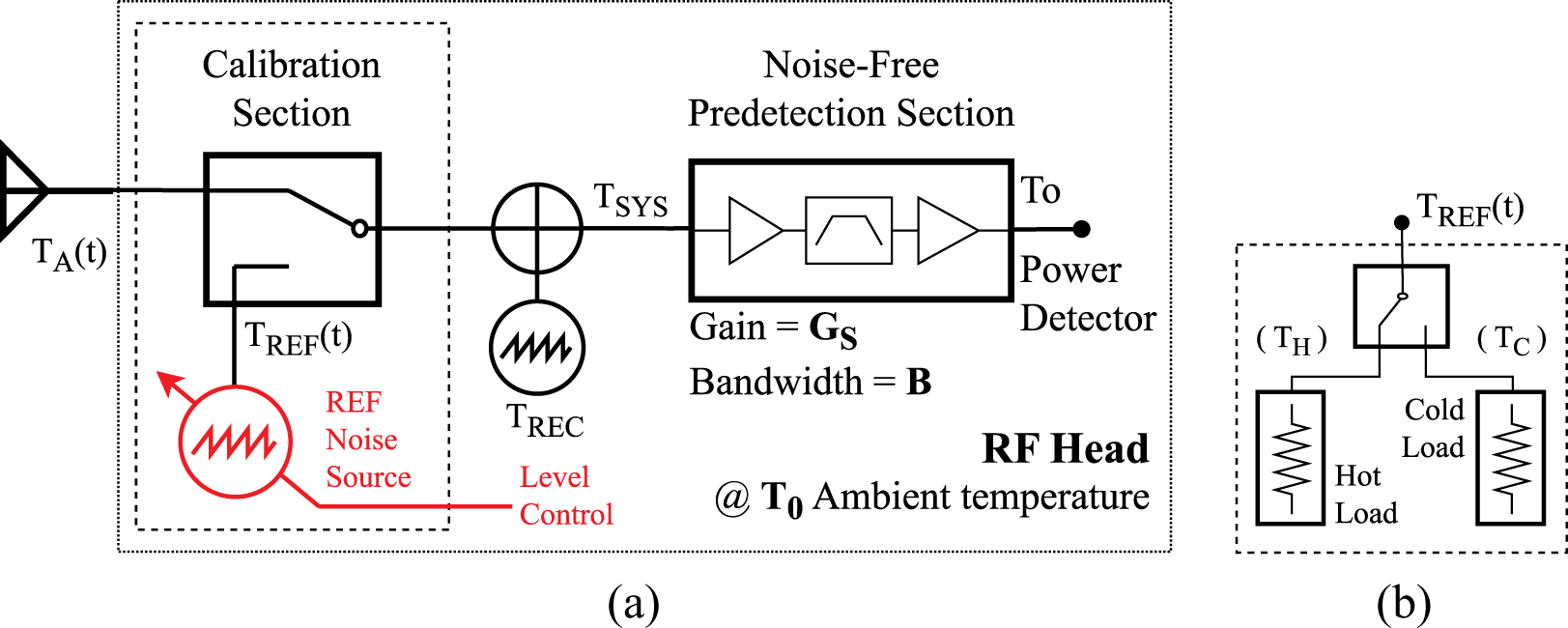
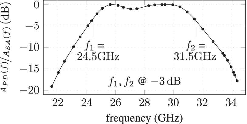


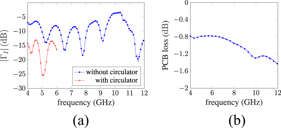
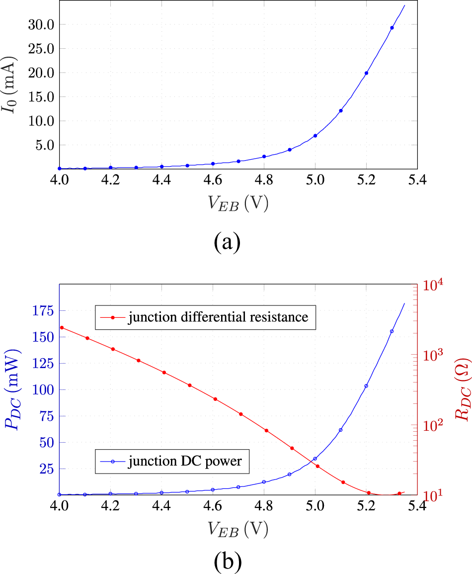
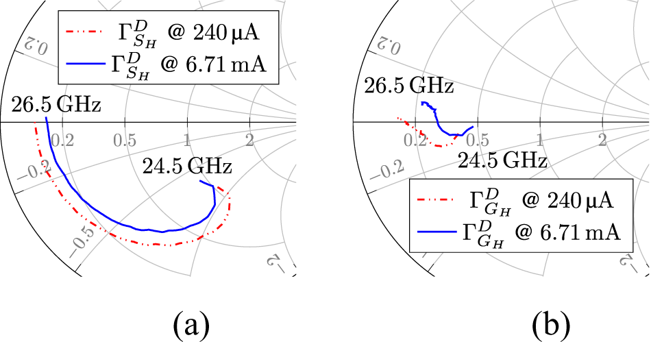


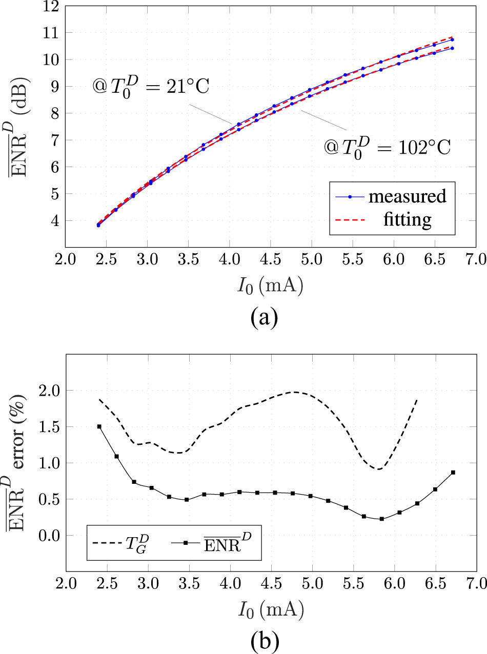


 Open access