


Introduction
The revolutionized infrastructure of the impending 5G communications networks will significantly contribute to massive advancements of telecommunication services accommodating groundbreaking applications [Reference Rost, Banchs, Berberana, Breitbach, Doll, Droste, Mannweiler, Puente, Samdanis and Sayadi1, Reference Andrews, Buzzi, Choi, Hanly, Lozano, Soong and Zhang2]. The success of these functions is feasible only through the operation in the unlicensed or lightly-licensed millimeter-wave (mm-wave) bands supporting the transmission of peak user data rates where signal up-conversion can be achieved through optical heterodyning and hybrid photonic-wireless links [Reference Rommel, Dodane, Grivas, Cimoli, Bourderionnet, Feugnet, Morales, Pikasis, Roeloffzen, van Dijk, Katsikis, Ntontin, Kritharidis, Spaleniak, Mitchell, Dubov, Carvalho and Tafur Monroy3–Reference Rommel, Thiago Raddo and Tafur Monroy6]. The convergence between optics and electronics will take place within the future 5G base stations including high speed photodiodes that convert optical signals to mm-waves and transmit them in the RF domain [Reference Konstantinou, Bressner, Rommel, Johannsen, Johansson, Ivashina, Smolders and Tafur Monroy7, Reference Perez Santacruz, Rommel, Johannsen, Jurado-Navas and Tafur Monroy8]. Among the different types of high-speed photodetectors, uni-traveling carrier photodiodes (UTC-PD) are compelling candidates for 5G applications providing increased sensitivity, broad bandwidth, and high saturation power [Reference Ishibashi and Ito9, Reference Ishibashi, Furuta, Fushimi and Ito10]. UTC-PDs are widely used in the generation of THz waves in communication and sensing applications [Reference Latzel, Pavanello, Bretin, Billet, Peytavit, Lampin, Zaknoune and Ducournau11]. For a meticulous characterization of these devices, it is essential to test properties such as responsivity measurements, 3-dB bandwidth extraction as well as saturation RF current. Moreover, the synthesis of the full equivalent circuit with lumped components based on reflection coefficients ($\Gamma$ ) is a prevalent solution for the analysis of the measured diodes [Reference Konstantinou, Caillaud, Shivan, Rommel, Johannsen, Blache, Mallecot, Krozer and Tafur Monroy12–Reference Wang, Tokumitsu, Hanawa, Yoneda, Sato and Kobayashi14]. However, the simulation of the elements composing the full equivalent is not always a feasible task. The measured reflection coefficient data of the UTC-PDs include additional information about the pads and the on-wafer transmission lines (TMLs) which are used to interconnect the intrinsic devices for probing measurements [Reference Angelini, Blache, Caillaud, Chanclou, Goix, Jorge, Mekhazni, Dupuy and Achouche15]. Even an ideal TML if not simulated accurately, may lead to a circuit that does not precisely represent the physical characteristics of the device under test (DUT). Additionally, parasitic phenomena that may occur such as signal leakage on the substrate increase the complexity of the circuit structures and impede the extraction of the values of the components synthesizing the active region of UTC-PDs. Therefore, in order to isolate these elements there are several de-embedding techniques that remove the impact of the unwanted parasitic effects added to the DUT [Reference Velayudhan, Pistono and Arnould16]. The majority of the de-embedding methods use on-wafer test structure measurements while employing analytical, algorithmic, or statistical procedures in order to retrieve the features of the DUT [Reference Cao, Zhang, Fu, Liu, Wang and Liu17–Reference Goto, Natsukari and Fujishima19]. De-embedding techniques can be classified and mathematically expressed based on lumped elements, distributed network parameters or a synthesis of the two [Reference Zhang, Xiong, Wang, Teck-Guan, Zhuang, Li and Yuan20, Reference Engen and Hoer21]. The majority of these processes require data of test structures such as short, open, and thru [Reference Bauer and Penfield22–Reference Vandamme, Schreurs and Van Dinther24]. However, there are more elaborate methods that also use on-wafer designs with various types of fabricated TMLs [Reference Zuniga-Juarez, Reynoso-Hernandez, Loo-Yau and Maya-Sanchez25–Reference Kolding28]. The choice on the number of measured structures and the total amount of de-embedding steps to perform depend on the frequency and type of the DUT [Reference Cho and Burk29–Reference Dambrine, Cappy, Heliodore and Playez31]. UTC-PDs have a single electrical port, hence open and short circuits can be used for parasitic removal [Reference Ferrero, Ghione and Pirola32].
In this study, three de-embedding techniques are analyzed (open-short, corrected, and $S$ -parameter-based) providing with a solid review of their advantages and drawbacks. This was the topic of a conference contribution at EuMW 2020 by the authors, which this paper expands upon [Reference Konstantinou, Caillaud, Rommel, Johannsen and Tafur Monroy33]. All experimental data shown are based on entirely new measurements of a more recent and upgraded generation of UTC-PDs from III-V Lab providing a substantial improvement upon the conference paper and validating the methods discussed over a larger sample of devices. Software tools and mathematical derivations are applied supporting the presented argumentation and result validity. In addition, the component estimation accuracy introduced by these methods as well as all their significant aspects are efficiently underlined. The remainder of this paper is structured as follows. Section “Physical properties and $S$
 -parameter measurements of UTC-PDs” describes the physical properties of UTC-PDs and the processes for measuring their reflection coefficients. In Section “De-embedding of UTC-PDS,” de-embedding methods utilizing open and short test structures are investigated. More specifically, the open-short technique by Koolen [Reference Koolen34], is presented and a systematic error added by the method is thoroughly examined while a correction is implemented. Furthermore, the assumptions made in order to extract the $S$
 -parameter-based technique are explained [Reference Xu and Kasper35]. In Section “Evaluating the asymmetry assumption for the TML” the impact of asymmetry affecting the TML parasitics are simulated calculating the errors acquired by applying the various techniques. Then, a comparison between all methods based on measured data is shown in Section “S-Parameter comparison between de-embedding methods.” Finally, the conclusions section summarizes the results of this study.
Physical properties and S-parameter measurements of UTC-PDs
A block diagram of the overall structure of a UTC-PD is presented in Fig. 1. The carrier generation takes place at a thin absorption layer. The holes are directly swept to the p-contact within the dielectric relaxation time of the p-doped region ($> \!{\rm THz}$ bandwidth) [Reference Ishibashi, Shimizu, Kodama, Ito, Nagatsuma and Furuta36, Reference A37]. In addition, a diffusion block layer supports the unidirectional motion of electrons toward the n-contact [Reference Zhou, Cross, Beling, Fu, Lu and Campbell38]. The speed of the device is mainly limited by the transit time of the electrons ($\tau _{tr}$
 ) within the structure. This parameter can be reduced even further once the electrons reach overshoot velocity ($v_e = 3{\rm -}5\times 10^7\, {\rm cm/s}$
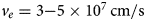 ) which depends on the length of the collector and the reverse bias ($V_{bias}$
 ) applied [Reference Thobel, Baudry, Cappy, Bourel and Fauquembergue39]. Moreover, the overshoot velocity leads to high output saturation RF currents and reduced space charge effects [Reference Preu, Dohler, Malzer, Wang and Gossard40].
UTC-PD capable of generating current at its load ($R_L$ ) due to the creation of electron-hole pairs by the absorption of photons with energy $hf$
 .
.

In order to characterize the important aspects of a UTC-PD, the extraction of the series resistance ($R_s$ ) and junction capacitance ($C_j$
 ) is crucial [Reference Riesz41]. The accumulation of the resistive effects within the doped layers of the PD can be represented by $R_s$
 . Furthermore, within the depleted active region of the device (collector), the value of $C_j$
 contributes to a thorough performance analysis of the PDs through the calculation of the bandwidth. Insight into these processes is valuable for device design, as they are used to verify that the parasitics between the designed model before and after fabrication are low. Also, it is important to mention that the junction capacitance provides information on the optimal amount of reverse bias voltage that needs to be applied in order to fully deplete the intrinsic region of the UTC-PD [Reference Li, Sun, Li, Yu, Runge, Ebert, Beling and Campbell42].
VNA measurements of UTC-PDs
Figure 2 shows a broadband, low-cost, and high-responsivity evanescent waveguide UTC-PD fabricated at III-V Lab using all 2-in InP processing including etched facet with on-wafer anti-reflection coating. The input optical waveguide can be coupled with a $3.5\, {\rm \mu } {\rm m}$ -mode diameter lensed fiber for inserting light into the UTC-PD [Reference Achouche, Magnin, Harari, Lelarge, Derouin, Jany, Carpentier, Blache and Decoster43–Reference S45]. The generated electrical signals are guided to the output through a conductor-backed coplanar waveguide (CB-CPW) where the ground pads of the CB-CPW are connected to the n-contact of the PD. Reflection coefficient measurements are conducted with the support of a probe station and a vector network analyzer (VNA). The VNA is connected to the pads of this single port device via an internal bias-tee enabling the application of reverse DC bias to the UTC-PDs. Then, the bias-tee is linked to an RF cable, and a ground-signal-ground (GSG) microwave probe [Reference Wu, Shi, Wu, Huang, Chan, Huang and Xuan46]. In order to optimize the experimental processes, VNA calibration is performed allowing the elimination of errors on the measured $S$
 -parameters that stem from the VNA and the interconnected RF components due to losses and reflections [Reference Rumiantsev and Ridler47–Reference Teppati and Ferrero49]. This procedure can be complex for optoelectronic devices due to the different nature of their ports (optical input, electrical output) [Reference Elamaran, Pollard and Iezekiel50, Reference Zhang, Zhang, Wang, Liu, Peters and Bowers51]. However, the goal of this study is the acquisition of $S_{11}$
 parameters and the electrical characterization of UTC-PDs under the dark regime where no optical illumination is applied. Thus, the calibration is conducted on a commercial wafer substrate provided by the GSG probe vendor where the standards used are open, short, and load (OSL) [Reference Chen, Wang, Liu and Zhu52]. Through the OSL correction technique of the VNA, the reference measurement plane is moved to the tip of the microwave probe [Reference Souria, Parra, Montoriol and Landez53]. All the data described are based on the same OSL calibration ensuring a fair comparison between the presented de-embedding methods. An alternative solution to the performed process is based on the replacement of the open and load with two additional offset shorts [Reference Scalzi, Slobodnik and Roberts54, Reference Cho, Kang, Lee and Koo55]. The three-offset shorts (SSS) approach is capable of achieving single port calibration on transmission media where it is difficult to realize loads or opens. It is important to note that this method is highly frequency dependent and each short should have a unique length that is precisely known and it is not proportional to multiples of $\lambda /2$
 [Reference Rytting56, Reference Hoffmann, Leuchtmann and Vahldieck57]. Once calibrated, the VNA acquires information on the reflection parameters of a PD ($\Gamma _m$
 ) that is illustrated in Fig. 3(a). $\Gamma _m$
 shows a capacitive behavior and this is confirmed by the blue curve on the Smith chart of Fig. 4 for a measured $5\times 25\, {\rm \mu } {\rm m}^2$
 UTC-PD at a reverse bias of $-2\;{\rm V}$
 . If the $S$
 -parameters of the TML $S_{TML} = [ S_{ij}] ,\; i,\; j = \{ 1,\; 2\}$
 are known, then the reflection coefficient of the active region within the UTC-PD ($\Gamma _{UTC\text {-}PD}$
 ) can be extracted analytically based on equation (1). However, the TML properties are not always easy to measure and thus de-embedding techniques are employed in order to eliminate these parasitics and move the reference measurement plane to the active region of the UTC-PDs i.e. isolate $\Gamma _{UTC\text {-}PD}$
 [Reference Zhang, Xiong, Wang, Hu and Li58]:

High-speed UTC-PD fabricated in III-V Lab connected to a VNA through an RF probe with $150\, {\rm \mu } {\rm m}$ pitch while its optical waveguide is coupled to a lensed fiber.

(a) A block diagram of the active region of an on-wafer UTC-PD connected to the waveguide pads that need to be de-embedded and (b) the short and open circuit structures.

Reflection coefficients mapped on a Smith chart for the open ($\Gamma _{OC}$ ) and short ($\Gamma _{SC}$
 ) structures as well as for a $5\times 25\, {\rm \mu } {\rm m}^2$
 UTC-PD at a reverse bias of $-2\;{\rm V}$
 .
.

Retrieving data from InP on-wafer structures with the VNA
The mathematical extraction of the $\Gamma _{UTC\text {-}PD}$ is based on the de-embedding principle that includes the measurements of the TML while it is terminated by an open (open test structure, $\Gamma _{OC}$
 ) and by a short circuit (short test structure, $\Gamma _{SC}$
 ) [Reference Velayudhan, Pistono and Arnould16]. The block diagrams of these components are depicted in Fig. 3(b). Based on the Smith chart of Fig. 4, $\Gamma _{OC}$
 (in red) has a capacitive behavior and $\Gamma _{SC}$
 (in yellow) has an inductive behavior. Both $\Gamma _{SC}$
 and $\Gamma _{OC}$
 contribute to the curvature of $\Gamma _m$
 .
.
Ideally, the retrieved reflection coefficient curves of both the short and open should coincide with the outer circle of the Smith chart where the load impedances $Z_L = 0$ and $Z_L = \infty$
 are located respectively. However, since the on-wafer components are not ideal, the measured parameters have a deviation that is also visible in the magnitude and phase of $\Gamma _{OC}$
 and $\Gamma _{SC}$
 in Fig. 5(a). Optimally, it is expected that both magnitudes to be equal to $1$
 for all frequencies. Nonetheless, losses in the conductors arise due to the finite conductivity of the metals leading to the decrease of $\vert \Gamma \vert$
 . In addition, the $\Gamma _{OC}$
 curve shows a reduction in magnitude for lower frequencies while it reverts back to higher values over 30 GHz. This may be an indication of radiation losses and parasitic coupling with neighboring on-wafer structures that are closely spaced or direct coupling between the structures and the GSG probe [Reference Phung, Schmückle and Heinrich59, Reference Schmückle, Doerner, Phung, Heinrich, Williams and Arz60]. Moreover, multiple reflections may occur before the signal reaching the end of the structure as a result of impedance mismatch between the probe tip and the on-wafer design [Reference Spirito, Gentile and Akhnoukh61–Reference Torres-Torres, Hernandez-Sosa, Romo and Sanchez63]. Another cause can be due to material characteristics as well as fabrication imperfections on the InP substrate. Thus, the representation of the TML with lumped components becomes more and more complex making the de-embedding techniques a compelling solution for extracting the active region properties.
(a) Magnitude and phase of $\Gamma _{OC}$ and $\Gamma _{SC}$
 and (b) the magnitude and phase of $\Gamma _{m}$
 for measurements of diodes with different sizes at a reverse bias of $-2\;{\rm V}$
 .
.

Figure 5(b) calculates the magnitude and phase of $\Gamma _{m}$ for UTC-PDs with different sizes at an applied bias voltage of $-2\;{\rm V}$
 . It is observed that the negative slope increases for diodes with wider surfaces. This resides on the fact that the values for the real part of the reflection coefficients ($\hbox{Re} [ \Gamma _{m}]$
 ) are higher for smaller devices due to their larger series resistance [Reference Yeganeh, Rahmatallahpur, Nozad and Mamedov64–Reference Tang, Liu, Wang and Wang66]. Moreover, the imaginary part of the $\Gamma _{m}$
 values ($\hbox{Im}[ \Gamma _{m}]$
 ) also show the same trend where the capacitive behavior of the active region is more dominant for wider structures comparing to the parasitics of the TML [Reference Wang, Pan, Tang and Liu67–Reference Doussin, Bajon, Wane, Magnan and Parra69]. The opposite occurs for small diodes (e.g. $4\times 10\, {\rm \mu } {\rm m}^2$
 ) where the TML principally influences the magnitude and phase of $\Gamma _m$
 that is equal to $\sqrt {( \hbox{Re}[ \Gamma _{m}] ) ^2 + ( \hbox{Im}[ \Gamma _{m}] ) ^2}\angle ( \hbox{Re}[ \Gamma _{m}] ,\; \hbox{Im}[ \Gamma _{m}] )$
 .
.
De-embedding of UTC-PDs
The valuable information extracted for $\Gamma _{OC}$ , $\Gamma _{SC}$
 , and $\Gamma _{m}$
 are inserted to de-embedding equations calculating the reflection coefficient of the PDs’ $\Gamma _{UTC\text {-}PD}$
 . At a further step, $\Gamma _{UTC\text {-}PD}$
 is introduced to a software-based circuit model where the active region of the diodes can be simulated as the RC circuit shown in Fig. 6(a) [Reference Mukherjee, Mounaix, Maneux, Natrella, Seddon, Graham and Renaud70]. It is worth noting that a leakage branch including a capacitor in series with a resistor can be added in parallel to $C_j$
 [Reference Matters-Kammerer, Tripodi, van Langevelde, Cumana and Jansen71, Reference Tang, Drakinskiy, Yhland, Stenarson, Bryllert and Stake72]. This part is not removed from the de-embedding but due to its high impedance is considered as open and can be omitted without an impact on the measured data [Reference Anagnosti, Caillaud, Paret, Pommereau, Glastre, Blache and Achouche73]. The lumped elements for $C_j$
 and $R_s$
 are obtained by using the optimization feature of the software that is capable of minimizing the error difference ($\epsilon$
 ) between the extracted data i.e. $\Gamma _{UTC\text {-}PD}$
 and the reflection coefficient of the circuit model ($\Gamma _{model}$
 ) where $\epsilon = \vert \Gamma _{UTC\text {-}PD}-\Gamma _{model}\vert /\vert \Gamma _{UTC\text {-}PD}\vert$
 [Reference Marques da Costa, Kurokawa, do Prado and Pissolato74].
(a) Circuit model for the measurements of the UTC-PDs showing the point of the measured reflection coefficient $\Gamma _{m}$ and the displacement of the reference plane to the active region of the diodes after implementing the de-embedding equations that lead to the removal of the TML parasitics ($S_{TML}$
 ) and (b) two representations of the TML based on the Pi lumped equivalent model and the distributed model.

The open-short de-embedding
The open-short method introduced by Koolen [Reference Koolen34] is based on the conversion of all measured $S$ -parameters into admittances ($Y$
 ) and calculates the impedance of a DUT by implementing equation (2) [Reference Tiemeijer, Pijper and van der Heijden75]:

This technique is applied to a $5\times 25\, {\rm \mu } {\rm m}^2$ UTC-PD and the Smith chart of Fig. 7(a) is obtained. It is evident that the de-embedded (red) curve of $\Gamma _{Koolen}$
 has also a capacitive behavior while the parasitics introduced by the waveguide are removed. The differences between the two reflection coefficients are also calculated in Fig. 7(b) based on magnitude and phase. As previously stated, the added parasitics from the TML increase the negative slope of the $\Gamma _{m}$
 comparing to the de-embedded $\Gamma _{Koolen}$
 .
.
(a) Impact of the open-short method on a $5\times 25\, {\rm \mu } {\rm m}^2$ UTC-PD leading to the removal of the waveguide parasitics at $-2\;{\rm V}$
 reverse bias plotted on a Smith chart and (b) the magnitude and phase of $\Gamma _{m}$
 and $\Gamma _{Koolen}$
 .
.

With regard to the lumped equivalent circuit of the active region, it is expected that $Z_{Koolen} = Z_{UTC\text {-}PD}$ . However, in order to acquire a perfect optimization in the circuit simulations software and minimize $\epsilon$
 , an inductor ($L_p$
 ) needs to be added in series with the $Z_{UTC\text {-}PD}$
 of Fig. 6(a) after the TML. This additional element contradicts with the predicted circuit model of the active area within a PD [Reference Lucovsky, Lasser and Emmons76]. The origin of $L_p$
 is thoroughly analyzed in the following section.
Analysis of the inaccuracies introduced by the open-short method
In order to verify the existence and magnitude of the additional inductance, the open-short de-embedding is investigated analytically. As depicted in Fig. 6(b), the TML connected to the DUT can be based on the distributed model. The transfer matrix for this type of ideal waveguide with length $l$ is given by equation (3), with a propagation constant $\gamma = \sqrt {zy}$
 and $z = R + j\omega L\approx j\omega L$
 , y = jωC [Reference Cortés-Hernández, Sánchez-Mesa, Sejas-García and Torres-Torres77]. Finally, $Z_c = \sqrt {z/y}$
 is the characteristic impedance of the line. Each variable is measured in units per transmission length:

By converting the impedances of this symmetric model ($S_{11} = S_{22}$ ) in equation (3) to admittances through inversion and replacing them into the equation (2) result in:

The term $\cosh ^2( \gamma l)$ can be approximated with a Taylor series and thus,

is extracted. The residual error ($R_2$ ) for this Taylor approximation is presented in equation (6). It is a constant that multiplied by an impedance results in negligible values and therefore can be omitted:

If the DUT is a UTC-PD i.e. $Z_{UTC\text {-}PD} = R_s-j( {1}/{\omega C_j})$ , and by replacing it in equation (5), then,

is obtained. Consequently, equation (7) agrees with the previous statement that $Z_{Koolen}\neq Z_{UTC\text {-}PD}$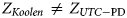 for both the real and imaginary parts of the UTC-PD. For low frequencies, the real parasitic term $\vert R_s( \gamma l) ^2\vert = \vert R_s\omega ^2LCl^2\vert$
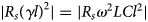 that depends on the characteristics of the TML ($L,\; C,\; l$
 ) can be omitted ($< 1\!{\rm m\Omega }$
 ). However, in higher frequencies its quadratic impact increases reducing the series resistance. The additional inductance ($L_p = ( {LC}/{C_j}) l^2$
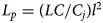 ) that is calculated it is inversely proportional to the junction capacitance of the device. The exact same result for $L_p$
 is measured if the equation of the open-short method is implemented to the Pi and T equivalent models of a waveguide [Reference Pozar78]. Based on this process it is proven that a systematic error is added to $Z_{DUT}$
 while using the Koolen de-embedding technique. In principle, since the device model of Fig. 6(a) is related to different types of diodes such as PN, PIN, and Schottky, it is expected that the same error would occur once the open-short technique is applied [Reference Alamoud, Al-Mashary and Ragaie79–Reference Semple, Georgiadou, Wyatt-Moon, Gelinck and Anthopoulos81].
These analytical calculations concerning the additional inductance are confirmed through circuit simulations based on experimental data for diodes with different reverse bias applied, sizes, and frequency of operation. In theory, the value of $C_{j_{th}} = \epsilon A_j/l_j$ is proportional to the junction area ($A_j$
 ) and inversely proportional to the junction length that is directly linked to the reverse bias. In the case where the bias is not enough to fully deplete the active region of a UTC-PD leads to a decrease of $l_j$
 increasing $C_j$
 . In addition, the deteriorating junction area of a PD reduces the value of $C_j$
 while $L_p$
 increases. In Fig. 8, the junction capacitance and inductance of a $5\times 25\, {\rm \mu } {\rm m}^2$
 UTC-PD is extracted for different values of the reverse bias. As expected, the form of the curve of $C_j$
 (blue) is approximately a reflection of $L_p$
 (red) as a reference to the $x$
 -axis, verifying the previous observations on the inverse proportional relationship between these two lumped components.
Descending behavior of the additional inductance ($L_p$ ) extracted from the open-short method as a function of the applied reverse bias that is inverse to the curve for the junction capacitance.

Furthermore, in the ideal case, the values of the junction capacitance are expected to be constant as a function of frequency. However, since $C_j$ is extracted based on $S$
 -parameter measurements it is expected to show a small deviation for different frequencies with $C_j$
 being higher at low frequencies due to parasitic effects [Reference Natrella, Liu, Graham, van Dijk, Liu, Renaud and Seeds82]. This deviation (in percentages) is depicted in Fig. 9(a) where for the same diodes, the junction capacitance calculated over the range 0–$35\, {\rm GHz}$
 shows higher values comparing to the data measured between 0 and 50 GHz. The maximum percentage of difference at $1.65\%$
 is obtained for a diode with size of $4\times 15\, {\rm \mu } {\rm m}^2$
 . This directly affects the calculation of $L_p$
 that is plotted in Fig. 9(b) as a function of increasing $A_j$
 for different measured UTC-PDs at a bias of $-2\;{\rm V}$
 . Then, a hyperbolic curve fitting is used in order to show the inverse proportionality of $L_p$
 to the sizes of the diodes while $LCl^2$
 is constant. As previously discussed, this curve is shifted upward for higher frequencies.
(a) Percentage of difference between the values of $C_j$ extracted up to $35$
 and $50\;{\rm GHz}$
 affecting the calculation of $L_p$
 and (b) the additional inductance ($L_p$
 ) introduced by the open-short technique as a function of area at a reverse bias voltage of $-2\;{\rm V}$
 for different UTC-PDs up to $35$
 and $50\, {\rm GHz}$
 .
.

A correction to the open-short method
To eliminate the additional inductive behavior of equation (7), a correction to the open-short technique needs to be introduced, isolating $Z_{UTC\text {-}PD}$ . Therefore, the term $\cosh ^2( \gamma l)$
 in (4) is expressed as a function of the two known variables imported from the open ($Y_{OC}$
 ) and short ($Y_{SC}$
 ) structures:

Calculating $Y_{OC} + Y_{SC}$ in equation (8), as well as taking into account $\cosh ^2( \gamma l) + \sinh ^2( \gamma l) = 2\cosh ^2( \gamma l) -1$
 of the hyperbolic trigonometric identities and equation (4), results in equation (9) which introduces a correction forming an impedance-based de-embedding capable of removing the systematic error imported in equation (2) for any single-port-based DUT:

The de-embedded reflection coefficients based on the open-short technique and its correction are calculated and plotted in the Smith chart of Fig. 10(a) for the same $5\times 25\, {\rm \mu } {\rm m}^2$ . The curves for $\Gamma _{Koolen}$
 and $\Gamma _{Corrected}$
 overlap while the one for the open-short is longer due to $L_p$
 added by the method itself. A similar observation can be extracted from Fig. 10(b) where the magnitude and phase of the two obtained reflection coefficients are plotted. Consequently, equation (9) is capable of isolating the active region of a UTC-PD leading to the valid design of its circuit model matching the impedance $Z_{UTC\text {-}PD}$
 and can be expanded to all devices using open and short structures for de-embedding.
(a) Impact of the corrected method to a $5\times 25\, {\rm \mu } {\rm m}^2$ UTC-PD leading to the removal of the waveguide parasitics at $-2\;{\rm V}$
 reverse bias depicted on a Smith chart; the corrected curve is compared to $\Gamma _{Koolen}$
 showing the additional inductance $L_p$
 and (b) the magnitude and phase of $\Gamma _{Koolen}$
 and $\Gamma _{Corrected}$
 .
.

The $S$ -parameter-based de-embedding method

An alternative process that can be implemented in order to de-embed the parasitics of the UTC-PDs is the $S$ -parameter-based (SPb) method. This mathematical approach resides on primarily reducing the unknown $S$
 -parameter variables of the TML ($S_{TML}$
 ) in equation (1) from four to two. This is initially accomplished by implementing the property of passive behavior of the TML connected to the UTC-PD where $S_{12} = S_{21}$
 . Moreover, by assuming the symmetry of the TML, the equality between $S_{11}$
 and $S_{22}$
 is acquired. The validity of this hypothesis is substantial and it will be investigated even further through simulation processes in the following section. The de-embedding equation is finally derived in equation (10) as a function of $\Gamma _{m},\; \Gamma _{OC}$
 and $\Gamma _{SC}$
 by replacing and rearranging the variables in equation (1) from the data obtained for the open structure, $\Gamma _{DUT} = 1,\; \Gamma _{m} = \Gamma _{OC}$
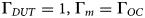 and for the short $\Gamma _{DUT} = -1,\; \Gamma _{m} = \Gamma _{SC}$
 . The Smith chart of Figs 11(a) and (b) presents the impact of the $S$
 -parameter-based method on a $5\times 25\, {\rm \mu } {\rm m}^2$
 UTC-PD where the TML parasitics are removed in the curve of $\Gamma _{SPb}$
 :
:

(a) Impact of the $S$ -parameter-based method to a $5\times 25\, {\rm \mu } {\rm m}^2$
 UTC-PD leading to the removal of the waveguide parasitics at $-2\;{\rm V}$
 reverse bias mapped on a Smith chart and (b) the magnitude and phase of $\Gamma _{SPb}$
 and $\Gamma _{m}$
 .
.

Evaluating the asymmetry assumption for the TML
The error estimation that is introduced due to the asymmetry assumption of the TML connected to the DUT is essential to be extracted in order to calculate the errors that are introduced in the de-embedding processes. This is achieved through the simulation where a PD is connected to a TML that is based on the Pi-model of Fig. 6(b) and is designed with lumped components ($C_{TML_1} = 21.3\, {\rm fF}$ , $L_{TML} = 55.6\, {\rm pH}$
 , $R_{TML} = 0.3\, {\rm \Omega }$
 ). The TML of the circuit exhibits $100\%$
 of symmetry if $C_{TML_1} = C_{TML_2}$
 , i.e. $S_{11} = S_{22}$
 . Asymmetry can be introduced by setting $C_{TML_2} = ( 1-a) C_{TML_1}$
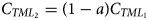 where $a$
 is a scaling factor varying between $0$
 and $1$
 where $1$
 represents a fully asymmetric ($100\%$
 ) TML. The values of the lumped components for these simulations are chosen based on measurements of $5\times 25\, {\rm \mu } {\rm m}^2$
 UTC-PD ($C_{j} = 37.7\, {\rm fF}$
 , $R_{s} = 14.9,\; {\Omega }$
 ). The circuit simulator is used to calculate the $S_{TML}$
 as well as the reflection coefficients of the TML while it is terminated by a short ($\Gamma _{SC}$
 ) and by an open circuit ($\Gamma _{OC}$
 ) reproducing the test structures on a real wafer for frequencies up to $50\, {\rm GHz}$
 . The first figure of merit that is tested is the effect of the asymmetry on the $S_{11}$
 and $S_{22}$
 parameters of the TML. Therefore, $\Delta S_{TML} = \vert S_{11}-S_{22}\vert /S_{11}$
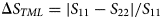 is introduced comparing the magnitude of the reflection coefficient $S_{11}$
 to $S_{22}$
 [Reference Xu and Gao83]. The $\Delta S_{TML}$
 is calculated for an ascending value of the asymmetry factor $a$
 . The results are provided in Fig. 12 where it is evident that the asymmetry of a TML affects its $S$
 -parameters. At a further step, the impact of increasing $a$
 is implemented in order to investigate its effect on the de-embedding equations (2), (9), and (10).
$\Delta S_{TML}$ as a function of frequency for different asymmetry values.

Asymmetry dependence in $S$-parameter-based method

Figure 13 examines the percentage of difference between the junction capacitance and series resistance extracted in both equation (1) that provides the exact values of $C_j$ and $R_s$
 and the resulting lumped elements calculated by equation (10) as a function of the increasing asymmetry. The curves are linear and maximum difference reaches $7.1\%$
 for $C_j$
 and $8.2\%$
 for $R_s$
 once $a = 1$
 . Similar behavior is demonstrated in the percentage differences in the mean values of magnitude, phase, real and imaginary parts of the diode's reflection coefficients ($\Gamma _{UTC\text {-}PD}$
 ).
).
Percentage difference of $C_j$ , $R_s$
 , and of the characteristic properties of $\Gamma _{UTC\text {-}PD}$
 between the $S$
 -parameter-based and direct methods as a function of the increasing TML asymmetry.

Thus, the extracted data confirm that the TML symmetry influences the $S$ -parameters ($\Gamma _{SPb}$
 ) of the de-embedded circuits as well as the values of the lumped components $C_j$
 and $R_s$
 . However, the percentage of difference does not exceed the $8.2\%$
 for all the tested variables while the performance of the technique improves while the additional branch is added on the TML. Identical values are observed once the equation for the corrected method ($Z_{Corrected}$
 ) is used. Since there is not an effective divergence between the de-embedded elements and the original data, the $S$
 -parameter-based method can be considered as an alternative de-embedding leading to the removal of the TML parasitics from a DUT.
Asymmetry dependence in open-short method
Similar procedure is applied while implementing the open-short de-embedding in order to analyze the impact of asymmetry. The results of this procedure are shown in Fig. 14 for the series resistance, junction capacitance, and additional inductance.
Percentage difference of $C_j$ , $R_s$
 , and $L_p$
 between the open-short and direct methods as a function of the increasing TML asymmetry.

While the percentage of difference on the extraction of $C_j$ is low varying between $-0.33$
 and $0.21\%$
 , the real part of the intrinsic region ($Re[ Z_{UTC\text {-}PD}]$
 ) is directly affected by the type of the TML linked to the active area of the UTC-PD. The value for $Rs$
 is $19.1\%$
 lower than the actual once the $C_{TML_2}$
 rises. This percentage is linearly reducing for increasing $a$
 due to the decrease of the factor $LC$
 in the real part of equation (7). The same trend is presented for the value of $L_p$
 .
.
These results show that the open-short technique is capable of successfully removing the TML parasitics. However, once a second parallel branch with increasing admittance is shunt in the line model, the process starts demonstrating errors that become significant for low $a$ . It is important to underline that the increasing $L_p$
 for high values of $C_{TML_2}$
 can be a good indication on the type of TML that is experimentally measured as well as on the effectiveness of the open-short especially for the calculation of $R_s$
 . Therefore, the additional inductance is not only dependent on the diode size, reverse bias voltage applied, and the frequency of operation (Figs 8 and 9(b)) but also on the type of the TML. Finally, this simulation validates the mathematical analysis of equation (7) on this series component i.e. $L_p$
 added by the process.
S-Parameter comparison between de-embedding methods
Section “Evaluating the asymmetry assumption for the TML” provides with a good insight into the behavior of the de-embedding techniques based on circuit simulation level. However, it is of the essence to compare the discussed techniques on their analytical equations and their impact on the measured de-embedded lumped equivalent data.
Comparison $S$-parameter-based – corrected

In order to compare the de-embedding methods for the corrected and $S$ -parameter-based technique the de-embedded $S$
 -parameters for $\Gamma _{Corrected}$
 and $\Gamma _{SPb}$
 of Figs 7 and 11 respectively are superimposed on a Smith chart leading to an overlap between the two red curves. Moreover, the error difference between the magnitudes of the two reflection coefficients is negligible. That is due to the fact that both the techniques in equations (9) and (10) are extracted based on the symmetry of the TMLs. With further mathematical analysis the conversion equation from $Z$
 to $S$
 parameters in equation (11) [Reference Frickey84] is implemented:

By substituting equations (11) to (9) then,

is obtained.
If equation (12) is rearranged and $\Gamma _{Corrected}$ is extracted, the corrected method becomes identical to the $S$
 -parameter-based ($\Gamma _{Corrected} = \Gamma _{SPb}$
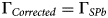 ). Therefore, the two de-embedding processes converge and both $Z$
 and $S$
 parameters can be used to calculate a valid equivalent for the active area of UTC-PDs.
Comparison Koolen – corrected
A similar process is conducted for the comparison between the open-short and the corrected method. As a first step, equation (2) is analyzed based on $Z$ -parameters in equation (13):

Then, the error ratio of difference between $Z_{Koolen}$ and $Z_{Corrected}$
 is expressed in equation (14) as a function of $Z_{OC}$
 and $Z_{SC}$
 :
:

In the ideal case where the ratio is a real number, i.e. $\beta = 0$ the relationship between the lumped elements for $R_s$
 and $C_j$
 extracted by the two methods is given in equation (15):

For the two techniques, both $R_s$ and $C_j$
 are dependent on the propagation constant of the waveguide ($\gamma$
 ) with $C_{j, Koolen}> C_{j, Corrected}$
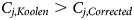 and $R_{s, Koolen}< R_{s, Corrected}$
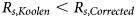 . However, the measurement results contradict with the ideal scenario since it is calculated that $R_{s, Koolen}> R_{s, Corrected}$
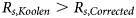 clarifying that it is important to take into account the impact of the imaginary part of equation (14), i.e. $\beta \neq 0$
 . This is because, as shown in Figs 4 and 5(a), the open and short circuit curves are not ideal. Therefore, by taking into account that the product $\beta \omega R_{s, Corrected} C_{j, Corrected}\approx 10^{-6}$
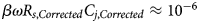 the results of equation (16) are obtained:

The analysis above confirms that the relationship of $R_s$ and $C_j$
 between the two methods is more complex and it depends on both $a( \omega )$
 and $\rho ( \omega ,\; C_j)$
 that includes the parameter $\beta$
 and the $C_{j, Corrected}$
 that is directly connected to the UTC-PD's area ($A_j$
 ). In Fig. 15(a), the factors $\alpha ( \omega )$
 and $\rho ( \omega ,\; C_j)$
 are plotted as a function of frequency showing that $a( \omega )$
 decreases at higher frequencies while the opposite occurs to $\rho ( \omega ,\; C_j)$
 . In order to get a better perspective on the impact of the different PD sizes to the magnitude of these factors, averaging over frequency is implemented removing $\omega$
 from the variables of freedom in $\alpha$
 and $\rho$
 . Thus, $a( \omega )$
 as well as each curve of $\rho ( \omega ,\; C_j)$
 is represented by a single value. Figure 15(b) shows that ${\alpha }$
 remains constant as a function of increasing $C_j$
 while ${\rho }( C_j)$
 decreases exponentially. Therefore, based on the calculated data it is expected that $C_{j, Koolen}\approx C_{j, Corrected}$
 while $R_{s, Koolen}> R_{s, Corrected}$
 since the impact of the of ${\rho }$
 is high especially for smaller junctions.
(a) $\alpha ( \omega )$ and $\rho ( \omega )$
 as a function of increasing frequency for different diode capacitances and (b) ${\alpha }$
 and ${\rho }$
 as a function of $C_j$
 .
.

These characteristics are verified in Fig. 16 where the percentage of difference between the lumped components of the active region ($C_j,\; R_s$ ) for the open-short and the corrected method are plotted using real measurements for diodes with different sizes. The percentage of error difference between $C_{j, Koolen}$
 and $C_{j, Corrected}$
 increases as a function of size not exceeding the absolute value of $1.8\%$
 . The negative percentage implies that in the corresponding junction area, the lumped element has higher magnitude once it is obtained by the corrected method. Concerning the series resistance, the difference between the two methods starts with a significant difference of $15.2\%$
 and decreases to values of approximately $1.6\%$
 for high size devices such as a $6\times 50\, {\rm \mu } {\rm m}^2$
 UTC-PD.
Percentage of difference of the lumped element components between the open-short and corrected methods.

The extracted data of these elements are also shown in Fig. 17 for the different de-embedding techniques. Furthermore, the theoretical curve of the junction capacitance ($C_{j_{th}}$ ) is also calculated. It can be observed that for all the different junction areas, the theoretical curve is shifted downward by a constant equal to $5\, {\rm fF}$
 . The difference between the dotted line for $C_{j_{th}}$
 and the actual measurement data can be caused due to a parasitic capacitance generated by leakage of electric field at the edges of the diodes’ intrinsic region toward the neighboring layers of the collector layer forming a fringe capacitor in parallel to $C_j$
 [Reference Chuang, Wang, Chu, Chang and Hu85–Reference Yu, Sun, Yu and Beling87]. In summary, the classical method of open-short provides both the $R_s$
 and $C_j$
 at the price of adding a virtual inductance ($L_p$
 ) with reduced values for $R_s$
 in high frequencies leading to an imprecise circuit model of the intrinsic area within the photodetectors. This error is fixed by using an updated method (corrected) and its equivalent $S$
 -parameter-based technique. The difference between these three methods in terms of the accuracy of the equivalent circuit and its component magnitudes are mainly based on the assumptions made for the equation calculations, the TML characteristics, the frequency of operation as well as the quality and precision of the on-wafer measurements conducted with the VNA [Reference Khelifi, Reveyrand, Lintignat, Jarry, Quéré, Lapierre, Armengaud and Langrez88]. Overall, the use of these de-embedding methods provides with a good estimation for the values of the lumped elements within the active region of the diodes that are a valuable tool for the characterization and analysis of their physical properties.
Impact of the corrected method to a $5\times 25\, {\rm \mu } {\rm m}^2$ UTC-PD leading to the removal of the waveguide parasitics at $-2\;{\rm V}$
 reverse bias.

Conclusion
Within the base stations of the future 5G wireless communication networks, UTC-PDs will play a crucial role in interfacing the optical domain of passive optical networks and the mm-wave generation, due to their low-cost, broad bandwidth, and high saturation RF currents. UTC-PDs integrated with high-speed electronics will offer a compelling solution supporting the huge amount of 5G end-users. The design of such complex systems requires an accurate knowledge of the equivalent circuit of UTC-PDs and especially their active region. Such process will provide with a good overview on the bandwidth and the output powers of the generated signals that flow toward the radiating mm-wave antennas. However, the complex nature of the electrical TMLs linked to the diodes do not allow their simulation with lumped elements leading to the implementation of mathematical de-embedding equations. This paper summarizes and compares de-embedding techniques that focus on the importance of removing the parasitic effects added by the waveguides and are capable of extracting the junction capacitance and series resistance of UTC-PDs, as well as verifies them with a set of devices designed and fabricated at III-V Lab. The open-short and the $S$ -parameter-based de-embedding techniques are applied on experimental data leading to circuit simulations. It is observed that a systematic error is added by the open-short method that was thoroughly studied and it is highly dependent on the diodes’ reverse bias, the frequency of operation, and the complexity of the TML parasitics. The mathematical removal of this error led to the derivation of an updated equation that eliminates its impact. Moreover, the assumptions made in defining the $S$
 -parameter-based equation are tested by simulations calculating the significance of these assumptions. Satisfactory results were provided since minimal error is introduced. A thorough comparison between these methods led to the convergence of the corrected with the $S$
 -parameter-based method. As a result, the error of difference between the experimentally extracted $C_j$
 and $R_s$
 for all techniques is not high making them reliable candidates for the calculation of the characteristic features of the UTC-PDs. Finally, the improvement upon the de-embedding techniques that is proposed with the corrected method minimizes the inaccuracies introduced in the circuit modeling.
Acknowledgement
This study was partially funded by the 5G STEP FWD, 5G-PHOS and blueSPACE projects with funding from the European Union's Horizon 2020 research and innovation program under grant agreement numbers 722429, 761989, and 762055, respectively.
 Dimitrios Konstantinou received his Diploma in Electrical and Computer Engineering from the National Technical University of Athens, in 2015. He finished his Master studies in Telecommunications with a specialty at the Technical University of Denmark in 2017. Since October 2017 he is a doctorate candidate at the Eindhoven University of Technology (TU/e). He is part of the ITN European Project 5G STEP FWD with focus on the synthesis of High Speed 5G Base Stations combining Photonic and Electronic Integration on InP.
 Christophe Caillaud received the engineering degree from ESPCI and the master’s degree from Ecole Polytechnique in 2007. He then received the Ph.D. degree from Ecole Nationale Supérieure de Télécommunications de Paris in 2010, working on the integration of high-speed photodiodes with semiconductor optical amplifiers. He was then hired by Alcatel-Lucent (now part of Nokia) and works on high-speed III-V photonic integrated circuits within III-V Lab, a joint venture between Nokia Bell Labs, Thales, and the CEA Leti.
 Simon Rommel obtained his B.Sc. from the University of Stuttgart, Germany in 2011 and, in 2014 obtained his M.Sc. degrees in Photonic Networks Engineering from Aston University, Birmingham, UK and Scuola Superiore Sant'Anna, Pisa, Italy. He completed his Ph.D. in 2017 at the Technical University of Denmark, Kongens Lyngby, Denmark with research focused on photonic-wireless convergence and millimeter-wave radio-over-fiber links. In 2017 he visited the National Institute of Information and Communications Technology, Koganei, Tokyo, Japan for a research stay. Since 2017 he is with Eindhoven University of Technology as a postdoctoral researcher, continuing his work on photonic and radio frequency technologies with a strong focus on implementations for 5G. His research interests include the fields of fiber-optic and wireless communications and the associated digital signal processing. He has contributed to multiple national and European research projects, incl. H2020 blueSPACE as technical manager. Dr. Rommel is a member of IEEE, OSA, IET, and VDE.
 Ulf Johannsen obtained his Dipl.-Ing. degree from the Hamburg University of Technology, Germany, in 2009 and his Ph.D. degree from the Eindhoven University of Technology (TU/e), the Netherlands, in 2013. In the same year he started as Senior Systems Engineer at ATLAS ELEKTRONIK GmbH in Bremen, Germany. Here, he worked as system designer and engineering manager on autonomous underwater vehicle (AUV) systems with sonar payloads. His responsibilities included the specification and architecting of the entire systems as well as the lead of multi-disciplinary development teams in order to meet those specifications within time and budget. Since 2016 he is assistant professor with the Electromagnetics group at TU/e. His research focus lies on (sub-)millimeter-wave antenna systems for various applications. Moreover, he leads the Ultra-High-Data-Rate program within TU/e's Centre for Wireless Technology. Dr. Johannsen is the chairperson of the IEEE Benelux joint AP/MTT chapter.
 Idelfonso Tafur Monroy graduated from the Bonch-Bruevitch Institute of Communications, St. Petersburg, Russia, in 1992, where he received his M.Sc. degree in multichannel telecommunications. In 1996, he received a Technology Licentiate in telecommunications theory from the Royal Institute of Technology, Stockholm, Sweden. In the same year, he joined the Electrical Engineering Department, Eindhoven University of Technology, the Netherlands, where he received his Ph.D. degree in 1999 and worked as an Assistant Professor until 2006. He founded in 2008 and led until 2017 the Metro Access and Short Range Communications Group of the Department of Photonics Engineering, Technical University of Denmark. He currently is affiliated with the Electrical Engineering Faculty at TU/e. He participated in several European research framework projects in photonic technologies and their applications to communication systems and networks. His research interests include terahertz wireless communication and sensing systems, quantum secure digital infrastructures, and application of nanophotonic technologies in communications and security.


 Open access