

Introduction
Complex oxide heterostructures have generated tremendous research interest[ Reference Hwang, Iwasa, Kawasaki, Keimer, Nagaosa and Tokura 1 – Reference Habermeier 3 ] due to the wealth of new physical properties needed for solid-state devices with novel functionalities unattainable with conventional semiconductor structures. In particular, ferromagnetic oxides, superconductors, multiferroics, and other multifunctional oxide materials offer rich possibilities for exploration of both fundamental physical phenomena and device applications. With the advancements in the growth of epitaxy oxide materials, epitaxial oxide heterostructures are emerging as outstanding candidates for realization of devices in which diverse material properties such as ferromagnetism, ionic conductivity, piezoelectricity, and ferroelectricity can be flexibly coupled to achieve new functionality.
However, putting this functionality to work remains a key issue. To date, most of the works reported[ Reference Hwang, Iwasa, Kawasaki, Keimer, Nagaosa and Tokura 1 – Reference Habermeier 3 ] in the literature have dealt with heterostructures grown on closely lattice-matched insulating substrates such as DyScO3 (DSO), NdGaO3 (NGO), SrTiO3 (STO), and molecular beam epitaxy (MBE)-grown STO-buffered Si (100). However, the small (1%–2%) strain in the resulting heterostructures is difficult to relax because of finite critical thickness considerations and associated difficulties related to dislocation nucleation and glide to the interface. These layers contain unrelaxed strains, which can lead to formation of point defects and long-term degradation of the physical properties, thus adversely affecting the device characteristics. In addition, most of the above substrates are incompatible with existing CMOS-based technology based on Si (100).
Hence, in order to explore the potential applications of these oxide materials in memory and microelectronic devices, the integration of their functionality on Si (100) is required. Integration of crystalline oxides on a silicon (Si) platform circumvents the need of growing larger diameter ceramic substrates typically used to grow oxide heterostructures. Furthermore, their integration on Si offers significant advantages in terms of heat dissipation for potential power applications, since the thermal conductivity of Si is an order of magnitude higher than that of typical oxide substrates. Hence, to fully exploit the functionalities of the perovksite oxides in device applications, one must be able to grow these heterostructures on Si (100).
LCMO is a conducting double exchange ferromagnetic metallic oxide[ Reference Ramirez 4 , Reference Salamon and Jaime 5 ] at T C ~ 230–250 K with a spin-only magnetic moment of 3–3.7 µB. Among the transition metal oxides, SrRuO3 (SRO) is unique in that it is a 4d transition metal oxide that exhibits ferromagnetism and metallic conductivity,[ Reference Gan, Rao, Eom, Garrett and Lee 6 ] with a moment of 1.1–1.6 µB per Ru4+ ion. SRO is a good candidate for the biasing layer due to its large anisotropy and large coercive field (H c). The T C of SRO is near 160 K. It is also a routinely used electrode material to fabricate capacitor structures using ferroelectric oxides. Both these oxides have high chemical stability, and good thermal properties. Most importantly, the similar perovskite crystal structure of these two oxides facilitates the easy integration with other oxide materials to form heterostructures.
To date, studies in the literature have focused on the rich physics found at the La0.7Sr0.3MnO3 (LSMO)/SRO interface. In these heterostructures interesting magnetic properties such as antiferromagnetic exchange coupling and its cross-over to ferromagnetic exchange coupling[ Reference Ke, Rzchowski, Belenky and Eom 7 – Reference Singamaneni, Prater and Narayan 11 ] have been identified. Despite the fact that La0.7Ca0.3MnO3 (LCMO) shares similar electronic and magnetic properties with LSMO, there has been no report on the epitaxial growth and investigation of magnetic properties of LCMO when it is interfaced with SRO layer on any substrate. In this paper, we demonstrate the epitaxial integration of LCMO/SRO on Si (100) by means of pulsed laser deposition (PLD) using domain matching epitaxy (DME) paradigm, which involves matching of integral multiples of lattice planes across the film–substrate interface,[ Reference Narayan 12 , Reference Narayan and Larson 13 ] that can accommodate the growth of heterostructures with lattice misfit strain in excess of 30%. The present work shows that these heterostructures are strain relaxed as each layer grew cube-on-cube, and LCMO and SRO layers retain their respective bulk magnetic properties such as coercive field and Curie temperature.
Experimental details
A Lambda Physik (LPX200) pulsed KrF excimer laser beam (wavelength λ = 248 nm, pulse width τ = 25 ns, and repetition rate 5–10 Hz) is incident on the target at an angle close to 45° with a spot size about 1 × 4 mm2. The distance between the target and the substrate was maintained at 45–50 mm. We have used the energy density and pulse frequency as 1.5–3 J/cm2 and 10 Hz, respectively. Prior to the deposition, the chamber was evacuated to a pressure < 1 × 10⁻⁶ Torr using a combination of a mechanical pump and turbo molecular pump. The Si (100) substrates were cleaned in acetone and methanol baths in an ultrasonic container, and then dipped in 20% HF solution for 1 min to remove the native surface oxide. We used TiN, MgO, STO, SRO, and LCMO targets, which were all stoichiometric and pure, typically better than 99.9%. We have ablated all three buffer targets TiN, MgO, and STO sequentially in the same run. TiN buffer layer deposition was carried out at 625 °C in vacuum (10−6 Torr). Having deposited TiN layer, the initial few mono layers of MgO were deposited under vacuum (10−6 Torr) at 575 °C. An oxygen pressure of 6 × 10⁻⁴ Torr was used to deposit the remaining MgO layer kept at the same temperature. The STO buffer layer was deposited at 700 °C by increasing the oxygen pressure to 3 × 10⁻³ Torr. The SRO and LCMO depositions were performed at 650 °C under the oxygen pressure of 2 × 10⁻¹ Torr, and cooled down under an O2 pressure of 2 × 10⁻¹ Torr. The prepared heterostructures were thoroughly characterized with in-plane and out-of-plane (OOP) x-ray diffraction (XRD) and transmission electron microscopy (TEM) techniques. We used Rigaku x-ray diffractometer with Cu Kα radiation (λ = 1.5418 Å) for XRD measurements. JEOL-2000FX electron microscope was employed for TEM imaging. TEM sample was prepared using focused ion beam (FIB) approach. The temperature- and magnetic-field-dependent magnetization measurements were carried out using Quantum design MPMS SQUID dc magnetometer with the sensitivity ≤10−8 emu at 0 T (T). The magnetic field is applied along the 〈100〉 direction of the sample as (001) is found to be the easy axis of these structures. Pseudocubic notation has been used in indexing the crystal structure of all the materials discussed in this paper.
Results and discussion
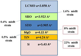
Each layer in this heterostructure was grown epitaxially. As depicted in the schematic diagram shown in Fig. 1, this work is facilitated by the deposition of epitaxial TiN (a = 4.24 Å), MgO (a = 4.22 Å), and STO (a = 3.905 Å) buffer layers. TiN was chosen because it grows epitaxially on Si (100) and has superior diffusion barrier properties. Three lattice planes of Si (a = 5.43 Å) match very well with four of TiN (a = 4.24 Å) and the epitaxial growth occurs via DME,[ Reference Narayan 12 , Reference Narayan and Larson 13 ] which can handle lattice strain in the range of 0–30%. TiN has an excellent lattice match with MgO, which has a misfit of about 8% with STO. Lattice constant of STO (3.905 Å)[ Reference Schmidbauer, Kwasniewski and Schwarzkopf 14 ] matches closely with that of LCMO (3.858 Å)[ Reference Lu, Wang, Kwon and Jia 15 ] and SRO (3.923 Å)[ Reference Koster, Klein, Siemons, Rijnders, Dodge, Eom, Blank and Beasley 16 ]. MgO and STO layers are used as intermediate layers between SRO and TiN in order to control oxidation and lattice mismatch between the top and bottom layers.
Schematic diagram showing the various layers and their expected lattice strains on the lattice-mismatched Si substrate.

As reported by previous researchers,[ Reference Baek and Eom 17 , Reference Giencke, Folkman, Baek and Eom 18 ] when STO was grown on a Si substrate by MBE, STO unit cell is rotated by 45° along the 〈001〉−axis (surface normal) with the Si substrate, which leads to matching of {220} planes of the film with {200} planes of Si resulting in a lattice mismatch of 1.7% (at room temperature), leading to the formation of dislocations, which form after only a few unit cells, leading to unrelaxed residual strain. When STO layer was grown on MgO/TiN-buffered Si substrate using DME paradigm, STO layer was grown strain-free (c film = 3.907 Å and c bulk = 3.905 Å) with cube-on-cube fashion, without any rotation, unlike in the previous case. In the case of TiN/Si (100) epitaxy with 22% misfit, 4/3 and 5/4 domains of TiN and Si alternate with equal frequency to account all the misfit where four lattice planes of TiN match with three of Si (100). An important feature of DME concept[ Reference Narayan 12 , Reference Narayan and Larson 13 ] is that most of the strain is relieved almost immediately upon initiation of growth, that is, within the first couple of monolayers of growth. In this way, lattice misfit strain accommodation is confined to the interface making it possible for the rest of the film to be grown free of defects and lattice strain. Inspite of ~22% lattice mismatch between TiN and Si (100), the epitaxial growth of TiN on Si (100) using DME paradigm was the key to subsequently grow epitaxial over-layers such as MgO, STO, SRO, and LCMO. The growth of over-layers occurred due to lattice-matching epitaxy. In addition to buffer layer, MgO can act as a strong diffusion barrier. Thus, this selection of buffer layers made it possible to integrate epitaxial thin films of LCMO/SRO heterostructures on Si (100).
Figure 2(a) presents a θ–2θ XRD pattern of the five-layer heterostructure. No evidence of additional phases or interfacial reaction products was observed in the XRD pattern. It is evident from this pattern that all the layers show preferential (00l) orientation, suggesting the epitaxial growth of the multilayered structure. From the 2θ XRD data for the (002) peak, we determined the OOP lattice parameter of LCMO to be 3.847 Å, close to the bulk value[ Reference Ramirez 4 , Reference Salamon and Jaime 5 , Reference Lu, Wang, Kwon and Jia 15 ] of 3.858 Å. As compared in Fig. 2(b), the φ-scan pattern of (111) reflection for LCMO was collected. This pattern shows four peaks separated by ~90° indicating its pseudocubic/rhombohedral symmetry and establishes the cube-on-cube relationship of the LCMO with the underlying substrate Si (100). The rocking curve of the LCMO (002) peak as the full-width at half-maximum of about 0.9°–1.1°.
(a) Typical θ–2θ (out of plane) XRD pattern of LCMO/SRO/STO/MgO/TiN/Si (100) showing (in log-scale) high quality, single phase and (00l) films of LCMO. (b) φ-scan patterns of LCMO (111) reflection collected at 2θ = 38.89°, ω = 19.94°, and χ = 56.25° for LCMO. This pattern shows four peaks separated by ~90° indicating its pseudocubic/rhombohedral symmetry, and establishing the cube-on-cube relationship with the underlying substrate Si (100).
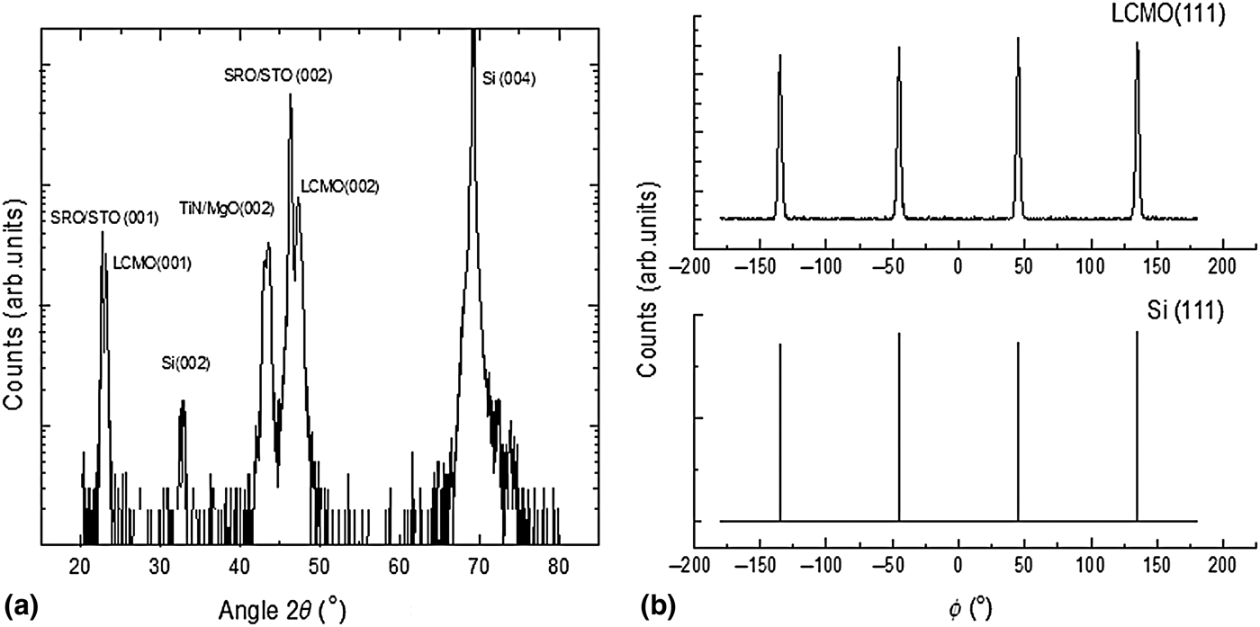
Figure 3(a) is a typical bright-field cross-section TEM image, in which the LCMO/SRO/STO/MgO/TiN/Si (100) layers are labeled. The top Pt layer was sputtered during the FIB-sample preparation process to protect the thin films underneath. The interfaces between different layers are sharp, without traces of diffusion, and secondary phases over a large area. All five layers are uniform and continuous. The film growth follows a layer-by-layer growth mode (Frank–van der Merwe or F–M mode). The thicknesses of LCMO, SRO, and STO are estimated to be ~100, ~200, and ~450 nm, respectively. To investigate the atomic structures at the interface regions between LCMO, SRO, and STO, high resolution transmission electron microscopy (HRTEM) images were collected, as shown in Figs. 3(b) and 3(c). The viewing direction is [110] zone of each phase. The three phases share the cubic structure and similar lattice constants. Therefore, one lattice of LCMO sits on one SRO lattice, which sits on another lattice of STO. The (010) plane of each phase connects with each other, showing a perfect cube-on-cube relationship. To further confirm the orientation relationships among different layers, the 〈110〉 zone axis electron diffraction patterns of LCMO/SRO/STO and STO/MgO/TiN/Si are obtained and shown in Figs 3(d) and 3(e), respectively. Since the lattice constants of STO, SRO, and LCMO are very close to each other (a STO = 3.905, a SRO = 3.923, and a LCMO = 3.858 Å), their diffraction points for low-index planes overlap with each other and therefore cannot be distinguished. However, the splitting of diffraction points for higher-index planes can be observed. The alignment of three sets of diffraction spots confirming the cube-on-cube epitaxial relationships among the layers on the Si substrate.
(a) Bright-field cross-section TEM image taken from LCMO/SRO/STO/MgO/TiN/Si (100), with all layers marked. The top layer of Pt was sputtered during FIB sample preparation process. The scale bar is 200 nm. (b) HRTEM image of SRO/LCMO interface. (c) HRTEM image of SRO/STO interface. (d) 〈110〉 zone-axis pattern (ZAP) for the STO/SRO/LCMO system. (e) 〈110〉 zone-axis pattern (ZAP) for the STO/MgO/TiN/Si system.

Now we discuss the magnetic properties. The in-plane temperature (4–400 K) (M-T) and magnetic-field-dependent magnetization (M–H) measurements have been performed on three of the heterostructures, namely, SRO/STO/MgO/TiN/Si (100), LCMO/STO/MgO/TiN/Si (100), and LCMO/SRO/STO/MgO/TiN/Si (100). Here the STO/MgO/TiN-buffered Si (100) substrate is shown to be diamagnetic and should not contribute to the overall magnetic response. Figure 4 presents the variation of magnetic moment as a function of temperature measured when all the three samples were cooled from 400 K under the magnetic field of 0.1 T. As it can be noted clearly, SRO/STO/MgO/TiN/Si (100) shows paramagnetic to ferromagnetic transition at the Curie temperature (T C) of 168 K followed by a clear saturation in magnetization down to 4 K (see curve in blue), consistent with the previous works reported for lattice-matched STO substrates.[ Reference Schmidbauer, Kwasniewski and Schwarzkopf 14 , Reference Ke, Rzchowski, Belenky and Eom 7 – Reference Singamaneni, Prater and Narayan 11 ] The spin magnetic moment of this sample is estimated at 1.2 µB per Ru4+ ion, consistent with previously reported values (1.1–1.6 µB per Ru4+ ion) for the bulk SRO thin films. As shown by the curve in red, the sample with only LCMO layer exhibits characteristic[ Reference Ramirez 4 , Reference Salamon and Jaime 5 ] T C at about 240 K. The saturation magnetization is estimated at 3.3 µB per Mn ion, a bit smaller than the expected spin moment (3.5 µB per Mn ion), possibly due to unavoidable oxygen vacancies. Similar Curie temperatures are obtained from the temperature-dependent magnetic moment curve (in black) collected from the LCMO/SRO/STO/MgO/TiN/Si (100) heterostructure.
Field cooling (FC) magnetic moment versus temperature (M–T) curves of LCMO/SRO/STO/MgO/TiN/Si (100) (in black), SRO/STO/MgO/TiN/Si (100) (in blue) and LCMO/STO/MgO/TiN/Si (100) (in red). The data were collected during the warming cycle under the measuring field of 0.1 T after each sample had been cooled under the field of 0.1 T. The magnetic field is applied along the 〈100〉 direction of the sample.

As shown in Fig. 5, the field cooled (FC, 0.1 T) isothermal (4 K) M–H measurements have been performed on all three samples. The M–H curve (in blue) recorded from SRO shows clear saturation behavior characterized by coercive field (H c) of 4051 Oe (see inset of Fig. 5), consistent with the literature reports[ Reference Gan, Rao, Eom, Garrett and Lee 6 , Reference Ke, Rzchowski, Belenky and Eom 7 – Reference Singamaneni, Prater and Narayan 11 ] on relaxed SRO thin films. The M–H curve (in red) recorded from LCMO layer also reveals a clear saturation behavior characterized by H c of 625 Oe (see inset of Fig. 5), a characteristic feature of soft ferromagnetic material, also consistent with the literature reports.[ Reference Ramirez 4 , Reference Salamon and Jaime 5 ] The M–H curve (in black) recorded from the LCMO/SRO heterostructure exhibits two distinct magnetic switchings: one due to the reversal of the LCMO, corresponding to the low and sharp switching field of 860 Oe; and the second one is associated with the SRO layer that corresponds to the high and broad switching field of 7600 Oe. The Hc of the LCMO/SRO layer is 850 Oe (see inset of Fig. 5). The study of interface magnetic coupling in bilayers involving manganites with other layers has been widely reported in the past.[ Reference Singamaneni, Prater and Narayan 19 – Reference Chopdekar, Arenholz and Suzuk 33 ] Similar enhancement in switching field (7309 Oe) was observed[ Reference Singamaneni, Prater and Narayan 19 ] when the SRO layer is interfaced with the ferroelectric and antiferromagnetic BiFeO3 layers. It should be noted that these switching field values are much higher than the values observed for individual layers. Also, the pinned SRO layer at the interface might play an important role in the coercivity (20 kOe) enhancement as recently observed[ Reference Ning, Wang and Zhang 20 ] in the SRO–NiO system. We believe that the super exchange interaction between Ru and Mn ions at LCMO/SRO interface might lead to enhanced coercive fields of these layers. The detailed study on the magnetic nature of LCMO/SRO interface is underway.
Isothermal (4 K) in-plane M–H data collected on LCMO/SRO/STO/MgO/TiN/Si (100) (in black), SRO/STO/MgO/TiN/Si (100) (in blue), and LCMO/STO/MgO/TiN/Si (100) (in red). The inset shows the zoomed version of the main panel to highlight the coercive fields (H c) of all three samples.

Conclusions
In conclusion, we have grown strain-free LCMO/SRO heterostructures on (100)-oriented Si using PLD through DME paradigm. In order to prevent interfacial interactions with oxygen and to achieve epitaxial growth of LCMO/SRO films, MgO and STO films were used as intermediate layers between LCMO/SRO and TiN layers. SQUID magnetization measurements have successfully reproduced the pristine ferromagnetic properties of LCMO and SRO layers deposited on lattice-mismatched Si substrates, with characteristic Curie temperatures of 240 and 168 K, respectively. When conjoined, the resultant heterostructures LCMO/SRO showed enhanced switching field of SRO layer. As LCMO and SRO layers are quite thick (100–200 nm) in this study, we believe that such changes in the magnetic properties could derive from the bulk parts of the individual layers. There might be a minimal contribution emanating from the super exchange interaction between Ru and Mn ions at the interface; this certainly needs additional study to resolve the two components. We conclude that LCMO/SRO heterostructures grown on Si show potential for the scalable integration of ferromagnetic functionality with Si based microelectronics and nanoelectronics.
Acknowledgments
S.S.R. acknowledges National Academy of Science (NAS), USA for awarding the NRC postdoctoral research associate fellowship. The authors are pleased to acknowledge the support of the Army Research Office under Grant W911NF-04-D-0003. Also, the authors acknowledge the use of the Analytical Instrumentation Facility (AIF) at North Carolina State University, which is supported by the State of North Carolina and the National Science Foundation.


